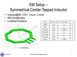
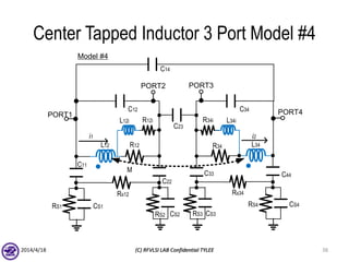
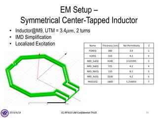
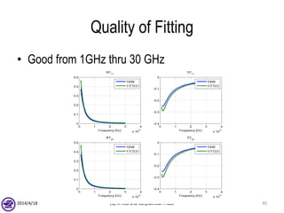
Downloaded 57 times


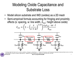
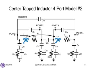
![Design Flow of Modeling Fitting
2014/4/18 Tao-Yi Lee @ RFVLSILAB 3
Start
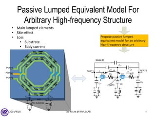
Propose passive lumped
equivalent model for an arbitrary
high-frequency structure
Solve Y parameter matrix [Y] of the
lumped equivalent network
Rum EM simulations of the desired
structures, obtain [YEM]
Program the Ycost(R1, L1, C1)=[Y]-
[YEM] matrix into MATLAB script as
cost functions in numerical
analysis
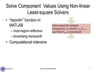
Solve values for lumped
component, i.e. find R1, L1, C1,…,
such that Ycost is minimized
Stop](https://image.slidesharecdn.com/rfmodelfitting-140418091827-phpapp02/85/Generiic-RF-passive-device-modeling-3-320.jpg)
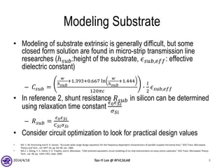
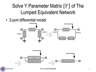
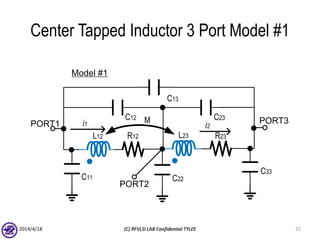
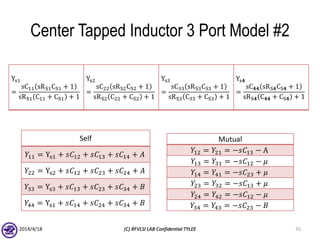
![Solve Y Parameter Matrix 𝑌 of The
Lumped Equivalent Network
• Definition of Y parameters
– Yij =
Ii
Vj Vk=0 for k≠j
–
𝐼1
𝐼2
𝐼3
𝑌11 𝑌12 𝑌13
𝑌21 𝑌22 𝑌23
𝑌31 𝑌32 𝑌33
𝑉1
𝑉2
𝑉3
– Short all other terminals to ground reference and write down
𝑌𝑖𝑗 as function of lumped elements
– Simple; Can be done by inspection
– Matrix symmetry of passive networks
2014/4/18 Tao-Yi Lee @ RFVLSILAB 9
Solve Y parameter matrix [Y] of the
lumped equivalent network](https://image.slidesharecdn.com/rfmodelfitting-140418091827-phpapp02/85/Generiic-RF-passive-device-modeling-9-320.jpg)
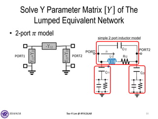
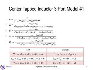
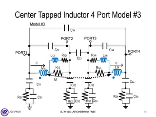
![Run EM Simulations Of The Desired
Structures, Obtain 𝑌𝐸𝑀
• Convert S-parameters to
Y-parameters via post-
processing
2014/4/18 Tao-Yi Lee @ RFVLSILAB 13
Rum EM simulations of the desired
structures, obtain [YEM]
YEMSEM](https://image.slidesharecdn.com/rfmodelfitting-140418091827-phpapp02/85/Generiic-RF-passive-device-modeling-13-320.jpg)
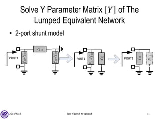
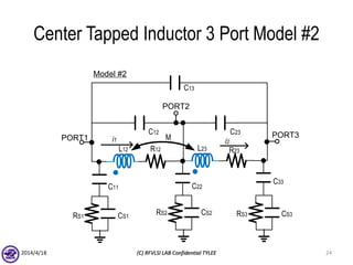
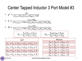
![Define The Minimization Problem In
MATLAB
∀i, j, minimize
R1,R2,…,L1,L2,…,C1,C2,…
ΔYij
= minimize
R1,R2,…,L1,L2,…,C1,C2,…
𝐘 − 𝐘𝐄𝐌
subject to all passive elements ≥ 0
2014/4/18 Tao-Yi Lee @ RFVLSILAB 14
Program the Ycost(R1, L1, C1)=[Y]-
[YEM] matrix into MATLAB script as
cost functions in numerical
analysis](https://image.slidesharecdn.com/rfmodelfitting-140418091827-phpapp02/85/Generiic-RF-passive-device-modeling-14-320.jpg)

The document describes the process of modeling passive RF devices using lumped element equivalent circuits. It outlines the generic modeling flow, which involves proposing a lumped element model, solving the Y parameter matrix, running EM simulations to obtain YEM, defining a cost function in MATLAB, and solving for component values to minimize the cost function. Examples are provided for modeling inductors, center tapped inductors, transmission lines, and transformers using this process.


![RF Circuit Design - [Ch2-2] Smith Chart](https://cdn.slidesharecdn.com/ss_thumbnails/ch2-2-150613064401-lva1-app6891-thumbnail.jpg?width=640&height=640&fit=bounds)


![RF Circuit Design - [Ch2-1] Resonator and Impedance Matching](https://cdn.slidesharecdn.com/ss_thumbnails/ch2-1-150613064353-lva1-app6892-thumbnail.jpg?width=640&height=640&fit=bounds)


