This document provides summaries of reviews for the book "Digital Design: An Embedded Systems Approach Using Verilog" by Peter Ashenden. The reviewers praise the book for teaching digital design using an embedded systems approach and modern design methodology. They note it provides excellent coverage of all aspects of embedded system design, from logic design to processors, memory, I/O and implementation technologies. The book is also described as intuitive, accessible, instructive and a pleasure to read.


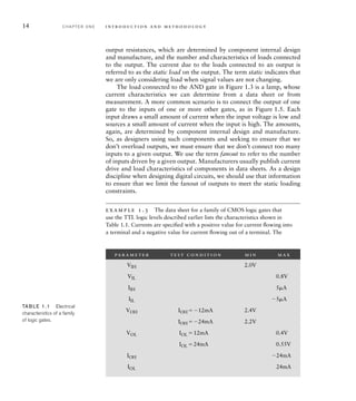

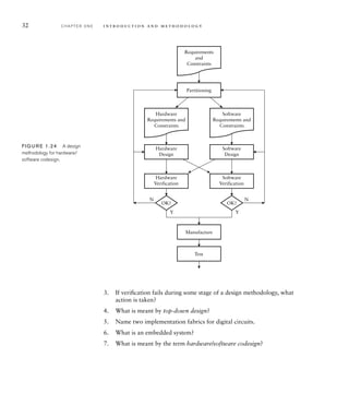


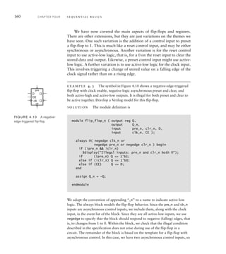
![56 C H A P T E R T W O c o m b i n a t i o n a l b a s i c s
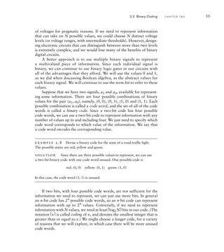
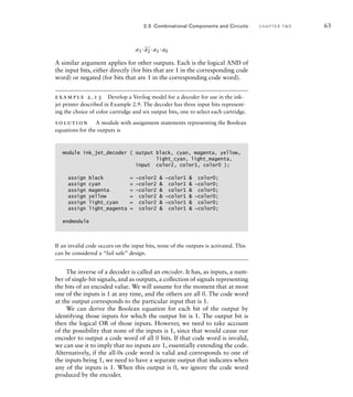
example 2.9 Many ink-jet printers have six cartridges for different
colored ink: black, cyan, magenta, yellow, light cyan and light magenta. A multi-
bit signal in such a printer indicates selection of one of the colors. Devise a
minimal length code for the signal.
solution Since there are six values to encode, the minimal length code
is ⎡log26⎤3 bits long. There are 23
8 possible code words, so two will remain
unused. One possible code is
black: (0, 0, 1) cyan: (0, 1, 0) magenta: (0, 1, 1)
yellow: (1, 0, 0) light cyan: (1, 0, 1) light magenta: (1, 1, 0)
While it might make sense in some cases to use the shortest code, in
other cases a longer code is better. A particular case of a non–minimal-
length code is a one-hot code, in which the code length is the number
of values to be encoded. Each code word has exactly one 1 bit with the
remaining bits 0. The advantage of a one-hot code becomes clear when
we want to test whether the encoded multibit signal represents a given
value; we just test the single-bit signal corresponding to the 1 bit in the
code word for that value.
example 2.10 Devise a one-hot code for the state of the traffic light
described in a preceding example.
solution Since there are three values to encode, we need a 3-bit one-hot
code. A possible code is
red: (1, 0, 0) yellow: (0, 1, 0) green: (0, 0, 1)
With this code, the left-most bit can be used to activate the red light, the middle
bit to activate the yellow light, and the right-most bit to activate the green light.
No additional circuitry is needed to decode the encoded signals to determine
which light to activate.
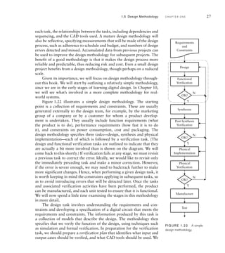
2.2.1 U S I N G V E C TO R S F O R B I N A R Y C O D E S
Since a collection of binary coded bits conceptually represents a single
piece of information, it would be convenient to be able to represent it as
a single net in Verilog. We can do so using a vector net instead of using
several individual nets. For example, if we need a net w to carry a 5-bit
binary coded value, we could declare it as
wire [4:0] w;](https://image.slidesharecdn.com/digitaldesign-anembeddedsystemsapproachusingverilog-220525003453-7ebc98ea/85/Digital-Design-An-Embedded-Systems-Approach-Using-Verilog-pdf-77-320.jpg)
![This defines w to be a collection of five nets, w[4], w[3], w[2], w[1] and
w[0], each of which is a single bit. Apart from condensing the declaration
of the nets quite considerably, using vectors for encoded values gives us
many other benefits, as we shall see throughout this book.
When we declare a vector net or port, the part in brackets (4:0 in the
above example) specifies the index range for the elements of the vector.
The first value is the index of the left-most element, and the second value
is the index of the right-most element. If we want to number elements in
descending order, we make the left-most index greater than the right-most
index, as in the above example. We can also number elements in ascend-
ing order by making the left-most index less than the right-most index, as
in the following:
wire [1:3] a;
Here, the elements from left to right are w[1], w[2] and w[3]. The choice
between ascending and descending order is often a question of style, and
may be addressed by coding guidelines used in an organization. This
example also shows that we don’t have to use 0 for the least index value;
it can be any number.
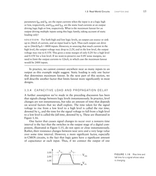
example 2.11 Assume that the one-hot code for the traffic lights in
Example 2.10 is represented using a 3-element vector with element 1
corresponding to red, 2 to yellow and 3 to green. Develop a Verilog model for a
light controller that has an encoded input, an encoded output, and a single-bit
input that enables the lights. When the enable input is 1, the encoded output is
the same as the encoded input. When the enable input is 0, all bits of the output
are 0.
solution One approach is to control each bit of the output by “AND-
ing” the corresponding input with the enable bit. A module that does this is
module light_controller_and_enable
( output [1:3] lights_out,
input [1:3] lights_in,
input enable );
assign lights_out[1] = lights_in[1] enable;
assign lights_out[2] = lights_in[2] enable;
assign lights_out[3] = lights_in[3] enable;
endmodule
2.2 Binary Coding C H A P T E R T W O 57](https://image.slidesharecdn.com/digitaldesign-anembeddedsystemsapproachusingverilog-220525003453-7ebc98ea/85/Digital-Design-An-Embedded-Systems-Approach-Using-Verilog-pdf-78-320.jpg)
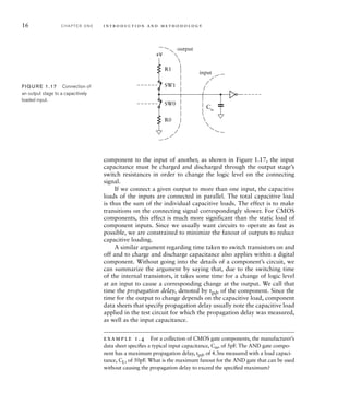
![58 C H A P T E R T W O c o m b i n a t i o n a l b a s i c s
An alternative approach is to use the enable input to select whether to assign the
input to the output (when enable is 1) or to set the output to all 0 bits otherwise.
A module that takes this approach is
module light_controller_conditional_enable
( output [1:3] lights_out,
input [1:3] lights_in,
input enable );
assign lights_out = enable ? lights_in : 3'b000;
endmodule
The assignment statement in this module uses the ? : operator to select between
the alternatives. Note that we use the notation 3'b000 to form a literal vector
value of three 0 bits. The notation 'b specifies that a binary code word follows,
and the number before 'b specifies how many bits in the vector.
2.2.2 B I T E R R O R S
While digital circuits are much more immune to noise than analog electrical
circuits, they are not completely immune from interference. The effect of
interference is occasionally to change the value of a signal from 0 to 1 or
from 1 to 0. We sometimes prosaically call this a bit flip. If the signal is a
single bit representing a logical condition, the rest of the circuit continues
operating on the incorrect value, possibly causing erroneous outputs. If
the signal is one of several bits in a binary-coded representation of some
information, there are two possibilities. The flipped bit results in the code
word being changed either to another valid code word or to a bit com-
bination that is not a valid code word. If the result is a valid code word,
the rest of the circuit operates on the incorrect value, as in the single-bit
case, possibly producing erroneous outputs. If the result is an invalid code
word, operation of the circuit depends on how we deal with invalid codes
in the design.
One design approach is to consider invalid code words as “impossible”
inputs, and not to specify the behavior of circuits that operate on invalid
inputs. If we adopt this approach, the actual behavior of the circuits will
depend on the implementation for the valid-code-word cases and on opti-
mizations performed by CAD tools. It may be acceptable not to care about
the circuit output values for invalid code words, particularly if cost reduc-
tion is a driving constraint. For example, in a mass-produced consumer
toy, no one really cares about a once-a-year glitch, particularly if fixing it
would increase the cost from $1.00 to $1.05.](https://image.slidesharecdn.com/digitaldesign-anembeddedsystemsapproachusingverilog-220525003453-7ebc98ea/85/Digital-Design-An-Embedded-Systems-Approach-Using-Verilog-pdf-79-320.jpg)
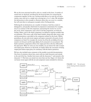
![64 C H A P T E R T W O c o m b i n a t i o n a l b a s i c s
example 2.14 Design an encoder for use in a domestic burglar alarm that
has sensors for each of eight zones. Each sensor signal is 1 when an intrusion
is detected in that zone, and 0 otherwise. The encoder has three bits of output,
encoding the zone as follows:
Zone 1: 000 Zone 2: 001 Zone 3: 010 Zone 4: 011
Zone 5: 100 Zone 6: 101 Zone 7: 110 Zone 8: 111
solution Since all code words are used, we need a separate output to
indicate when there is a valid code-word output. The module definition is
module alarm_eqn ( output [2:0] intruder_zone,
output valid,
input [1:8] zone );
assign intruder_zone[2] = zone[5] | zone[6] |
zone[7] | zone[8];
assign intruder_zone[1] = zone[3] | zone[4] |
zone[7] | zone[8];
assign intruder_zone[0] = zone[2] | zone[4] |
zone[6] | zone[8];
assign valid = zone[1] | zone[2] | zone[3] | zone[4] |
zone[5] | zone[6] | zone[7] | zone[8];
endmodule
The left-most bit of the output code is 1 when any of the zone 5 through zone
8 inputs is 1, so the equation for that output is the logical OR of those zone
inputs. The equations for the other two output code bits are derived similarly.
The valid output is the logical OR of all of the zone inputs.
Now let’s consider the possibility of more than one input to an encoder
being 1 at a time. The design we described above would produce an incor-
rect output, possibly an invalid code word. The solution is to assign pri-
orities to the inputs, so that if multiple inputs are 1, the encoder outputs
the code word corresponding to the input with highest priority. Such an
encoder is called, not surprisingly, a priority encoder. One application
of priority encoders is to prioritize interrupts in embedded systems. (We
describe interrupts in Chapter 8.)
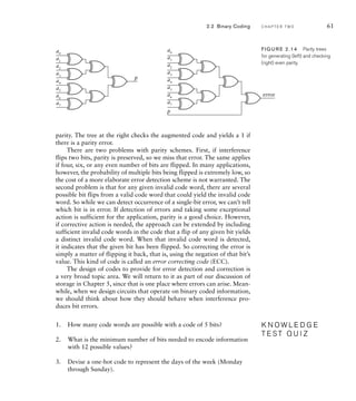
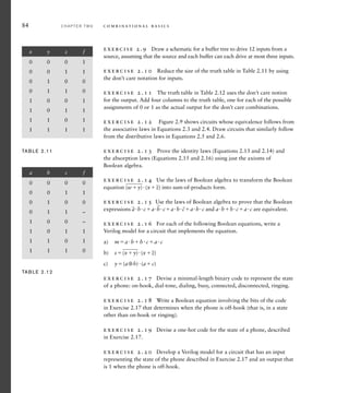
example 2.15 Revise the encoder for the burglar alarm to be a priority
encoder, with zone 1 having highest priority, down to zone 8 having lowest priority.
solution The port list is unchanged, since we need the same inputs and
outputs for the encoder. The truth table for the priority encoder is shown in](https://image.slidesharecdn.com/digitaldesign-anembeddedsystemsapproachusingverilog-220525003453-7ebc98ea/85/Digital-Design-An-Embedded-Systems-Approach-Using-Verilog-pdf-85-320.jpg)
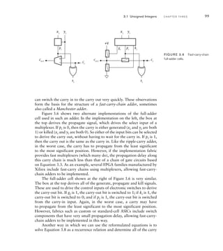
![Table 2.9. From this, we can derive the Boolean equations for each bit of the
output. A revised module definition is shown below.
module alarm_priority ( output [2:0] intruder_zone,
output valid,
input [1:8] zone );
wire [1:8] winner;
assign winner[1] = zone[1];
assign winner[2] = zone[2] ~zone[1];
assign winner[3] = zone[3] ~(zone[2] | zone[1]);
assign winner[4] = zone[4] ~(zone[3] | zone[2] | zone[1]);
assign winner[5] = zone[5] ~(zone[4] | zone[3] | zone[2] |
zone[1]);
assign winner[6] = zone[6] ~(zone[5] | zone[4] | zone[3] |
zone[2] | zone[1]);
assign winner[7] = zone[7] ~(zone[6] | zone[5] | zone[4] |
zone[3] | zone[2] | zone[1]);
assign winner[8] = zone[8] ~(zone[7] | zone[6] | zone[5] |
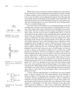
zone[4] | zone[3] | zone[2] |
zone[1]);
assign intruder_zone[2] = winner[5] | winner[6] |
winner[7] | winner[8];
assign intruder_zone[1] = winner[3] | winner[4] |
winner[7] | winner[8];
assign intruder_zone[0] = winner[2] | winner[4] |
winner[6] | winner[8];
assign valid = zone[1] | zone[2] | zone[3] | zone[4] |
zone[5] | zone[6] | zone[7] | zone[8];
endmodule
2.3 Combinational Components and Circuits C H A P T E R T W O 65
zone i n t r u d e r _ z o n e
(1) (2 ) (3) (4) (5) (6) (7) ( 8 ) ( 2 ) ( 1 ) ( 0 ) v a l i d
1 – – – – – – – 0 0 0 1
0 1 – – – – – – 0 0 1 1
0 0 1 – – – – – 0 1 0 1
0 0 0 1 – – – – 0 1 1 1
0 0 0 0 1 – – – 1 0 0 1
0 0 0 0 0 1 – – 1 0 1 1
0 0 0 0 0 0 1 – 1 1 0 1
0 0 0 0 0 0 0 1 1 1 1 1
0 0 0 0 0 0 0 0 – – – 0
TAB LE 2.9 Truth table for a
priority encoder for a burglar alarm.](https://image.slidesharecdn.com/digitaldesign-anembeddedsystemsapproachusingverilog-220525003453-7ebc98ea/85/Digital-Design-An-Embedded-Systems-Approach-Using-Verilog-pdf-86-320.jpg)
![66 C H A P T E R T W O c o m b i n a t i o n a l b a s i c s
In this module, each element of the internal net winner indicates when the cor-
responding zone is 1 and has not lost to a higher priority zone. The encoder
then uses the elements of the internal net instead of the zone inputs directly to
generate the output code word. Another way of expressing this in Verilog is
shown in the following module:
module alarm_priority_1 ( output [2:0] intruder_zone,
output valid,
input [1:8] zone );
assign intruder_zone = zone[1] ? 3'b000 :
zone[2] ? 3'b001 :
zone[3] ? 3'b010 :
zone[4] ? 3'b011 :
zone[5] ? 3'b100 :
zone[6] ? 3'b101 :
zone[7] ? 3'b110 :
zone[8] ? 3'b111 :
3'b000;
assign valid = zone[1] | zone[2] | zone[3] | zone[4] |
zone[5] | zone[6] | zone[7] | zone[8];
endmodule
The conditional assignment in this module tests a series of conditions to
determine the value to assign to the net intruder_zone. First the zone 1 input is
tested, and the result assigned 000 if the zone 1 input is 1. Otherwise, the zone
2 input is tested, and the result assigned 001 if the zone 2 input is 1. Testing con-
tinues in this way, with priority implied by the order of testing the conditions.
This form of assignment for priority encoding is much easier to understand, and
leaves the hard work of determining and optimizing the Boolean equations to
the synthesis CAD tool.
BCD Code and 7-Segment Decoders
One form of information that we might wish to encode is numeric infor-
mation. As we mentioned earlier, we will look at this topic in detail in
Chapter 3. However, in this section, we will look at a particular form of
numeric coding called binary coded decimal (BCD). If we consider just a
single decimal digit, the ten possible values are 0, 1, 2, 3, 4, 5, 6, 7, 8 and
9. We need at least 4 bits in a binary code for these values. There are a
large number of possible codes, but BCD is the most common, having the
following code words:
0: 0000 1: 0001 2: 0010 3: 0011 4: 0100
5: 0101 6: 0110 7: 0111 8: 1000 9: 1001](https://image.slidesharecdn.com/digitaldesign-anembeddedsystemsapproachusingverilog-220525003453-7ebc98ea/85/Digital-Design-An-Embedded-Systems-Approach-Using-Verilog-pdf-87-320.jpg)
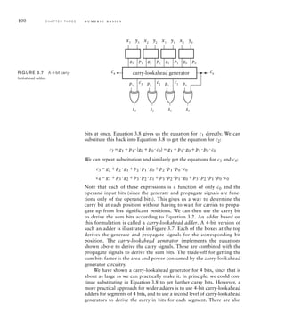
![If we have more than one decimal digit of information to represent, we
simplyusegroupsoffourbits,witheachgroupcorrespondingtoonedecimal
digit. For example, a system that deals with three-digit numbers would use
a 12-bit code. The number 493 would be encoded as 0100 1001 0011.
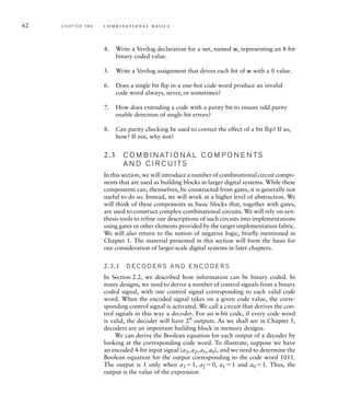
Many digital systems display decimal numbers using 7-segment dis-
plays. Each display digit consists of seven separate lights, arranged as
shown in Figure 2.15. If we have a digit encoded using BCD and we need
to display the digit on a 7-segment display, we need a 7-segment decoder.
Strictly speaking, we should call it a “7-segment code converter,” since it
converts from a BCD code input to a 7-segment code output. However,
the term “7-segment decoder” is widely used. Assuming a segment is lit if
its input is 1, we need a 7-bit code for representing the digits 0 through 9.
The code word for each digit has a 1 bit corresponding to each seg-
ment that is lit and a 0 bit corresponding to each segment that is not lit.
A 7-segment decoder then converts between BCD and this 7-bit code. One
possible code is shown in Figure 2.16, with the bits corresponding left to
right with segments g through a.
2.3 Combinational Components and Circuits C H A P T E R T W O 67
a
b
c
d
e
f g
FIG U R E 2.15 A 7-segment
display digit. The segments are
named “a” through “g,” as shown.
0111111 0000110 1011011 1001111 1100110
1101101 1111101 0000111 1111111 1101111
FIG U R E 2.16 A 7-segment
code for decimal digits. In each
code word, the bits correspond to
segments g through a in left-to-
right order.
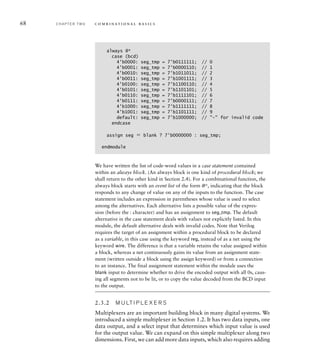
example 2.16 Develop a Verilog model for a 7-segment decoder. Include
an additional input, blank, that overrides the BCD input and causes all segments
not to be lit.
solution We could determine the BCD code words that result in each
segment being lit, and so derive Boolean equations for each segment output.
However, that would make the model hard to understand. A better approach is
to list the 7-bit code word corresponding to each BCD code word, as we did in
Figure 2.16. A module that does this is
module seven_seg_decoder ( output [7:1] seg,
input [3:0] bcd,
input blank );
reg [7:1] seg_tmp;
(continued)](https://image.slidesharecdn.com/digitaldesign-anembeddedsystemsapproachusingverilog-220525003453-7ebc98ea/85/Digital-Design-An-Embedded-Systems-Approach-Using-Verilog-pdf-88-320.jpg)
![further select inputs to encode the choice of input to drive the output.
Second, we can use multiplexers in parallel to select between two sources
of multibit encoded data. Let’s look at the alternatives in more detail.
Suppose that, instead of selecting between two input bits, we need to
select between four input bits. Since there are four input sources, we need
to have four values for the select input. We can encode the select input
using two bits. Figure 2.17 shows a 4-to-1 multiplexer. The select input is
drawn as a thicker line to indicate that it is a multibit encoded input. In
this book, we will mostly use line thickness to distinguish between single-
bit and multibit signals. Occasionally, where we want to emphasis that a
signal is multibit, we will add a stroke across the line and show the num-
ber of bits, as in Figure 2.17. The code for the select input is
00: input 0 01: input1 10: input 2 11: input 3
We could describe a gate circuit to implement the multiplexer, but
there is little point, for two reasons. First, a synthesis tool would probably
optimize the circuit, changing it from what we specify. Second, in a num-
ber of implementation fabrics, multiplexers can be constructed from indi-
vidual transistors more efficiently than as a circuit of gates. Multiplexers
would be considered primitive elements in those fabrics. So instead of
a gate-level circuit, we will just consider how to express a multiplexer
function in Verilog.
example 2.17 Develop a Verilog model for a 4-to-1 multiplexer.
solution The module definition is
module multiplexer_4_to_1 ( output reg z,
input [3:0] a,
input sel );
always @*
case (sel)
2'b00: z a[0];
2'b01: z a[1];
2'b10: z a[2];
2'b11: z a[3];
endcase
endmodule
The case statement in the always block uses the value of the sel input to deter-
mine which input bit to copy to the output. This example illustrates a further
point about using always blocks to model combinational functions. As we
2.3 Combinational Components and Circuits C H A P T E R T W O 69
0
1
2
3
2
FIG U R E 2.17 A 4-to-1
multiplexer.](https://image.slidesharecdn.com/digitaldesign-anembeddedsystemsapproachusingverilog-220525003453-7ebc98ea/85/Digital-Design-An-Embedded-Systems-Approach-Using-Verilog-pdf-90-320.jpg)
![70 C H A P T E R T W O c o m b i n a t i o n a l b a s i c s
mentioned in Example 2.16, the target of the assignments in the block must be
declared as a variable, using the keyword reg in this case. When the target is a
port of the module, the reg declaration can be combined with the output port
declaration.
We can further expand this multiplexer to have eight data inputs,
which would require a 3-bit select input. The number of data inputs need
not be a power of 2. If it is not, then the select input code will have unused
code words. We must then ensure that an invalid code word is never pre-
sented to the select input. In general, a multiplexer having N input bits
needs ⎡log2N⎤ bits for the select input, since the select input carries a
binary code requiring N values.
Now let’s consider using multiplexers to select between two sources
of encoded data. If the code length is m (that is, each code word has
m bits), we can use m two-input multiplexers, one for each bit of the two
data sources. This is illustrated in Figure 2.18 for selecting between two
sources each of three bits. The circuit at the top of the figure shows the
three separate 2-to-1 multiplexers. At the bottom of the figure is a symbol
that represents a 2-to-1 multiplexer operating on the 3-bit encoded data
inputs and output.
example 2.18 Develop a Verilog model for the 3-bit 2-to-1 multiplexer.
solution The module definition is
module multiplexer_3bit_2_to_1 ( output [2:0] z,
input [2:0] a0, a1,
input sel );
assign z = sel ? a1 : a0;
endmodule
We can, of course, combine these two forms of expansion. If we need
to select between N sources of data, each of which is encoded with m bits,
we simply use m lots of N-to-1 multiplexers. The details are left as an
exercise.
Before we leave the topic of multiplexers, it is interesting to note that
all Boolean functions can be expressed in terms of multiplexers combined
with negation. To illustrate, consider the function that we examined ear-
lier, f(xy)
_
z whose truth table is shown in Table 2.2. This function
can be implemented using the circuit shown in Figure 2.19. Note the use
of a literal 0 value for one input. This can be implemented by hard wiring
0
1
0
1
0
1
0
1
a0(0)
a1(0)
z(0)
a0 3
3
3
a1
z
a0(1)
a1(1)
z(1)
a0(2)
a1(2)
sel
sel
z(2)
FIG U R E 2.18 A circuit for
a 2-to-1 multiplexer for 3-bit data
sources (top), and a symbol for the
multiplexer (bottom).
f
z
y
x
0 0
1 0
1
FIG U R E 2.19 Implementing
a Boolean function using
multiplexers.](https://image.slidesharecdn.com/digitaldesign-anembeddedsystemsapproachusingverilog-220525003453-7ebc98ea/85/Digital-Design-An-Embedded-Systems-Approach-Using-Verilog-pdf-91-320.jpg)
![Boolean equations, the design will probably implement those equations
directly, so expressing the correctness conditions as Boolean equations
gains nothing. A better approach is to determine some more abstract con-
ditions that are required to hold, and to test that the design satisfies those
conditions.
example 2.21 Develop a testbench model for the light_controller_and_enable
module for the traffic light control circuit of Example 2.11. Verify the conditions
that, when the enable input is 1, the output is the same as the light input, and
when the enable input is 0, all light outputs are inactive.
solution The testbench model includes an instance of the design under
verification, as well as code to apply test cases and to check for correct outputs.
The organization of these components is shown in Figure 2.23.
DUV
light_controller
apply_test_cases
lights_in
enable
lights_out
check_outputs
FIG U R E 2.23 Organization
of the testbench for the light
controller.
2.4 Verification of Combinational Circuits C H A P T E R T W O 75
Since the testbench is a Verilog model, it needs a modue definition. However,
since there are no external connections to the testbench, the module has no
ports. The module definition is
`timescale 1ms/1ms
module light_testbench;
wire [1:3] lights_out;
reg [1:3] lights_in;
reg enable;
light_controller_and_enable duv ( .lights_out(lights_out),
.lights_in(lights_in),
.enable(enable) );
initial begin
enable = 0; lights_in = 3'b000;
#1000 enable = 0; lights_in = 3'b001;
#1000 enable = 0; lights_in = 3'b010;
(continued)](https://image.slidesharecdn.com/digitaldesign-anembeddedsystemsapproachusingverilog-220525003453-7ebc98ea/85/Digital-Design-An-Embedded-Systems-Approach-Using-Verilog-pdf-96-320.jpg)
![78 C H A P T E R T W O c o m b i n a t i o n a l b a s i c s
Another thing to note about the test cases in the example is that the
Verilog code is very repetitious. Each test case involves an assignment to
the two inputs, followed by waiting for an interval. In larger models, there
are more statements for each test case, and writing them repeatedly can be
error prone. Fortunately, Verilog provides a feature that lets us abstract out
the common parts of the test cases. We can write a task containing the com-
mon statements, and invoke the task once for each test case. We provide
the particular values to use in each test case as ports to the procedure.
example 2.22 Revise the testbench model of Example 2.21 to use a task
for applying the test cases.
solution The entity declaration is unchanged. The revised module
definition is
`timescale 1ms/1ms
module light_testbench1;
wire [1:3] lights_out;
reg [1:3] lights_in;
reg enable;
task apply_test ( input enable_test,
input [1:3] lights_in_test );
begin
enable = enable_test; lights_in = lights_in_test;
#1000;
end
endtask
light_controller_and_enable duv ( .lights_out(lights_out),
.lights_in(lights_in),
.enable(enable) );
initial begin
apply_test(0, 3'b000);
apply_test(0, 3'b001);
apply_test(0, 3'b010);
apply_test(0, 3'b100);
apply_test(1, 3'b001);
apply_test(1, 3'b010);
apply_test(1, 3'b100);
apply_test(1, 3'b000);
apply_test(1‚ 3'b111);
$finish;
end
(continued)](https://image.slidesharecdn.com/digitaldesign-anembeddedsystemsapproachusingverilog-220525003453-7ebc98ea/85/Digital-Design-An-Embedded-Systems-Approach-Using-Verilog-pdf-99-320.jpg)


![example 3.2 Suppose we are designing a scientific instrument to measure
the time interval between two random events very precisely, with a resolution of
nanoseconds (1ns109 seconds). Events may occur as much as a day apart.
How many bits are needed to represent the interval as a number of nanoseconds?
solution There are 109
nanoseconds per second, and 60602486,400
seconds per day, so the largest number we need to allow for is 8.641013
. The
number of bits needed is
⎡log2(8.641013
)⎤
⎡
log(8.641013)
log2 ⎤⎡46.296...⎤47
So at least 47 bits are needed.
Unsigned Integers in Verilog
We saw in Section 2.1.3 that we can use vectors to model binary coded
data. Since unsigned binary is just one form of binary code, we can use
vectors for numeric data also, specifying ranges of index values for nets,
variables and ports, and using indexing to refer to individual bits. When
we look at arithmetic operations on unsigned integers, we will see how
they can be modeled in Verilog as operations on vectors.
example 3.3 Develop a Verilog model of a 4-to-1 multiplexer that selects
among four unsigned 6-bit integers.
solution The module definition is
module multiplexer_6bit_4_to_1
( output reg [5:0] z,
input [5:0] a0, a1, a2, a3,
input [1:0] sel );
always @*
case (sel)
2'b00: z = a0;
2'b01: z = a1;
2'b10: z = a2;
2'b11: z = a3;
endcase
endmodule
3.1 Unsigned Integers C H A P T E R T H R E E 89](https://image.slidesharecdn.com/digitaldesign-anembeddedsystemsapproachusingverilog-220525003453-7ebc98ea/85/Digital-Design-An-Embedded-Systems-Approach-Using-Verilog-pdf-110-320.jpg)
![Recall that the largest value that can be represented with n bits is
2n
1. Suppose we have some numeric data x represented with n bits:
xxn 12n 1
xn 22n 2
...x020
However, in order to perform some arithmetic operations, which may
result in larger values than 2n
1, we need to represent the same value in
m bits, where mn:
yym12m1
...yn2n
yn12n1
yn22n2
...y020
Since we want yx, we can just set yixi, for i0, 1, ... , n1, and yi0,
for in, n1, ... , m1. In other words, we just add leading insignificant
0 bits to the left of the n-bit representation to form the m-bit representa-
tion. In terms of circuit implementation, we simply add extra bit signals
with their value hard-wired to 0, usually by connecting them to the circuit
ground, as shown in Figure 3.1. This technique is called zero extension.
We can express zero extension in a Verilog model by concatenating a
string of 0 bits to the left of a vector representing an unsigned integer. For
example, given nets declared as
wire [3:0] x;
wire [7:0] y;
We can write the following assignment statement in a module to zero
extend the value of x and assign it to y:
assign y = {4'b0000, x};
The notation that we have used here simply joins two vector values
together to form a larger vector. For example, if x has the value 1010,
the value assigned to y would be 00001010. As a convenience, Verilog
3.1 Unsigned Integers C H A P T E R T H R E E 93
FIG U R E 3.1 Implementation
of zero extension in a circuit.
x0
…
…
…
x1
xn − 1
y0
y1
yn − 1
yn
ym − 2
ym − 1](https://image.slidesharecdn.com/digitaldesign-anembeddedsystemsapproachusingverilog-220525003453-7ebc98ea/85/Digital-Design-An-Embedded-Systems-Approach-Using-Verilog-pdf-114-320.jpg)
![((ym12mn1
... yn20
)2n
yn12n1
... y020
) mod 2n
yn 12n 1
... y020
Thus, if we want to compute y mod 2n
, we just truncate y to n bits,
regardless of the values of any of the discarded bits.
In a Verilog model, we express truncation of a value by picking
out a part select of the net or variable representing the value. For
example, given nets x and y declared as above, we can write the fol-
lowing assignment statement in a module to truncate the value of y
and assign it to x:
assign x = y[3:0];
The range of values in brackets specifies the index positions of the right-
most elements that we want to use for the smaller representation. For
example, if y has the value 00001110, the value assigned to x would be
1110.
Addition of Unsigned Integers
The addition operation on unsigned binary integers is analogous to the
operation on decimal numbers. We start with the two least significant
operand bits and add them to form the least significant sum bit and a
carry into the next position. We then repeat until we reach the most sig-
nificant position, forming the most significant sum bit and the carry out.
The difference between doing this in binary and decimal is that, in binary,
the sum of the two operand bits and the carry into a position is either 0,
1, 2 or at most 3. Since bits can only be 0 or 1, the case of the sum being
2 means the sum bit is 0 and the carry out is 1, and the case of the sum
being 3 means the sum bit is 1 and the carry out is 1.
…
y0
y1
yn − 1
x0
x1
xn − 1
yn
ym − 2
ym − 1
…
…
FIG U R E 3.2 Implementation
of truncation in a circuit.
3.1 Unsigned Integers C H A P T E R T H R E E 95](https://image.slidesharecdn.com/digitaldesign-anembeddedsystemsapproachusingverilog-220525003453-7ebc98ea/85/Digital-Design-An-Embedded-Systems-Approach-Using-Verilog-pdf-116-320.jpg)
![other forms of adders that build upon the reformulated expressions to
compute carry bits in different ways. The choice among them is a ques-
tion of making trade-offs among circuit area, power and performance,
constrained by the resources available in implementation fabrics. A full
discussion of these adder structures is beyond the scope of this book, but
there are many references that go into detail.
In all of our discussion of adders so far, we have not yet described
how to model them in Verilog. We could simply translate the Bool-
ean expressions in the various forms we have discussed into Verilog.
However, doing so would disguise our design intent of adding unsigned
binary numbers. In particular, a CAD tool would just try to implement
the model as combinational circuitry, and may not readily be able to
recognize the opportunity to use any specialized circuit resources, such
as fast-carry chains, available in an implementation fabric. A much
better approach is to use the addition operator provided by Verilog to
operate on vector values. A synthesis CAD tool can then implement the
addition operation using the most appropriate form of adder provided
by the target fabric to meet design constraints. Alternatively, we could
develop a structural model, selecting the most appropriate form of adder
from a library of arithmetic components, and verify that the structural
model produces the same results as a behavioral model using the addi-
tion operator.
example 3.6 Given the Verilog declaration of three nets:
wire [7:0] a, b, s;
write a Verilog statement to assign the sum of a and b to s.
solution The required statement is
assign s = a + b;
The operator works on two unsigned values to produce an unsigned result
whose length is the larger of the two operands. It does not produce a carry out,
so if there is an overflow, it remains undetected.
example 3.7 Revise the statements to produce a carry-out bit, c.
solution We can do this by zero extending a and b by one extra bit before
doing the additions, in order to get a 9-bit result. The carry out is then
3.1 Unsigned Integers C H A P T E R T H R E E 101](https://image.slidesharecdn.com/digitaldesign-anembeddedsystemsapproachusingverilog-220525003453-7ebc98ea/85/Digital-Design-An-Embedded-Systems-Approach-Using-Verilog-pdf-122-320.jpg)
![102 C H A P T E R T H R E E n u m e r i c b a s i c s
the most significant bit of that result, and the 8-bit sum is the remaining bits.
We need to declare a net for the 9-bit intermediate result and for the carry bit:
wire [8:0] tmp_result;
wire c;
The required statements are
assign tmp_result = {1'b0, a} + {1'b0, b};
assign c = tmp_result[8];
assign s = tmp_result[7:0];
An alternative way of writing these assignments is
assign {c, s} = {1'b0, a} + {1'b0, b};
In this assignment, the left-hand side is written as a concatenation of the carry
bit and sum nets. The bits of the result of addition are assigned to the corre-
sponding bits of the concatenated nets. We can simplify this further, since Verilog
has rules that cover implicit extension of expression operands based on the size
of the left-hand side of an assignment. If we write
assign {c, s} = a + b;
the Verilog rules determine that the size of the left-hand side is 9 bits, so the values
of a and b must be extended to 9 bits. Since they are unsigned values, they are
implicitly zero extended, and the result of the addition is also 9 bits long. As we
mentioned earlier, while these rules might appear to make the assignment more
succinct, we must take care that implicit extensions have the effect we really want.
If in doubt, or if we want to make our intent explicit, we can use explicit extension.
The above example shows how we can use vectors when we need
to access the individual bits of the binary code. Often, we can raise the
level of abstraction in our Verilog model by considering only the numeric
aspects of data and not their binary encoding. Verilog allows us to do so
using the type integer for numbers. We can declare a variable (but not a
net) to be of type integer as follows:
integer n;](https://image.slidesharecdn.com/digitaldesign-anembeddedsystemsapproachusingverilog-220525003453-7ebc98ea/85/Digital-Design-An-Embedded-Systems-Approach-Using-Verilog-pdf-123-320.jpg)
![3.1 Unsigned Integers C H A P T E R T H R E E 105
y0
y1
yn–1
y0
c0
cn
y1
yn–1
…
…
…
…
x0
x1
xn–1
x0
x1
xn–1
… s0
s1
sn–1
sn–1
/dn–1
s1
/d1
s0
/d0
…
adder
add/sub
ovf/unf
FIG U R E 3.9 Adapting an
adder to perform addition and
subtraction.
gate with the control signal as the other gate input, and connect the gate
outputs to the adder. The final circuit for an adder/subtracter is shown in
Figure 3.9. The adder can be any of the circuits we described earlier: ripple-
carry or optimized for the application’s requirements and constraints.
As with Verilog models that perform addition, we normally write
models that apply the subtraction operator to vector values, rather than
directly implementing the Boolean equations for a subtracter. That way,
we can let the synthesis CAD tool decide on an appropriate subtracter
circuit to use depending on constraints that apply. Moreover, if the system
we are designing performs both addition and subtraction, the tool can
decide whether to use separate circuits for the operations, or to share
a single adder/subtracter between the operations. Naturally, it can only
share the circuit if operations are to be done at different times. We shall
see in later chapters how to control sequencing of operations. For now,
we will just consider combinational circuits that assume the existence of a
control signal for selecting between addition and subtraction operations.
example 3.10 Develop a Verilog behavioral model of an adder/subtracter
for 12-bit unsigned binary numbers. The circuit has data inputs x and y, a data
output s, a control input mode that is 0 for addition and 1 for subtraction, and
an output ovf_unf that is 1 when an addition overflow or a subtraction under-
flow occurs.
solution The module performs the addition and subtraction using the
and operators on the vector operand values, as follows:
module adder_subtracter ( output [11:0] s,
output ovf_unf,
input [11:0] x, y,
input mode );
assign {ovf_unf, s} = !mode ? (x + y) : (x – y);
endmodule](https://image.slidesharecdn.com/digitaldesign-anembeddedsystemsapproachusingverilog-220525003453-7ebc98ea/85/Digital-Design-An-Embedded-Systems-Approach-Using-Verilog-pdf-126-320.jpg)
![106 C H A P T E R T H R E E n u m e r i c b a s i c s
The assignment in the module uses the mode input to choose between addition
and subtraction of the operands. Since we want to use the carry-out or borrow-
out bit for the ovf_unf output, we assign to the concatenation of the two outputs
using the notation we saw in Example 3.7. Verilog implicitly extends the addi-
tion and subtraction operands to match the 13-bit size of the assignment target.
The least significant 12bits of the result are used as the sum or difference output
value and the most significant bit as the ovf_unf value. In the case of addition,
the most significant bit is the carry out: 1 for overflow, or 0 otherwise. In the
case of subtraction, the most significant bit is the borrow out, not negated: 1 for
underflow, or 0 otherwise. Thus, we can use this bit for the ovf_unf output.
example 3.11 Develop a verification testbench for the adder/subtracter
that compares the result with the result of addition or subtraction performed on
values of type integer.
solution The module, test_add_sub, has no ports, since it is a self-
contained testbench:
`timescale 1ns/1ns
module test_add_sub;
reg [11:0] x, y;
wire [11:0] s;
reg mode;
wire ovf_unf;
integer x_num, y_num, s_num;
task apply_test ( input integer x_test, y_test,
input mode_test );
begin
x = x_test; y = y_test; mode = mode_test;
#10;
end
endtask
adder_subtracter duv ( .x(x), .y(y), .s(s),
.mode(mode), .ovf_unf(ovf_unf) );
initial begin
apply_test( 0, 10, 0);
apply_test( 0, 10, 1);
apply_test( 10, 0, 0);
apply_test( 10, 0, 1);
apply_test(2**11, 2**11, 0);
(continued)](https://image.slidesharecdn.com/digitaldesign-anembeddedsystemsapproachusingverilog-220525003453-7ebc98ea/85/Digital-Design-An-Embedded-Systems-Approach-Using-Verilog-pdf-127-320.jpg)
![half
adder
xi
si
ci
ci+1 half
adder
x0
s0
c1
half
adder
x1
s1
c2
half
adder
xn–1
sn–1
sn
cn–1
cn
+V
FIG U R E 3.10 Structure of
an incrementer for unsigned inte-
gers using half adder cells.
3.1 Unsigned Integers C H A P T E R T H R E E 109
which are essentially those for a half adder (Equation 3.1 on page 96).
In other words, an incrementer can be formed using a chain of half
adders, as shown in Figure 3.10. The carry out of the most significant
bit can be used for an overflow condition signal. A decrementer can be
formed similarly by simplifying the equations for a subtracter with one
input hard wired to the representation of 0 and the negated borrow in
hard wired to 0.
Note that the incrementer of Figure 3.10 is a ripple-carry circuit, and
so has similar delay characteristics to a ripple-carry adder. In the same
way that we improved the performance of adders and subtracters, we
could improve the performance of incrementers and decrementers, for
example, using fast carry chains or carry-lookahead.
In Verilog models, we can express the increment or decrement opera-
tion by adding or subtracting the literal value 1 to an operand. For exam-
ple, given nets declared as
wire [15:0] x, s;
we could assign the incremented value of x to s with the statement
assign s = x + 1;
and we could assign the decremented value with the statement
assign s = x – 1;
Note that the value 1 is a numeric value, represented by Verilog in binary
form. The size of the representation is determined by the context. In this
example, it is 16 bits, since that is the size of the addition and subtraction
operands and the assignment target. Using unsized numeric values like
this is a convenient way to make our Verilog models more concise.](https://image.slidesharecdn.com/digitaldesign-anembeddedsystemsapproachusingverilog-220525003453-7ebc98ea/85/Digital-Design-An-Embedded-Systems-Approach-Using-Verilog-pdf-130-320.jpg)
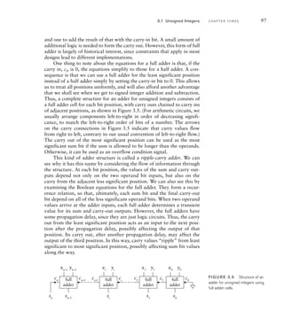
![result, which can also be interpreted as a Boolean false or true result,
respectively. This is convenient if the comparison occurs in the condition
part of an if statement, since a Boolean result is expected in that context.
It is also convenient if we want to assign the result to a net or variable,
for example:
assign gt = x y;
example 3.12 Develop a Verilog model for a thermostat that has two
8-bit unsigned binary inputs representing the target temperature and the actual
temperature in degrees Fahrenheit (˚F). Assume that both temperatures are above
freezing (32˚F). The detector has two outputs: one to turn a heater on when the
actual temperature is more than 5˚F below target, and one to turn a cooler on
when the actual temperature is more than 5˚F above target.
solution The module definition is
module thermostat ( output heater_on, cooler_on,
input [7:0] target, actual );
assign heater_on = actual target – 5;
assign cooler_on = actual target + 5;
endmodule
xn–1
gt
xn–1
yn–1
xn–1
= yn–1
xn–2
yn–2
xn–2
= yn–2
yn–1
xn–2
yn–2
x1
y1
x1…0
y1…0
xn–2…0
yn–2…0
x1
= y1
x1
y1
x0
y0
x0
y0
…
…
…
FIG U R E 3.12 A magnitude
comparator to test for greater than
inequality.
3.1 Unsigned Integers C H A P T E R T H R E E 111](https://image.slidesharecdn.com/digitaldesign-anembeddedsystemsapproachusingverilog-220525003453-7ebc98ea/85/Digital-Design-An-Embedded-Systems-Approach-Using-Verilog-pdf-132-320.jpg)
![values. The result of the * operator is an unsigned vector whose length
is the larger of the operand lengths. If we need the multiplication to be
performed with size that is the sum of the operand lengths, in order not
to overflow, we must extend the operand values before multiplying them.
For example, given the following declarations:
wire [ 7:0] x;
wire [13:0] y;
wire [21:0] p;
we could assign the product of x and y to p with the following
statement:
assign p = {14'b0, x} * {8'b0, y};
Alternatively, we could rely on Verilog’s implicit zero extension and just
write:
assign p = x * y;
Summary of Arithmetic Operations
In this section, we have examined several arithmetic operations that can
be performed on unsigned binary integers, including addition, subtrac-
tion and multiplication. We have deliberately avoided division, since it
is considerably more complex to implement than the other operations,
and arises less frequently in real-world applications. Hence, there are
relatively few application-specific digital systems that include circuits for
performing division. Division circuits are described in the books cited in
Section 3.6.
In our discussion, we focused on addition as a foundational operation
and examined a number of adder circuits that trade off between perfor-
mance and circuit area. This is a recurring theme in digital design, and is
well illustrated through consideration of adder circuits. We return to it
throughout this book.
For each operation, we also discussed how to represent the opera-
tion in Verilog models that use unsigned vectors. This approach allows
us to abstract away from the details of the digital circuits that implement
the arithmetic operations, relying on synthesis CAD tools to choose
appropriate circuits from libraries of cells that can be implemented in
3.1 Unsigned Integers C H A P T E R T H R E E 115](https://image.slidesharecdn.com/digitaldesign-anembeddedsystemsapproachusingverilog-220525003453-7ebc98ea/85/Digital-Design-An-Embedded-Systems-Approach-Using-Verilog-pdf-136-320.jpg)
![118 C H A P T E R T H R E E n u m e r i c b a s i c s
solution For the both the Gray-code input to the converter and the
binary-code output, we use vector ports. The module definition is
module gray_converter ( output reg [3:0] numeric_value,
input [3:0] gray_value );
always @*
case (gray_value)
4'b0000: numeric_value = 4'b0000;
4'b0001: numeric_value = 4'b0001;
4'b0011: numeric_value = 4'b0010;
4'b0010: numeric_value = 4'b0011;
4'b0110: numeric_value = 4'b0100;
4'b0111: numeric_value = 4'b0101;
4'b0101: numeric_value = 4'b0110;
4'b0100: numeric_value = 4'b0111;
4'b1100: numeric_value = 4'b1000;
4'b1101: numeric_value = 4'b1001;
4'b1111: numeric_value = 4'b1010;
4'b1110: numeric_value = 4'b1011;
4'b1010: numeric_value = 4'b1100;
4'b1011: numeric_value = 4'b1101;
4'b1001: numeric_value = 4'b1101;
4'b1000: numeric_value = 4'b1111;
endcase
endmodule
The module’s behavior takes the form of a truth table. It uses the Gray-code
value to select which unsigned numeric value to assign to the output.
1. How is a number x represented in binary as a sum of powers of 2?
2. What range of values can be represented as an n-bit unsigned binary
number?
3. Write a Verilog declaration for a net x to represent unsigned
numbers in the range 0 to 8191.
4. Write the binary number 01011101 in octal and in hexadecimal.
5. Resize the unsigned binary number 10010011 to 12 bits and to 6
bits. In each case, does the result correctly represent the same value
as the original number?
6. Add the two 8-bit unsigned binary numbers 01001010 and
01100000 to get an 8-bit result. Does the addition overflow?
7. What distinguishes a ripple-carry adder from a carry-lookahead
adder?
K N O W L E D G E
T E S T Q U I Z
K N O W L E D G E
T E S T Q U I Z](https://image.slidesharecdn.com/digitaldesign-anembeddedsystemsapproachusingverilog-220525003453-7ebc98ea/85/Digital-Design-An-Embedded-Systems-Approach-Using-Verilog-pdf-139-320.jpg)
![8. Write Verilog assignments to add two nets s1 and s2 of type wire
[15:0] to get a result net s3 of the same type as s1 and s2 and a
carry-out net c_out.
9. Perform the 8-bit unsigned binary subtraction 0100101001100000
to get an 8-bit result. Does the subtraction underflow?
10. Given a control signal
__
add/sub, how can we adapt an unsigned
adder to perform both addition and subtraction?
11. Write a Verilog assignment that compares two unsigned nets a and b
and assigns 1 to a net smaller if a b, or 0 otherwise.
12. How is an unsigned binary number multiplied by 16? How is it
divided by 16?
13. How many bits are required for the product of two n-bit unsigned
binary numbers?
14. Why are Gray codes often used in electromechanical position sensors?
3.2 S I G N E D I N T E G E R S
While many applications deal only with nonnegative integers, there are
others that deal with integers that range over both positive and negative
values. In this section we will explore a binary code for signed integers
and see how to implement operations on these encoded values.
3.2.1 C O D I N G S I G N E D I N T E G E R S
The predominant encoding used in digital systems for signed integers is
called 2s complement. It is a special case of radix complement representa-
tion in which the radix (the base used for positional representation) is 2. We
will refer to the Further Reference books for details of general radix comple-
ment representations, and focus our attention here just on 2s complement.
A signed number is represented in 2s-complement form as a weighted
sum of powers of two, in a similar way to unsigned binary representation.
The difference is that, for an n-bit signed number, the weight of the left-
most bit is negative. An n-bit number x represents the value
xxn12n1
xn22n2
...x020
(3.14)
This representation has a number of interesting and useful properties
that we will now explore. First, the most negative number that can be
represented has xn1 1 and all other bits 0, giving the value 2n1.
The most positive number has xn1 0 and all other bits 1, giving the
value 2n1 1. If xn1 is 1, the number represented is negative, since the
sum of all the positively weighted powers of 2 is less than 2n1. Thus,
xn1 serves as a sign bit: if it is 1, the number is negative, and if it is 0, the
3.2 Signed Integers C H A P T E R T H R E E 119](https://image.slidesharecdn.com/digitaldesign-anembeddedsystemsapproachusingverilog-220525003453-7ebc98ea/85/Digital-Design-An-Embedded-Systems-Approach-Using-Verilog-pdf-140-320.jpg)
![120 C H A P T E R T H R E E n u m e r i c b a s i c s
number is zero or positive. The range of numbers that can be represented
is not symmetric about zero, since the negation of 2n1
is one more
than the most positive number that can be represented.
example 3.14 What values are represented by the 8-bit 2s-complement
numbers 00110101 and 10110101?
solution The first number is
125
124
122
120
32164153
The second number is
127
125
124
122
120
12832164175
While 2s-complement representation for signed integers predomi-
nates, there are other forms that are useful in some applications. One form,
signed magnitude, is analogous to our conventional decimal representa-
tion for signed integers, in which we write a sequence of decimal digits for
the magnitude of a number, preceded by a or sign to indicate whether
the number is positive or negative. In signed magnitude binary representa-
tion, we represent a signed number with a sequence of binary digits (bits),
preceded by a binary code for the sign of the number. Usually, we would
encode a sign with 1 and a sign with 0. While some early digital
computers used signed magnitude representation, there are a number of
disadvantages that make it uncommon in modern digital systems. For this
reason, we will not describe in any further detail, and instead refer to the
books listed in Section 3.6, Further Reading, for more information.
Representing Signed Integers in Verilog
We saw in Section 3.1.1 that we can use vectors and built-in arithme-
tic operators to deal with unsigned integers. For signed integers, we also
use vectors, but we include the keyword signed in their declarations, for
example:
wire signed [ 7:0] a;
reg signed [13:0] b;
The arithmetic operators then assume 2s-complement representation,
with the sign bit being the left-most bit in a vector and the least significant
bit being the right-most bit.
An important point to note is that, even though we might declare nets
or variables to be unsigned or signed, the interpretation of the bits of a](https://image.slidesharecdn.com/digitaldesign-anembeddedsystemsapproachusingverilog-220525003453-7ebc98ea/85/Digital-Design-An-Embedded-Systems-Approach-Using-Verilog-pdf-141-320.jpg)
![value depends on the operator being applied and the declaration of the
other operand. If both operands to an arithmetic operation are signed, a
signed operation is performed. If either or both operations are unsigned,
an unsigned operation is performed. If we really want to interpret values
that are declared unsigned as representing signed values, we can use the
$signed conversion operation, for example:
wire [11:0] s1;
wire signed [11:0] s2;
...
assign s2 = $signed(s1); // s1 is known to be less than 2**11
Similarly, if we want to interpret values declared signed as represent-
ing unsigned values, we use the $unsigned conversion operation, for
example:
assign s1= $unsigned(s2); // s2 is known to be nonnegative
We also mentioned the abstract numeric type integer in Section 3.1.1,
showing how it can be used for nonnegative numbers. In fact, the inte-
ger type represents numbers that can be positive or negative, provided
their 2s-complement representation can fit within 32 bits. We can perform
arithmetic operations on values of type integer, and we can mix inte-
ger with unsigned and signed net and variable values. The type integer is
really just a signed variable type whose size is fixed at 32 bits.
Octal and Hexadecimal Codes for Signed Integers
We saw in Section 3.1.1 that we could use octal or hexadecimal codes
for unsigned integers. We can also use octal and hexadecimal for
2s-complement signed integers. However, when we do so, we don’t usually
think in terms of signed octal or signed hexadecimal numbers. Instead, we
just use octal or hexadecimal as a shorthand notation for the vector of
bits. We divide the vector into groups of three bits (for octal) or four bits
(for hexadecimal) and substitute the corresponding octal or hexadecimal
digit for each group.
example 3.15 The 12-bit 2s-complement representation of 84410 is
001101001100. Express the bit vector in hexadecimal.
solution Dividing into groups of four bits, we get 0011 0100 1100.
Substituting hexadecimal digits for the 4-bit groups gives 34C16.
3.2 Signed Integers C H A P T E R T H R E E 121](https://image.slidesharecdn.com/digitaldesign-anembeddedsystemsapproachusingverilog-220525003453-7ebc98ea/85/Digital-Design-An-Embedded-Systems-Approach-Using-Verilog-pdf-142-320.jpg)
![124 C H A P T E R T H R E E n u m e r i c b a s i c s
representable by the smaller number of bits. We might arrive at that
conclusion by analyzing the arithmetic operations performed to derive
the larger-sized value.
We can express sign extension of a signed value in Verilog using the
bit-replication notation to replicate the sign bit. For example given nets
declared as
wire signed [ 7:0] x;
wire signed [15:0] y;
we can write the following assignment to sign extend the value of x and
assign it to y:
assign y = {{8{x[7]}}, x};
The notation {n{...}} specifies n replications of the bits inside the inner
braces.
Sign extension or truncation of a signed value in a Verilog model
also occurs implicitly when we assign the value to a target that is
of a different length. For example, we can rewrite the above assignment
statement as
assign y = x; // x is sign-extended to 16 bits
Similarly, we can write the following assignment to truncate the value of
y and assign it to x:
assign x = y; // y is truncated to 8 bits
Negating Signed Integers
Since we can represent both positive and negative numbers using 2s-
complement encoding, it makes sense to consider negating a number. The
steps needed to perform negation of a number x are first to complement
each bit of x (that is, change each 0 to 1 and each 1 to 0), and then to
add 1. We can prove that this yields the 2s-complement representation of
x. We need to use the bit identity
_
xi1xi together with the identity in
Equation 3.17. The proof is](https://image.slidesharecdn.com/digitaldesign-anembeddedsystemsapproachusingverilog-220525003453-7ebc98ea/85/Digital-Design-An-Embedded-Systems-Approach-Using-Verilog-pdf-145-320.jpg)
![wire signed [11:0] v1, v2;
wire signed [12:0] sum ;
we can add the two 12-bit values and get a 13-bit result using the
assignment
assign sum = {v1[11], v1} + {v2[11], v2};
Alternatively, we can rely on Verilog’s implicit sign extension, given that
the assignment target is 13 bits, and just write:
assign sum = v1 + v2;
Developing a Verilog model that represents the sum using the same
number of bits as the operands and that derives the overflow condition is
somewhat more involved. Referring back to our case analysis of the signs
of the operands, we see that overflow only occurs if both operands are
nonnegative and the carry in to the sign position is 1 (yielding an appar-
ently negative result), or if both operands are negative and the carry in to
the sign position is 0 (yielding an apparently nonnegative result). Given
this observation and the declarations
wire signed [7:0] x‚ y, z;
wire ovf;
we can write the following assignments to derive the required sum and
overflow condition bit:
assign z = x + y;
assign ovf = ~x[7] ~y[7] z[7] | x[7] y[7] ~z[7];
Subtraction of Signed Integers
Now that we have seen how to perform addition and negation on
2s-complement numbers, subtraction follows from the identity
xyx(y)x
_
y1
3.2 Signed Integers C H A P T E R T H R E E 127](https://image.slidesharecdn.com/digitaldesign-anembeddedsystemsapproachusingverilog-220525003453-7ebc98ea/85/Digital-Design-An-Embedded-Systems-Approach-Using-Verilog-pdf-148-320.jpg)
![128 C H A P T E R T H R E E n u m e r i c b a s i c s
y0
y1
yn–1
y0
c0
cn
y1
yn–1
…
…
…
…
x0
x1
xn–1
x0
x1
xn–1
… s0
s1
sn–1
sn–1
/dn–1
s1
/d1
s0
/d0
…
cn–1
adder
add/sub
unsigned
ovf/und
signed
ovf
FIG U R E 3.18 An adder/
subtracter for both unsigned and
2s-complement numbers.
This suggests that we can use the same adder/subtracter, shown in
Figure 3.9, that we described for unsigned numbers. The revised form
that deals with both kinds of numbers, unsigned and 2s-complement, is
shown in Figure 3.18. For signed numbers, when the
__
add/sub control
input is 0, the y operand is passed through the XOR gates unchanged
and the carry in to the adder is 0. When the
__
add/sub input is 1, the y
operand is complemented by the XOR gates, and the carry in is 1. Thus
the circuit subtracts by adding to x the complement of y and 1. Depending
on whether the operands are interpreted as unsigned or signed operands,
we use one or the other of the overflow condition outputs.
In Verilog, we express subtraction of signed values using the operator.
For signed values, if we want to allow for a result that would overflow if rep-
resented as the same number of bits as the operands, we can resize the oper-
and values, as we described for signed addition. Thus, given the declarations
wire signed [11:0] v1, v2;
wire signed [12:0] diff;
we can calculate the 13-bit difference between the two 12-bit values using
the assignment
assign diff = {v1[11], v1} – {v2[11], v2};
or in simplified form, relying on Verilog’s implicit sign extension,
assign diff = v1 – v2;](https://image.slidesharecdn.com/digitaldesign-anembeddedsystemsapproachusingverilog-220525003453-7ebc98ea/85/Digital-Design-An-Embedded-Systems-Approach-Using-Verilog-pdf-149-320.jpg)
![Again, a Verilog model that represents the difference using the same
number of bits as the operands and that derives the overflow condition is
somewhat more involved. Since xy is the same as x(y), and the sign
of y is the complement of the sign of y (except when y is zero), we can
work out the overflow condition by examining sign bits in a way similar
to that for addition. We just need to use the logical negation of the sign bit
of y in the overflow expression. Thus, for the declarations
wire signed [7:0] x, y, z;
wire ovf;
we can write the following assignments to derive the required difference
and overflow condition bit:
assign z = x – y;
assign ovf = ~x[7] y[7] z[7] | x[7] ~y[7] ~z[7];
The case of y being zero is handled correctly by this expression, since in
that case, the result z is the same as x, and so the sign of z is the same as
the sign of x.
A further case to consider is subtraction of two unsigned numbers
to give a signed result, rather than underflowing when the difference is
negative. In order to determine the size to use for the result, we can con-
sider the range of possible result values. Suppose we are subtracting n-bit
unsigned values. The greatest result arises from subtraction of zero from
the greatest unsigned value, giving 2n
1. The least (most negative) result
arises from subtraction of 2n
1 from zero, giving 2n
1. This range is
encompassed by a result with n1 bits. So the simplest way to express
the subtraction is to zero extend the operands by one bit, treat them as
signed, and then apply the signed subtraction operation. In Verilog, given
8-bit operands and a 9-bit result declared as
wire [7:0] v1, v2;
wire signed [8:0] diff;
we could write the subtraction as
assign diff = $signed({1'b0, v1}) – $signed({1'b0, v2});
3.2 Signed Integers C H A P T E R T H R E E 129](https://image.slidesharecdn.com/digitaldesign-anembeddedsystemsapproachusingverilog-220525003453-7ebc98ea/85/Digital-Design-An-Embedded-Systems-Approach-Using-Verilog-pdf-150-320.jpg)
![module fixed_converter ( input [5:–7] in,
output signed [7:–7] out );
assign out = {2'b0, in};
endmodule
In our discussion of integers, we mentioned that Verilog provides the
type integer for abstract representation of numbers. Unfortunately, Veri-
log does not provide a corresponding type for abstract representation of
fixed-point numbers. Abstract fixed-point types could, in principle, be
included in the language, as has been done in the Ada programming lan-
guage, for example. While we might hope that abstract fixed-point types
might be included in a future version of Verilog as applications become
more common, for now, we will just make use of the vector types.
For testbenches in Verilog, however, we can make use of a built-in
type real. We can declare a variable (but not a net) to be of this type as
follows:
real x;
Real variables are actually represented using floating-point format,
described in Section 3.4. However, we can use them for nonintegral val-
ues to be applied to the inputs or checked at the outputs of models using
fixed-point representation. Some examples are
real r1, r2;
wire [5:-16] x, y;
wire [8:-14] z;
r1 = $itor(x)/2**16;
r2 = r1 / ($itor(y)/2**16);
z = $rtoi(r2 * 2**14);
The conversion function $itor used here converts from a vector value,
interpreted as an integer, to a real-number value. The scaling is required,
since our actual interpretation of the vector is a fixed-point value. The
conversion function $rtoi works in the reverse direction, from a real-
number value to a vector interpreted as an integer. Again, scaling is
required to take account of our actual interpretation of the vector as a
fixed-point value.
3.3 Fixed-Point Numbers C H A P T E R T H R E E 135](https://image.slidesharecdn.com/digitaldesign-anembeddedsystemsapproachusingverilog-220525003453-7ebc98ea/85/Digital-Design-An-Embedded-Systems-Approach-Using-Verilog-pdf-156-320.jpg)
![just perform the operations assuming the right-most bits of the operands
are the corresponding least significant bits. If both operands are declared
with the same index bounds, the operations are performed correctly for
the fixed-point interpretation of the values. If, however, the index bounds
are not the same, we need to extend or truncate both ends of the operands
to make sure that the assumed binary points align.
example 3.22 Write Verilog declarations and an assignment to perform
the addition described in Example 3.21.
solution The declarations for the nets a, b and c are
wire signed [3:-7] a;
wire signed [5:-4] b, c;
We could try the following assignment as a first attempt:
assign c = a + b;
Since a is 11 bits and b is 10 bits, the operator would sign extend b to 11 bits
and perform an 11-bit addition. The implicit binary points would be misaligned
by three places. To correct this, we need to sign extend the value of a by 2
bits, and to truncate the 3 least signficant bits of a. We can use a part select to
perform the truncation, but the result of a part select is treated as unsigned in
Verilog. We can use the $signed conversion operation to re-interpret it as signed.
The following assignment incorporates these corrections:
assign c = {{2{a[3]}}, $signed(a[3:–4])} + b;
Another related issue to be aware of is the position of the binary point
in the result of a multiplication. We can appeal to the way in which we
do multiplication of decimals for an analogy. Suppose, for example, that
we wish to multiply 23.76 by 3.128. We first multiply the digits without
regard to the decimal points to get 7432128. We then add the number of
post-decimal digits in the operands, namely, 2 and 3, to get the number of
post-decimal digits in the result, namely, 5. Thus the product is 74.32128.
Byanalogy,multiplyingtwofixed-pointbinarynumberswithm1 andm2
pre-binary-point bits and f1 and f2 post-binary-point bits, respectively, gives
us a product with m1m2 pre-binary-point bits and f1f2 post-binary-
point bits. For example, multiplying 1.1012 by 10.12 gives 100.00012. If
3.3 Fixed-Point Numbers C H A P T E R T H R E E 137](https://image.slidesharecdn.com/digitaldesign-anembeddedsystemsapproachusingverilog-220525003453-7ebc98ea/85/Digital-Design-An-Embedded-Systems-Approach-Using-Verilog-pdf-158-320.jpg)
![138 C H A P T E R T H R E E n u m e r i c b a s i c s
we are to use the Verilog * operator to produce a product of this length, we
must extend each operand on the left to the final product size.
1. How is a nonnegative number x represented as a sum of powers of
2 in fixed-point form?
2. What range of values can be represented as signed fixed-point
numbers with m pre-binary-point bits and f post-binary-point bits?
3. Write a Verilog declaration for a net x, not to represent numbers in
the range 0.0 to 359.9 with a precision of 0.1.
4. Write a Verilog assignment to subtract the value of a net s2 from the
value of a net s1, where both are of type wire [7:–7], to get a result
net s3 of the same type. No overflow detection is required.
5. How many bits are required for the product of two fixed-point
numbers with 5 pre-binary-point bits and 9 post-binary-point bits?
3.4 F LO AT I N G - P O I N T N U M B E R S
The final number representation that we will discuss in this chapter is
floating-point, which is another representation for approximating real
numbers. They allow for representation of a greater range of numbers
than a fixed-point representation with the same number of bits. However,
implementation of arithmetic operations is considerably more complex.
Indeed, most circuits for floating-point arithmetic are not combinational,
since they would otherwise be too complex and reduce overall system per-
formance. Since we have deferred detailed discussion of sequential circuit
design to a later chapter, we will not go into circuits for floating-point
arithmetic here. For completeness of our survey of numeric representa-
tions in this chapter, we will just introduce floating-point format. Unfor-
tunately, Verilog only provides rudimentary features for dealing with
floating-point numbers. They are not sufficient for modeling floating-
point circuits, so we will not discuss them here.
3.4.1 C O D I N G F LO AT I N G - P O I N T N U M B E R S
Floating-point representation in digital systems is based on the same ideas
as scientific notation for decimal numbers. We can write numbers that are
very small or very large as the product of a fixed-point decimal fraction and
a power of 10. This saves us from writing long strings of leading or trailing
zeros and makes the number much easier to read and understand. Exam-
ples of numbers expressed in scientific notation are 6.022141991023
(Avogadro’s number) and 1.602176531019 (the charge, in Coulombs,
of an electron). We call the fractional part before thesign the mantissa
and the power to which 10 is raised the exponent.
K N O W L E D G E
T E S T Q U I Z
K N O W L E D G E
T E S T Q U I Z](https://image.slidesharecdn.com/digitaldesign-anembeddedsystemsapproachusingverilog-220525003453-7ebc98ea/85/Digital-Design-An-Embedded-Systems-Approach-Using-Verilog-pdf-159-320.jpg)


![bottom of Figure 4.4. This arrangement is called a pipeline, as it allows
data and intermediate results to flow through over several clock cycles.
A new input value arrives at the beginning of each clock cycle. During
a clock cycle, each subcircuit uses the value from the preceding regis-
ter (or from the input, in the case of the first subcircuit) to perform its
combinational function and to yield an intermediate result. On the next
rising clock edge, the intermediate results are stored in the registers at the
outputs of the subcircuits. Each intermediate result is then used by the next
subcircuit during the next clock cycle. Computation is thus performed in
assembly-line fashion. A new final result reaches the output on each clock
edge, having taken several clock cycles to be computed.
example 4.1 Develop a Verilog model for a pipelined circuit that com-
putes the average of corresponding values in three streams of input values, a, b
and c. The pipeline consists of three stages: the first stage sums values of a and
b and saves the value of c; the second stage adds on the saved value of c; and
the third stage divides by three. The inputs and output are all signed fixed-point
numbers indexed from 5 down to 8.
solution The module definition is
module average_pipeline ( output reg signed [5:–8] avg,
input signed [5:–8] a, b, c,
input clk );
wire signed [5:–8] a_plus_b, sum, sum_div_3;
reg signed [5:–8] saved_a_plus_b, saved_c, saved_sum;
assign a_plus_b = a + b;
always @(posedge clk) begin // Pipeline register 1
saved_a_plus_b = a_plus_b;
saved_c = c;
end
assign sum = saved_a_plus_b + saved_c;
always @(posedge clk) // Pipeline register 2
saved_sum = sum;
assign sum_div_3 = saved_sum * 14'b00000001010101;
always @(posedge clk) // Pipeline register 3
avg = sum_div_3;
endmodule
154 C H A P T E R F O U R s e q u e n t i a l b a s i c s](https://image.slidesharecdn.com/digitaldesign-anembeddedsystemsapproachusingverilog-220525003453-7ebc98ea/85/Digital-Design-An-Embedded-Systems-Approach-Using-Verilog-pdf-175-320.jpg)
![We have included the reset input in the event list of the block, since the
block may need to update the outputs on a change of value of the reset
input, not just on a change of value of the clock input. The revised block
checks the value of the reset input first, before it looks at the clock input.
If the reset input is 1, the block clears the output immediately. Only if the
reset input is 0 does the block proceed to check for activity of the syn-
chronous control input on a rising clock edge. As before, we can change
the assignment to the output to reflect the difference between a single-bit
flip-flop and a multibit register.
example 4.2 Develop a Verilog model for an accumulator that calculates
the sum of a sequence of fixed-point numbers. Each input number is signed with
4 pre-binary-point and 12 post-binary-point bits. The accumulated sum has 8
pre-binary-point and 12 post-binary-point bits. A new number arrives at the
input during a clock cycle when the data_en control input is 1. The accumulated
sum is cleared to 0 when the reset control input is 1. Both control inputs are
synchronous.
solution The module requires a clock input, two control inputs, a data
input and a data output, as follows:
module accumulator
( output reg signed [7:-12] data_out,
input signed [3:-12] data_in,
input data_en, clk, reset );
wire signed [7:-12] new_sum;
assign new_sum = data_out + data_in;
always @(posedge clk)
if (reset) data_out = 20'b0;
else if (data_en) data_out = new_sum;
endmodule
The first assignment in the module models the addition of the accumulated
sum (data_out) and the data input. The data input is implicitly sign-extended to
match the size of the sum. The always block models the register used to accumu-
late the sum. It is based on the template for a register with synchronous reset and
clock enable. When reset is 1, the block clears the register output, represented by
the output variable data_out. If reset is 0, the block checks whether a new data
value has arrived and been added to the sum. In that case, the register output is
updated with the new sum; otherwise, it is unchanged.
4.1 Storage Elements C H A P T E R F O U R 159](https://image.slidesharecdn.com/digitaldesign-anembeddedsystemsapproachusingverilog-220525003453-7ebc98ea/85/Digital-Design-An-Embedded-Systems-Approach-Using-Verilog-pdf-180-320.jpg)

![example 4.7 Develop a Verilog model of the circuit from Example 4.6.
solution The module definition is
module decoded_counter ( output ctrl,
input clk );
reg [3:0] count_value;
always @(posedge clk)
count_value = count_value + 1;
assign ctrl = count_value == 4'b0111 ||
count_value == 4'b1011;
endmodule
The module contains an always block that represents the counter. It is similar
in form to a block for an edge-triggered register. The difference is that the value
assigned to the count_value output on a rising clock edge is the incremented
count value. The assignment to count_value represents the update of the value
stored in the register, and the addition of 1 represents the incrementer. The final
assignment statement in the module represents the decoder.
The counter that we have described so far is free running, increment-
ing the count value on every clock cycle. We can modify the counter to
make it useful in applications that require more control over the count
value. Two simple modifications involve adding a clock enable and a
reset input to the storage register within a counter. The clock-enable input
allows us to control when the counter increments its value, so this input
is often called a count-enable input. The reset input allows us to clear
the count value back to zero. A counter modified in this way is shown in
Figure 4.22. This form of counter is very useful for counting occurrences
of events. We would connect a signal indicating event occurrence to the
count-enable input of the counter. If we need to count events over several
intervals, we can reset the counter at the start of each interval.
Another modification is a terminal-count output. This is simply a
decoded output that is 1 when the counter reaches is maximum, or ter-
minal, value. For the counters we have described above, the maximum
value of 2n
1 is represented by a count value with all 1 bits. We can use
an n-input AND gate to generate the terminal count output, as shown in
Figure 4.23. For a free-running counter, the terminal-count output is 1
for a single clock cycle every 2n
clock cycles; that is, it is a periodic signal
whose frequency is the input clock frequency divided by 2n
.
4.2 Counters C H A P T E R F O U R 169
+1
Q
clk
CE
reset
D
CE
Q
reset
clk
FIG U R E 4.22 A counter with
clock-enable and reset inputs.
counter
…
…
Q0
Q1
Qn
…
TC
clk
FIG U R E 4.23 A counter with
terminal-count output.](https://image.slidesharecdn.com/digitaldesign-anembeddedsystemsapproachusingverilog-220525003453-7ebc98ea/85/Digital-Design-An-Embedded-Systems-Approach-Using-Verilog-pdf-190-320.jpg)
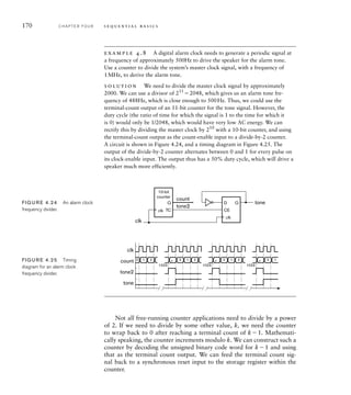
![example 4.9 Design a circuit for a modulo 10 counter, otherwise known
as a decade counter.
solution The maximum count value is 9, so we need 4 bits for the counter.
The unsigned binary code word for 9 is 10012. We can decode this value and
use it to reset to counter to 0 on the next clock cycle. The circuit is shown in
Figure 4.26.
4.2 Counters C H A P T E R F O U R 171
clk Q0
Q1
Q2
Q3
Q0
Q1
Q2
Q3
reset
counter
clk
FIG U R E 4.26 A decade
counter.
example 4.10 Develop a Verilog model for the decade counter of
Example 4.9.
solution The module definition is
module decade_counter ( output reg [3:0] q,
input clk );
always @(posedge clk)
q = q == 9 ? 0 : q + 1;
endmodule
We model the output port for the count value using an unsigned vector, since
it is represents a binary-coded integer value. On a rising clock edge, the always
block checks whether the counter has reached the terminal count value. If so,
the count value wraps back to 0; otherwise, the block adds 1 to yield the new
count value.
Another form of counter that is useful in timing applications is a
down counter with load. This counter is loaded with an input value, and
then decrements the count value. The terminal count output is activated
when the count value reaches zero. A circuit for the counter is shown in
Figure 4.27. It consists of a register whose input comes either from the
input value to be loaded or from the decremented count value. In this
case, the loading of input data is synchronous, since it occurs on a rising
clock edge.](https://image.slidesharecdn.com/digitaldesign-anembeddedsystemsapproachusingverilog-220525003453-7ebc98ea/85/Digital-Design-An-Embedded-Systems-Approach-Using-Verilog-pdf-192-320.jpg)
![172 C H A P T E R F O U R s e q u e n t i a l b a s i c s
If the clock input to the counter is a periodic signal with period t and
the counter is loaded with a value k, the terminal count is reached after
an interval of kt. Thus, this form of counter can be used as an interval
timer, where the terminal-count output signal is used to trigger an activity
after expiration of a given time interval.
example 4.11 Develop a Verilog model for an interval timer that has
clock, load and data input ports and a terminal-count output port. The timer
must be able to count intervals of up to 1000 clock cycles.
solution The data input and counter need to be 10 bits wide, since that is
the minimum number of bits needed to represent 1000. The module definition is
module interval_timer_rtl ( output tc,
input [9:0] data,
input load, clk );
reg [9:0] count_value;
always @(posedge clk)
if (load) count_value = data;
else count_value = count_value – 1;
assign tc = count_value == 0;
endmodule
On a rising clock edge, the always block uses the load input to determine
whether to update the count value with the data input or the decremented
count value. The decrement operation is performed using an unsigned subtrac-
tion without borrow out. So after reaching zero, the count value wraps back to
the largest 10-bit value, namely, 1023. The final assignment in the architecture
drives the terminal count to 1 when the count value reaches zero.
example 4.12 Modify the interval timer so that, when it reaches zero, it
reloads the previously loaded value rather than wrapping around to the largest
count value.
D Q
–1
=0?
Q
TC
clk
load
D
0
1
clk
FIG U R E 4.27 A down
counter with synchronous load.](https://image.slidesharecdn.com/digitaldesign-anembeddedsystemsapproachusingverilog-220525003453-7ebc98ea/85/Digital-Design-An-Embedded-Systems-Approach-Using-Verilog-pdf-193-320.jpg)
![solution We need to use a separate register to store the data value to load
into the counter. When the load input is activated, a new data value is loaded
into the storage register as well as into the counter. When the terminal count is
reached, the counter should be loaded from the storage register. The inputs and
outputs of the revised interval timer are the same, so we don’t need to change the
ports of the module definition. The revised module is
module interval_timer_repetitive ( output tc,
input [9:0] data,
input load, clk );
reg [9:0] load_value, count_value;
always @(posedge clk)
if (load) begin
load_value = data;
count_value = data;
end
else if (count_value == 0)
count_value = load_value;
else
count_value = count_value – 1;
assign tc = count_value == 0;
endmodule
In this module, we have added a separate variable, load_value, to represent the
storage register. The always block is revised so that, when load is 1 on a ris-
ing clock edge, both the load_value variable and the count_value variable are
updated from the data input. Also, when the count value is 0 on a rising clock
edge (provided load is not 1), the count value is updated from the load_value
variable. Otherwise, the count value is decremented as before.
The last kind of counter that we will describe in this section is a ripple
counter (distinct from ripple carry used in an incrementer of a counter),
shown in Figure 4.28. It is somewhat different in structure from the syn-
chronous counters we have previously examined. Like those counters, it
has a collection of flip-flops for storing the count value. However, unlike
them, the clock signal is not connected in common to all of the flip-flop
clock inputs. Rather, the clock input just triggers the flip-flop for the
least significant bit, causing it to toggle between 0 and 1 on each rising
clock edge. When the Q output changes to 0, the
_
Q output changes to
1, triggering the next flip-flop to toggle between 0 and 1. This flip-flop
behaves similarly, causing the third flip-flop to toggle when it (the second
4.2 Counters C H A P T E R F O U R 173
D
Q
Q
D
Q
Q
D
Q
Q
D
Q
Q
Q0
Q1
Q2
Qn
clk clk
clk
clk
clk
FIG U R E 4.28 Structure of a
ripple counter.](https://image.slidesharecdn.com/digitaldesign-anembeddedsystemsapproachusingverilog-220525003453-7ebc98ea/85/Digital-Design-An-Embedded-Systems-Approach-Using-Verilog-pdf-194-320.jpg)
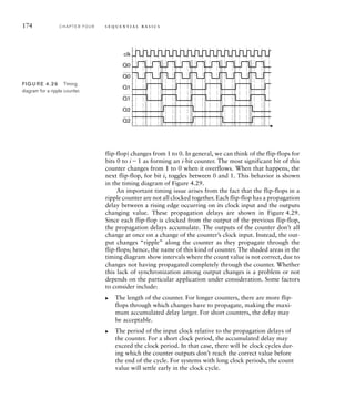
![In the diagram, the signals upon which data flows are drawn with thicker lines,
since they carry multibit binary-coded values. The remaining signals, drawn with
lighter weight lines, are the clock and the control signals. They include select
signals for the multiplexers, clock-enable signals for the registers, and a signal
to choose the operation to be performed by the adder/subtracter. The values of
the control signals are driven by a separate control section, not shown on the
diagram.
example 4.14 Develop a Verilog model of the complex multiplier
datapath.
solution The module includes ports for the data inputs and outputs, as
well as clock and reset inputs and an input to indicate the arrival of new data.
We will return to the last of these inputs later. The module definition is
4.3 Sequential Datapaths and Control C H A P T E R F O U R 177
0
1
0
1
D
CE
Q
D
CE
Q
× ±
D
CE
Q
D
CE
Q
p_r
p_i
a_r
a_i
b_r
b_i
a_sel
b_sel
pp1_ce
pp2_ce
sub
p_r_ce
p_i_ce
clk
clk
clk clk
clk
FIG U R E 4.30 Datapath for a
sequential complex multiplier.
module multiplier
( output reg signed [7:-24] p_r, p_i,
input signed [3:-12] a_r, a_i, b_r, b_i,
input clk, reset, input_rdy );
reg a_sel, b_sel, pp1_ce, pp2_ce, sub, p_r_ce, p_i_ce;
wire signed [3:-12] a_operand, b_operand;
wire signed [7:-24] pp, sum;
reg signed [7:-24] pp1, pp2;
...
(continued)
To form the imaginary part, two partial products are added. In each case, the
part of the complex product is stored in an output register.](https://image.slidesharecdn.com/digitaldesign-anembeddedsystemsapproachusingverilog-220525003453-7ebc98ea/85/Digital-Design-An-Embedded-Systems-Approach-Using-Verilog-pdf-198-320.jpg)
![178 C H A P T E R F O U R s e q u e n t i a l b a s i c s
The nets and variables declared within the module represent the control signals
and the internal data connections. There are further declarations for the control
section that we will return to later. In the statement part of the architecture, the
assignments to a_operand and b_operand represent the multiplexers, and the
assignment to pp represents the multiplier. (The multiplier operands are extended
so that the result size matches the sizes of the real and imaginary parts of the
product.) The first two always blocks represent the partial-product registers. The
assignment to sum represents the adder/subtracter, and the second two always
blocks represent the output registers. We will return to further statements that
represent the control section later.
example 4.15 Design a control sequence for the control signals of the
sequential complex multiplier.
solution We first need to determine a sequence of operations to be
performed by the datapath to implement the required function expressed in
Equation 4.1. There are many possible sequences, but we must ensure that there
is no conflict for resources; that is, we must ensure that we don’t try to use an
element of the datapath for more than one operation at a time. One possible
sequence, initiated by input_rdy being 1, is:
1. Multiply a_r and b_r, and store the result in partial product register 1.
2. Multiply a_i and b_i, and store the result in partial product register 2.
assign a_operand = ~a_sel ? a_r : a_i;
assign b_operand = ~b_sel ? b_r : b_i;
assign pp = {{4{a_operand[3]}}, a_operand, 12'b0} *
{{4{b_operand[3]}}, b_operand, 12'b0};
always @(posedge clk) // Partial product 1 register
if (pp1_ce) pp1 = pp;
always @(posedge clk) // Partial product 2 register
if (pp2_ce) pp2 = pp;
assign sum ~sub ? pp1 + pp2 : pp1 – pp2;
always @(posedge clk) // Product real-part register
if (p_r_ce) p_r = sum;
always @(posedge clk) // Product imaginary-part register
if (p_i_ce) p_i = sum;
...
endmodule](https://image.slidesharecdn.com/digitaldesign-anembeddedsystemsapproachusingverilog-220525003453-7ebc98ea/85/Digital-Design-An-Embedded-Systems-Approach-Using-Verilog-pdf-199-320.jpg)
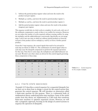
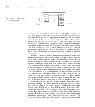
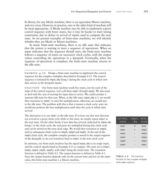
![182 C H A P T E R F O U R s e q u e n t i a l b a s i c s
An important issue to consider when designing a finite-state machine
is how to encode the state values. We glossed over that in Example 4.16
by treating the states as abstract values. As we discussed in Chapter 2,
if we have N states, we need at least ⎡log2 N⎤ bits in our code. However,
we may choose to have more if that simplifies circuitry that uses encoded
states. In particular, while a longer than minimal code length requires
more flip-flops in the state register and more wires for the state signals,
it may make the next-state and output logic circuits simpler and smaller.
In general choosing an optimal state encoding is a complex mathematical
problem. However, synthesis CAD tools incorporate methods for choos-
ing a state encoding, so we may be able to let a tool make the choice for
us. One aspect of state encoding is the choice of a code word to represent
the initial state. In many cases, a good choice is a code word with all 0
bits, since that allows us to use a simple register with reset for the state
register. If some other code word is chosen for the initial state, that code
word must be loaded into the register on system reset.
Modeling Finite-State Machines in Verilog
Since a finite-state machine is composed of a register, next-state logic and
output logic, a straightforward way to model a finite-state machine is
to use the Verilog features that we already know for modeling registers
and combinational logic. The only aspect we have not addressed is how
to represent the state set, particularly when we want to take an abstract
view and leave state encoding to the synthesis tool. In Verilog, we can use
parameter definitions to specify a set of symbolic names associated with
the binary code words for the states. For example, we can define param-
eters for the states in Example 4.16 as follows:
parameter [2:0] step1 = 3'b000, step2 = 3'b001,
step3 = 3'b010, step4 = 3'b011,
step5 = 3'b100;
This defines five parameters, named step1 through step5, corresponding
to the binary code words 000 through 100, respectively. In the rest of the
state machine model, we just use the symbolic names, not the code word
values. A synthesis tool may be able to recode the state parameters, that is,
to choose an alternate encoding for the state set, to optimize the generated
hardware for the state machine.
We can declare a variable to represent the current state of a state
machine as follows:
reg [2:0] current_state;](https://image.slidesharecdn.com/digitaldesign-anembeddedsystemsapproachusingverilog-220525003453-7ebc98ea/85/Digital-Design-An-Embedded-Systems-Approach-Using-Verilog-pdf-203-320.jpg)
![This specifies that current_state is a vector that can take on parameter
values representing states. So, for example, we could make the following
assignment in a procedural block:
current_state = step4;
to assign the value step4 to the variable.
example 4.17 Develop a Verilog model of the finite-state machine in
Example 4.16.
solution We will augment the architecture declaration of Example 4.14
with the Verilog representation of the control section. The additional declarations
of parameters for the set of states and variables for the current and next state are
parameter [2:0] step1 = 3'b000, step2 = 3'b001,
step3 = 3'b010, step4 = 3'b011,
step5 = 3'b100;
reg [2:0] current_state, next_state ;
4.3 Sequential Datapaths and Control C H A P T E R F O U R 183
The additional statements added to the module are
always @(posedge clk or posedge reset) // State register
if (reset) current_state = step1;
else current_state = next_state;
always @* // Next-state logic
case (current_state)
step1: if (!input_rdy) next_state = step1;
else next_state = step2;
step2: next_state = step3;
step3: next_state = step4;
step4: next_state = step5;
step5: next_state = step1;
endcase
always @* begin // Output_logic
a_sel = 1'b0; b_sel = 1'b0; pp1_ce = 1'b0; pp2_ce = 1'b0;
sub = 1'b0; p_r_ce = 1'b0; p_i_ce = 1'b0;
case (current_state)
step1: begin
pp1_ce = 1'b1;
end
(continued)](https://image.slidesharecdn.com/digitaldesign-anembeddedsystemsapproachusingverilog-220525003453-7ebc98ea/85/Digital-Design-An-Embedded-Systems-Approach-Using-Verilog-pdf-204-320.jpg)
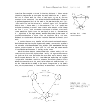
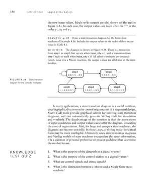
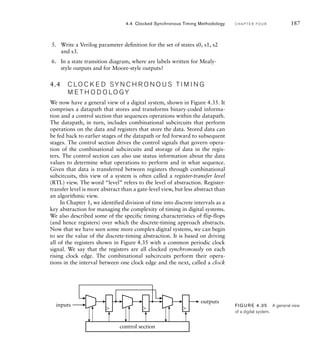
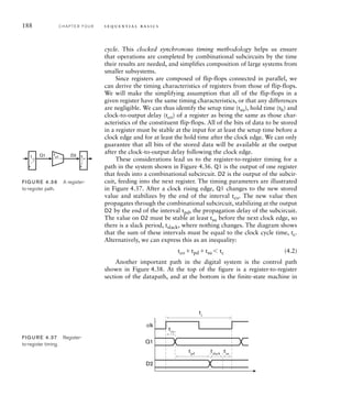
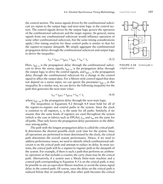
![It uses an RS-latch with negative-logic inputs and a double-throw switch.
When the switch is in the position shown, it holds the reset input of the
latch active, producing a 0 at the Q output. When the switch is toggled,
we assume that one contact is opened before the other contact is closed.
(This is sometimes called “break before make.”) Bouncing on the con-
tact to be opened simply leaves the latch in the reset state. When the
first bounce occurs on the contact to be closed, the set input is activated,
causing the Q output to change to 1. Subsequent bounces leave the latch
in the set state. The behavior is similar when the switch is toggled in the
other direction.
While this approach is very effective, it has two drawbacks. First,
it requires two inputs to the digital system for what is really just one
input. Second, it requires a double-throw switch, whereas many low-cost
applications require a single-throw switch consisting of two contacts that
are shorted together by a push button. Simple circuits for debouncing
single-throw switches generally rely on analog circuit design techniques
and require components external to the main digital chip. We will not
discuss them here, but refer to Section 4.6, Further Reading. Instead, we
will outline a fully digital approach to debouncing that can be designed
into the main digital circuit of a system.
A simple way of connecting a single-throw or momentary-contact
switch to a digital circuit input is shown in Figure 4.46. When the switch
is open, the input is pulled to 1, and when the switch is closed, the input
is pulled to 0. A change of switch position causes the input to toggle
between 0 and 1 until the bouncing stops and the input settles at its final
value. Rather than using the input value directly within the system, we
sample it at intervals longer than the bounce time. When we get two suc-
cessive samples that have the same value, we use that value as the stable
state of the switch input.
example 4.20 Develop a Verilog model of a debouncer for a push-
button switch that uses a debounce interval of 10ms. Assume the system clock
frequency is 50MHz.
solution The module definition is
4.4 Clocked Synchronous Timing Methodology C H A P T E R F O U R 195
+V
FIG U R E 4.46 Simple switch
input connection.
module debouncer ( output reg pb_debounced,
input pb,
input clk, reset );
reg [18:0] count500000; // values are in the range
// 0 to 499999
wire clk_100Hz;
reg pb_sampled;
(continued)](https://image.slidesharecdn.com/digitaldesign-anembeddedsystemsapproachusingverilog-220525003453-7ebc98ea/85/Digital-Design-An-Embedded-Systems-Approach-Using-Verilog-pdf-216-320.jpg)
![198 C H A P T E R F O U R s e q u e n t i a l b a s i c s
wire signed [3:–12] a_r, a_i, b_r, b_i;
wire signed [7:–24] p_r, p_i;
real real_a_r, real_a_i, real_b_r, real_b_i,
real_p_r, real_p_i, err_p_r, err_p_i;
task apply_test ( input real a_r_test, a_i_test,
b_r_test, b_i_test );
begin
real_a_r = a_r_test; real_a_i = a_i_test;
real_b_r = b_r_test; real_b_i = b_i_test;
input_rdy = 1'b1;
@(negedge clk) input_rdy = 1'b0;
repeat (5) @(negedge clk);
end
endtask
multiplier duv ( .clk(clk), .reset(reset),
.input_rdy(input_rdy),
.a_r(a_r), .a_i(a_i),
.b_r(b_r), .b_i(b_i),
.p_r(p_r), .p_i(p_i) );
always begin // Clock generator
#(t_c/2) clk = 1'b1;
#(t_c – t_c/2) clk = 1'b0;
end
initial begin // Reset generator
reset = 1'b1;
#(2*t_c) reset = 1'b0;
end
initial begin // Apply test cases
@(negedge reset)
@(negedge clk)
apply_test(0.0, 0.0, 1.0, 2.0);
apply_test(1.0, 1.0, 1.0, 1.0);
// further test cases ...
$finish;
end
assign a_r = $rtoi(real_a_r * 2**12);
assign a_i = $rtoi(real_a_i * 2**12);
assign b_r = $rtoi(real_b_r * 2**12);
assign b_i = $rtoi(real_b_i * 2**12);
always @(posedge clk) // Check outputs
if (input_rdy) begin
real_p_r = real_a_r * real_b_r – real_a_i * real_b_i;
(continued)](https://image.slidesharecdn.com/digitaldesign-anembeddedsystemsapproachusingverilog-220525003453-7ebc98ea/85/Digital-Design-An-Embedded-Systems-Approach-Using-Verilog-pdf-219-320.jpg)


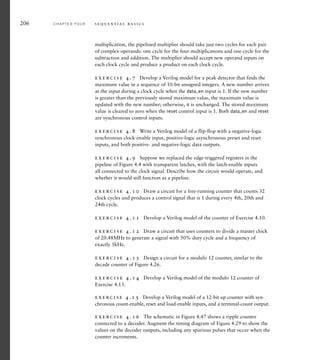
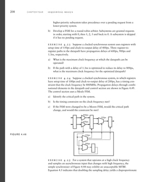

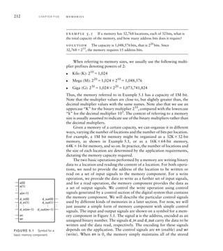
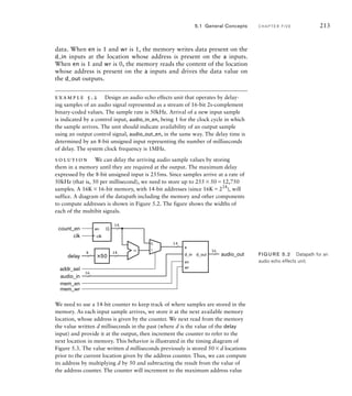
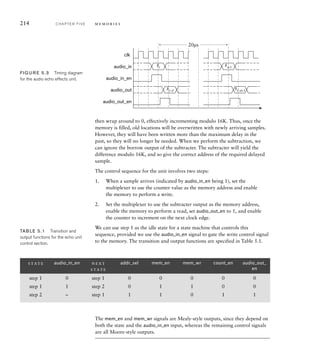
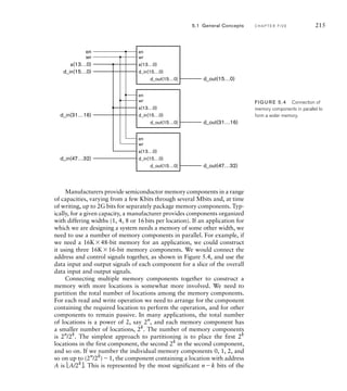
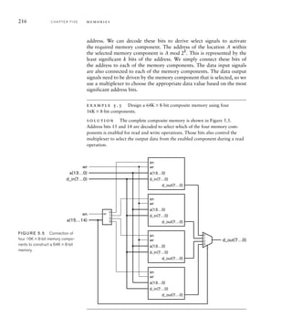
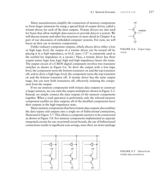
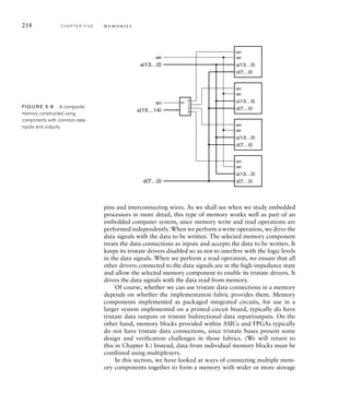
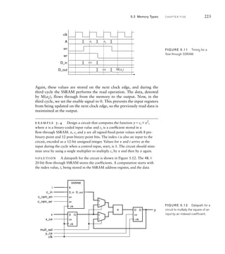
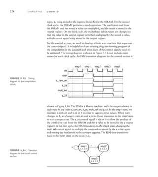
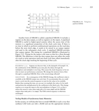
![226 C H A P T E R F I V E m e m o r i e s
resources provided in the target implementation fabric. We saw in Chapter 4
that to model a register, we declare a variable to represent the stored regis-
ter value and assign a new value to it on a rising clock edge. We can extend
this approach to model an SSRAM in Verilog. We need to declare a vari-
able that represents all of the locations in the memory. The way to do this
is to declare an array variable, which represents a collection of values, each
with an index that corresponds to its location in the array. For example, to
model a 4K16-bit memory, we would write the following declaration:
reg [15:0] data_RAM [0:4095];
The declaration specifies a variable named data_RAM that is an array with
elements index from 0 to 4095. Each element is a 16-bit vector.
Once we have declared the variable representing the storage, we write
an always block that performs the write and read operations. The block
is similar in form to that for a register. For example, an always block to
model a flow-through SSRAM based on the variable declaration above is
always @(posedge clk)
if (en)
if (wr) begin
data_RAM[a] = d_in; d_out = d_in;
end
else
d_out = data_RAM[a];
On a rising clock edge, the block checks the enable input, and only per-
forms an operation if it is 1. If the write control input is 1, the block
updates the element of the data_RAM signal indexed by the address using
the data input. The block also assigns the data input to the data output,
representing the flow-through that occurs during a write operation. If the
write control input is 0, the block performs a read operation by assigning
the value of the indexed data_RAM element to the data output.
example 5.6 Develop a Verilog model of the circuit using flow-through
SSRAMs, as described in Example 5.4.
solution The module definition includes the address, data and control
ports, as follows:
module scaled_square ( output reg signed [7:-12] y,
input signed [7:-12] c_in, x,
(continued)](https://image.slidesharecdn.com/digitaldesign-anembeddedsystemsapproachusingverilog-220525003453-7ebc98ea/85/Digital-Design-An-Embedded-Systems-Approach-Using-Verilog-pdf-247-320.jpg)
![input [11:0] i,
input start,
input clk, reset );
wire c_ram_wr;
reg c_ram_en, x_ce, mult_sel, y_ce;
reg signed [7:–12] c_out, x_out;
reg signed [7:–12] c_RAM [0:4095];
reg signed [7:–12] operand1, operand2;
parameter [1:0] step1 = 2'b00, step2 = 2'b01, step3 = 2'b10;
reg [1:0] current_state, next_state;
assign c_ram_wr = 1'b0;
always @(posedge clk) // c RAM – flow through
if (c_ram_en)
if (c_ram_wr) begin
c_RAM[i] = c_in;
c_out = c_in;
end
else
c_out = c_RAM[i];
always @(posedge clk) // y register
if (y_ce) begin
if (!mult_sel) begin
operand1 = c_out;
operand2 = x_out;
end
else begin
operand1 = x_out;
operand2 = y;
end
y = operand1 * operand2;
end
always @(posedge clk) // State register
...
always @* // Next-state logic
...
always @* begin // Output logic
...
endmodule
5.2 Memory Types C H A P T E R F I V E 227](https://image.slidesharecdn.com/digitaldesign-anembeddedsystemsapproachusingverilog-220525003453-7ebc98ea/85/Digital-Design-An-Embedded-Systems-Approach-Using-Verilog-pdf-248-320.jpg)
![228 C H A P T E R F I V E m e m o r i e s
The module declares nets and variables for the internal datapath connections
and control signals. It declares an array variable to represent the coefficient
memory (c_RAM). It also declares parameters for the state of the control section
finite-state machine, and variables for the current and next state.
After the declarations, we include always blocks and assignments for the data-
path and control section. We omit the details of the finite-state machine. They
are based on the template we described in Chapter 4, and are available on the
companion website. The first block represents the coefficient SSRAM. It uses
the i input as its address. The second block represents both the combinational
circuits of the datapath and the output register. If the y_ce variable is 1, the
register is updated with the value computed by the combinational circuits. We
use intermediate variables to divide the computation into two parts, correspond-
ing to the multiplexers and the multiplier, respectively. Note that we use blocking
assignments to these intermediate variables, rather than nonblocking assign-
ments, since they do not represent outputs of storage registers.
Modeling a pipelined SSRAM in Verilog is somewhat more involved,
as we must represent the internal connection from the memory storage to
the output register and ensure that the pipeline timing is correctly repre-
sented. One approach, extending our previous always block for a 16-bit-
wide memory, is
reg pipelined_en;
reg [15:0] pipelined_d_out;
...
always @(posedge clk) begin
if (pipelined_en) d_out = pipelined_d_out;
pipelined_en = en;
if (en)
if (wr) begin
data_RAM[a] = d_in; pipelined_d_out = d_in;
end
else
pipelined_d_out = data_RAM[a];
end
In this block, the variable pipelined_en saves the value of the enable input
on a clock edge so that it can be used on the next clock edge to control
the output register. Similarly, the variable pipelined_d_out saves the value
read or written through the memory on one clock edge for assignment to
the output on the next clock edge if the output register is enabled. Since
there are many minor variations on the general concept of a pipelined
SSRAM, it is difficult to present a general template, especially one that
can be recognized by synthesis tools. A common alternative approach is
to use a CAD tool that generates a memory circuit and a Verilog model of](https://image.slidesharecdn.com/digitaldesign-anembeddedsystemsapproachusingverilog-220525003453-7ebc98ea/85/Digital-Design-An-Embedded-Systems-Approach-Using-Verilog-pdf-249-320.jpg)
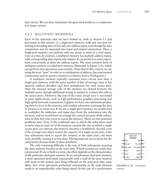
![230 C H A P T E R F I V E m e m o r i e s
dual-port memory, the effect of concurrent write operations depends on
when the operations are performed internally by the memory. We should
consult the data sheet for the memory component to understand the effect.
Some multiport memories, particularly those manufactured as pack-
aged components, provide additional circuits that compare the addresses on
the access ports and indicate when contention arises. They may also provide
circuits to arbitrate between conflicting accesses, ensuring that one proceeds
only after the other has completed. If we are using multiport memory compo-
nents or circuit blocks that do not provide such features and our application
may result in conflicting accesses, we need to include some form of arbitra-
tion as a separate part of the control section in our design. An alternative is
to ensure that the subsystems accessing the memory through separate ports
always access separate locations, for example, by ensuring that they always
operate on different blocks of data stored in different parts of the memory.
We will discuss block processing of data in more detail in Chapter 9.
example 5.7 Develop a Verilog model of a dual-port, 4K16-bit flow-
through SSRAM. One port allows data to be written and read, while the other
port only allows data to be read.
solution In the following module definition, the clk input is common to
both memory ports. The inputs and outputs with names ending in “1” are the
connections for the read/write memory port, and the inputs and outputs with
names ending in “2” are the connection for the read-only memory port.
module dual_port_SSRAM ( output reg [15:0] d_out1,
input [15:0] d_in1,
input [11:0] a1,
input en1, wr1,
output reg [15:0] d_out2,
input [11:0] a2,
input [11:0] en2,
input clk );
reg [15:0] data_RAM [0:4095];
always @(posedge clk) // read/write port
if (en1)
if (wr1) begin
data_RAM[a1] = d_in1; d_out1 = d_in1;
end
else
d_out1 = data_RAM[a1];
always @(posedge clk) // read-only port
if (en2) d_out2 = data_RAM[a2];
endmodule](https://image.slidesharecdn.com/digitaldesign-anembeddedsystemsapproachusingverilog-220525003453-7ebc98ea/85/Digital-Design-An-Embedded-Systems-Approach-Using-Verilog-pdf-251-320.jpg)
![236 C H A P T E R F I V E m e m o r i e s
solution The decoder has five input bits: four for the BCD code and one
for the blanking control. It has seven output bits: one for each segment. Thus,
we need a 327-bit ROM, as shown in Figure 5.21. The contents of the ROM
are given in Table 5.2.
example 5.10 Develop a Verilog model of the 7-segment decoder of
Example 5.9.
solution The module definition is
module seven_seg_decoder ( output reg [7:1] seg,
input [3:0] bcd,
input blank );
always @*
case ({blank, bcd})
5'b00000: seg = 7'b0111111; // 0
5'b00001: seg = 7'b0000110; // 1
5'b00010: seg = 7'b1011011; // 2
5'b00011: seg = 7'b1001111; // 3
5'b00100: seg = 7'b1100110; // 4
5'b00101: seg = 7'b1101101; // 5
5'b00110: seg = 7'b1111101; // 6
5'b00111: seg = 7'b0000111; // 7
5'b01000: seg = 7'b1111111; // 8
5'b01001: seg = 7'b1101111; // 9
5'b01010, 5'b01011,
5'b01100, 5'b01101,
5'b01110, 5'b01111:
seg = 7'b1000000; // – for invalid code
default: seg = 7'b0000000; // blank
endcase
endmodule
a ddr ess content address content
0 0111111 6 1111101
1 0000110 7 0000111
2 1011011 8 1111111
3 1001111 9 1101111
4 1100110 10–15 1000000
5 1101101 16–31 0000000
TAB LE 5.2 ROM contents for
the 7-segment decoder.
a
b
c
d
e
f
g
BCD0
BCD1
BCD2
BCD3
blank
A0
A1
A2
A3
A4
D0
D1
D2
D3
D4
D5
D6
FIG U R E 5.21 A 32×7-bit
ROM used as a 7-segment decoder.](https://image.slidesharecdn.com/digitaldesign-anembeddedsystemsapproachusingverilog-220525003453-7ebc98ea/85/Digital-Design-An-Embedded-Systems-Approach-Using-Verilog-pdf-257-320.jpg)
![As in Example 2.16, we use a case statement in a combinational always block
to implement a truth-table form of the mapping. In this example, however, we
form the address from the concatenation of the blank and bcd inputs. The case
statement then specifies the outputs for all possible combinations of value for the
address. A synthesis tool could then infer a ROM to implement the mapping.
In FPGA fabrics that provide SSRAM blocks, we can use an SSRAM
block as a ROM. We simply modify the always-block template for the
memory to omit the part that updates the memory content. We could
include a case statement to determine the data output, as in Example 5.10.
For example,
always @(posedge clk)
if (en)
case (a)
9'h0: d_out = 20'h00000;
9'h1: d_out = 20'h0126F;
...
endcase
The content of the memory is loaded into the FPGA as part of its
programming when the system is turned on. Thereafter, since the data
is not updated, it is constant. Note, in passing, that we have used the
Verilog notation for hexadecimal values in this model. The notation 9'h1
means a 9-bit vector zero-extended from the value 116, and the notation
20'h0126F means a 20-bit vector with the value 0126F16.
For large ROMs, writing the data directly in the Verilog code like this
is very cumbersome. Fortunately, Verilog provides a way of writing the
data in a separate file that can be loaded into the ROM during simula-
tion or synthesis. We use the $readmemh or $readmemb system task, as
follows:
reg [19:0] data_ROM [0:511];
...
initial $readmemh(rom.data, data_ROM);
always @posedge clk)
if (en)
d_out = data_ROM[a];
The $readmemh system task expects the content of the named file to be
a sequence of hexadecimal numbers, separated by spaces or line breaks.
Similarly, $readmemb expects the file to contain a sequence of binary
5.2 Memory Types C H A P T E R F I V E 237](https://image.slidesharecdn.com/digitaldesign-anembeddedsystemsapproachusingverilog-220525003453-7ebc98ea/85/Digital-Design-An-Embedded-Systems-Approach-Using-Verilog-pdf-258-320.jpg)


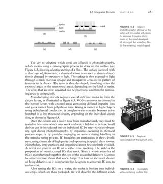
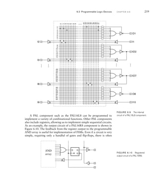
![and synchronous preset signals in common with other OLMCs in the
component. The select inputs of the multiplexers are set by programming
the component. The four-input multiplexer allows selection of registered
or combinational output, either inverting or noninverting. The two-input
multiplexer allows either registered or combinational feedback, or, if the
output driver is in the high-impedance state, direct input from the com-
ponent pin. By appropriate programming, a GAL component can emulate
any of the PAL components, including the PAL16L8 and PAL16R8 com-
ponents we have shown here.
In modern designs, we would typically use PLDs such as GAL com-
ponents for simple combinational glue logic, and for relatively simple
sequential circuits. As with PAL components, we would describe the
required functionality in terms of Boolean equations and use a CAD
tool to determine the programming for the component. The circuitry of
the original GAL families was based on similar technology to EPROMs,
allowing them to be programmed, erased using ultraviolet light, and sub-
sequently reprogrammed. Current components can be erased electrically
and programmed in situ in the final circuit.
example 6.2 Design a priority encoder that has 16 inputs, I[0:15]; a
four-bit encoded output, Z[3:0]; and a valid output that is 1 when any input is 1.
Input I[0] has the highest priority, and I[15] the lowest priority. The design is to be
implemented in a GAL22V10 component.
solution The Boolean equations for the encoder, expressed in Verilog, are
assign win[0] = I[0];
assign win[1] = I[1] ~I[0];
assign win[2] = I[2] ~I[1] ~I[0];
...
…
D
SP
AR
Q
Q
clk
0
1
2
3
0
1
FIGURE 6.12 Output
logic macrocell of a GAL22V10
component.
6.2 Programmable Logic Devices C H A P T E R S I X 261
(continued)](https://image.slidesharecdn.com/digitaldesign-anembeddedsystemsapproachusingverilog-220525003453-7ebc98ea/85/Digital-Design-An-Embedded-Systems-Approach-Using-Verilog-pdf-282-320.jpg)
![262 C H A P T E R S I X i m p l e m e n t a t i o n fa b r i c s
assign win[15] = I[15] ~I[14] ~I[13] ... ~I[0];
assign Z[3] = win[15] | win[14] | win[13] | win[12]
| win[11] | win[10] | win[9] | win[8];
assign Z[2] = win[15] | win[14] | win[13] | win[12]
| win[7] | win[6] | win[5] | win[4];
assign Z[1] = win[15] | win[14] | win[11] | win[10]
| win[7] | win[6] | win[3] | win[2];
assign Z[0] = win[15] | win[13] | win[11] | win[9]
| win[7] | win[5] | win[3] | win[1];
assign valid = I[15] | I[14] | I[13] | ... | I[0];
Each of the win elements can be implemented as a p-term in a row of the GAL
AND array. Each Z output is thus the OR of 8 p-terms. Since each OLMC in a
GAL22V10 component has at least 8 p-term inputs, these equations will fit in
any of the sections.
The valid output is the OR of 16 inputs, so it could fit in either of the two sec-
tions that have 16 p-term inputs to the OLMC. However, we can rewrite the
equation for valid using the DeMorgan law (see Section 2.1.2) as
assign valid ~(~I[15] ~I[14] ~I[13] ... ~I[0]);
By programming the OLMC for the valid output to negate the OR result, we can
use just one p-term. This allows us to place the valid output in any section of the
GAL component rather than only in those sections that have 16 OR-gate inputs.
The flexibility afforded by this transformation reduces the constraints on choice
of output pins for the component, and may thus simplify connection of the com-
ponent in a larger circuit.
6.2.2 C O M P L E X P L D S
A further evolution of PLDs, tracking advances in integrated circuit tech-
nology, led to the development of so-called complex programmable logic
devices (CPLDs). We can think of a CPLD as incorporating multiple PAL
structures, all interconnected by a programmable network of wires, as
shown in Figure 6.13. (This gives a general idea of CPLD organization.
The actual organization varies between components provided by different
manufacturers.) Each of the PAL structures consists of an AND array and
a number of embedded macrocells (M/Cs in the figure). The macrocells
contain OR gates, mutiplexers and flip-flops, allowing choice among
combinational or registered connections to other elements within the](https://image.slidesharecdn.com/digitaldesign-anembeddedsystemsapproachusingverilog-220525003453-7ebc98ea/85/Digital-Design-An-Embedded-Systems-Approach-Using-Verilog-pdf-283-320.jpg)
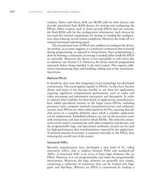
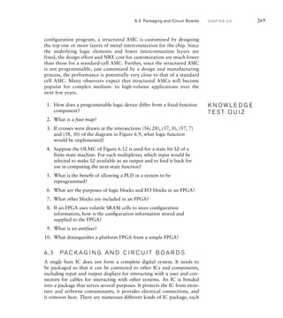
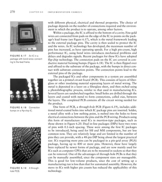
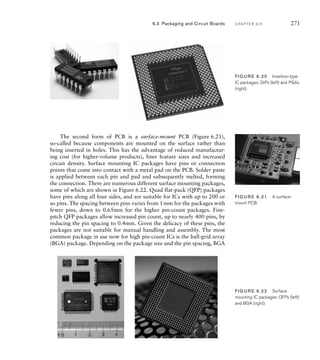
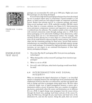
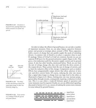
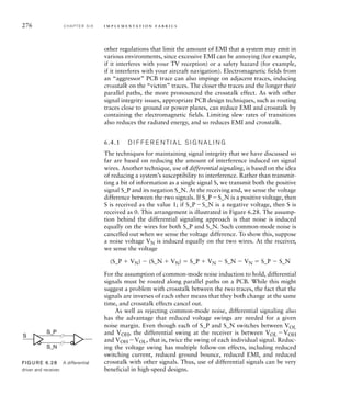


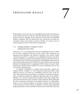
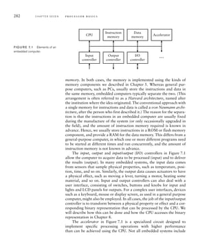

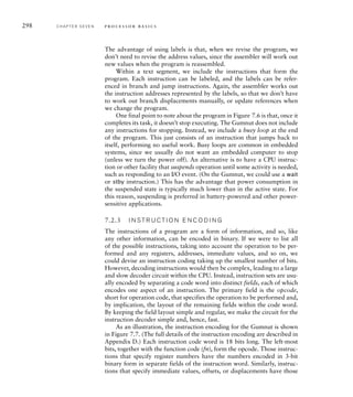
![302 C H A P T E R S E V E N p ro c e s s o r b a s i c s
7.3 I N T E R FA C I N G W I T H M E M O R Y
The way in which a CPU is connected to instruction and data memories
depends on the implementation fabric used for both the CPU and the
memories. In most embedded systems, the instruction memory is imple-
mented with ROM, NOR flash memory, SRAM, or a combination of
these. Including flash memory gives us the opportunity to upgrade the
embedded software in the field. The data memory is usually implemented
just with SRAM. Typically, the CPU and the memories each have a set of
connection signals for the CPU/memory interface, and it is our job to join
them together. If the two sets of signals are compatible, our job is rela-
tively easy. Often, however, the sets of signals are designed in isolation, or
according to different conventions. In such cases, we need to include glue
logic to complete the interface.
One of the simplest cases of interfacing a CPU with memory is that
of an embedded 8-bit core within an FPGA. The core includes interface
signals that connect directly to those of the FPGA’s memory blocks.
example 7.10 The memory interface signals of the Gumnut core are
described in the following Verilog module definition:
module gumnut ( input clk_i,
input rst_i,
output inst_cyc_o,
output inst_stb_o,
input inst_ack_i,
output [11:0] inst_adr_o,
input [17:0] inst_dat_i,
output data_cyc_o,
output data_stb_o,
output data_we_o,
input data_ack_i,
output [7:0] data_adr_o,
output [7:0] data_dat_o,
input [7:0] data_dat_i,
... );
endmodule
Show how to include an instance of the Gumnut core in a Verilog model of an
embedded system with a 2K 18-bit instruction memory and a 256 8-bit
data memory.
solution The ports in the module can interface with the control signals of
a flow-through SSRAM and a ROM implemented using FPGA SSRAM blocks,
as described in Sections 5.2.2 and 5.2.5. In our module for our embedded
system, we include the necessary nets and variables to connect to an instance](https://image.slidesharecdn.com/digitaldesign-anembeddedsystemsapproachusingverilog-220525003453-7ebc98ea/85/Digital-Design-An-Embedded-Systems-Approach-Using-Verilog-pdf-323-320.jpg)
![of the Gumnut entity, and use the nets and variables in always blocks for the
instruction and data memories. The module is
module embedded_gumnut;
reg [17:0] inst_ROM [0:2047];
reg [7:0] data_RAM [0:255];
wire clk;
wire rst;
wire inst_cyc_o;
wire inst_stb_o;
reg inst_ack_i;
wire [11:0] inst_adr_o;
reg [17:0] inst_dat_i;
wire data_cyc_o;
wire data_stb_o;
wire data_we_o;
reg data_ack_i;
wire [7:0] data_adr_o;
wire [7:0] data_dat_o;
reg [7:0] data_dat_i;
...
gumnut CPU ( .clk_i(clk_i), .rst_i(rst_i),
.inst_cyc_o(inst_cyc_o), .inst_stb_o(inst_stb_o),
.inst_ack_i(inst_ack_i),
.inst_adr_o(inst_adr_o), .inst_dat_i(inst_dat_i),
.data_cyc_o(data_cyc_o), .data_stb_o(data_stb_o),
.data_we_o(data_we_o), .data_ack_i(data_ack_i),
.data_adr_o(data_adr_o), .data_dat_o(data_dat_o),
.data_dat_i(data_dat_i), ... );
initial $readmemh(inst_ROM.data, inst_ROM);
always @(posedge clk) // Instruction memory
if (inst_cyc_o inst_stb_o) begin
inst_dat_i = inst_ROM[inst_adr_o[10:0]];
inst_ack_i = 1'b1;
end
else
inst_ack_i = 1'b0;
always @(posedge clk) // Data memory
if (data_cyc_o data_stb_o)
if (data_we_o) begin
data_RAM[data_adr_o] = data_dat_o;
data_dat_i = data_dat_o;
data_ack_i = 1'b1;
end
7.3 Interfacing with Memory C H A P T E R S E V E N 303
(continued)](https://image.slidesharecdn.com/digitaldesign-anembeddedsystemsapproachusingverilog-220525003453-7ebc98ea/85/Digital-Design-An-Embedded-Systems-Approach-Using-Verilog-pdf-324-320.jpg)
![304 C H A P T E R S E V E N p ro c e s s o r b a s i c s
else begin
data_dat_i = data_RAM[data_adr_o];
data_ack_i = 1'b1;
end
...
endmodule
Note that the instruction address port of the Gumnut core is 12 bits wide,
whereas the 2K 18-bit instruction memory uses an 11-bit-wide address. In this
design, we simply leave the most significant address bit of the core unconnected.
Each location in the instruction memory thus appears twice in the Gumnut’s
instruction address space: once at an address with the most significant bit 0, and
once at an address with the most significant bit 1. We would normally just use
one address for the location and ignore the other alias address.
Single-chip microcontrollers, such as those based on the 8051
described in Section 7.2.4, include a small amount of instruction and data
memory on the microcontroller chip. However, many of them are able to
address additional off-chip memory, using a number of the chip pins for
the external memory interface signals. Since using the pins for this purpose
reduces the number of pins available for inputs and outputs, the memory
interface pins are often multiplexed to perform different functions at dif-
ferent times. This complicates the connection between the microcontroller
and external memory.
As an illustration, we will describe how to expand the memory of the
8051 microcontroller. The 8051 can access up to 64K bytes of instruc-
tion memory and 64K bytes of data memory, however, there are only 256
bytes of data memory and 4K to 16K bytes of instruction memory on the
chip. The chip has two 8-bit input/output ports, P0 and P2, as well as a
number of control signals, that can be used to connect to external mem-
ory. Figure 7.8 shows how they would be used to connect to an external
128K 8-bit asynchronous SRAM, in which the lower 64K locations are
used for instructions and the upper 64K locations for data. P2 provides
the most significant address byte, and P0 is multiplexed with the least
significant address byte and instruction and data bytes. Since information
transfer on P0 is bidirectional, tristate drivers are used internally in the
microcontroller and in the memory data pins.
The 8051 activates the address-latch enable (ALE) signal when it
drives the least significant address bits on P0. We provide an 8-bit latch
to hold these bits for the remainder of the memory access cycle. During
an instruction read access, the 8051 activates the program-store enable
(
___
PSEN) signal, driving it to a low logic level. At other times, including data](https://image.slidesharecdn.com/digitaldesign-anembeddedsystemsapproachusingverilog-220525003453-7ebc98ea/85/Digital-Design-An-Embedded-Systems-Approach-Using-Verilog-pdf-325-320.jpg)
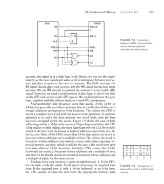
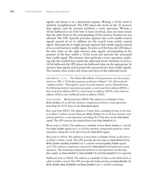
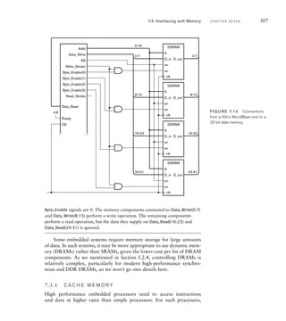
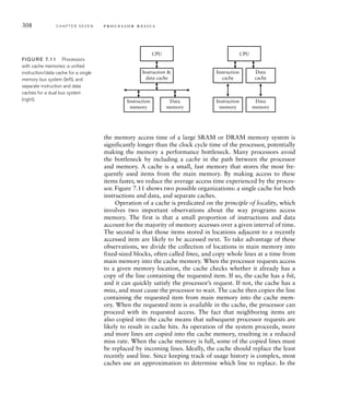


![324 C H A P T E R E I G H T i / o i n t e r fa c i n g
can achieve that rate by dividing the 10MHz clock down to 200Hz to activate
a 2-bit counter for selecting digits. A module to implement these design
decisions is
module display_mux ( output reg [3:0] anode_n,
output [7:0] segment_n,
input [3:0] bcd0, bcd1, bcd2, bcd3,
input clk, reset );
parameter clk_freq = 10000000;
parameter scan_clk_freq = 200;
parameter clk_divisor = clk_freq / scan_clk_freq;
reg scan_clk;
reg [1:0] digit_sel;
reg [3:0] bcd;
reg [7:0] segment;
integer count;
// Divide master clock to get scan clock
always @(posedge clk)
if (reset) begin
count = 0;
scan_clk = 1'b0;
end
else if (count == clk_divisor — 1) begin
count = 0;
scan_clk = 1'b1;
end
else begin
count = count + 1;
scan_clk = 1'b0;
end
// increment digit counter once per scan clock cycle
always @(posedge clk)
if (reset) digit_sel = 2'b00;
else if (scan_clk) digit_sel = digit_sel + 1;
// multiplexer to select a BCD digit
always @*
case (digit_sel)
2'b00: bcd = bcd0;
2'b01: bcd = bcd1;
2'b10: bcd = bcd2;
2'b11: bcd = bcd3;
endcase
(continued)](https://image.slidesharecdn.com/digitaldesign-anembeddedsystemsapproachusingverilog-220525003453-7ebc98ea/85/Digital-Design-An-Embedded-Systems-Approach-Using-Verilog-pdf-345-320.jpg)
![// activate selected digit's anode
always @*
case (digit_sel)
2'b00: anode_n = 4'b1110;
2'b01: anode_n = 4'b1101;
2'b10: anode_n = 4'b1011;
2'b11: anode_n = 4'b0111;
endcase
// 7-segment decoder for selected digit
always @*
case (bcd)
4'b0000: segment[6:0] = 7'b0111111; // 0
4'b0001: segment[6:0] = 7'b0000110; // 1
4'b0010: segment[6:0] = 7'b1011011; // 2
4'b0011: segment[6:0] = 7'b1001111; // 3
4'b0100: segment[6:0] = 7'b1100110; // 4
4'b0101: segment[6:0] = 7'b1101101; // 5
4'b0110: segment[6:0] = 7'b1111101; // 6
4'b0111: segment[6:0] = 7'b0000111; // 7
4'b1000: segment[6:0] = 7'b1111111; // 8
4'b1001: segment[6:0] = 7'b1101111; // 9
default: segment[6:0] = 7'b1000000; // -
endcase
// decimal point is only active for digit 3
always @* segment[7] = digit_sel == 2'b11;
// segment outputs are negative logic
assign segment_n = ~segment;
endmodule
The first always block is the clock divider that generates the 200Hz clock for
selecting digits. It sets the variable scan_clk to 1 for one master clock cycle at a
200Hz rate. The second always block implements the 2-bit counter, incrementing
the digit_sel variable each time scan_clk is 1. The next two always blocks use the
digit_sel signal to select the BCD digit and to activate the corresponding anode.
The remaining always block and assignments decode the selected digit to drive
the segment cathodes.
As an alternative to using LEDs for displays, some systems use liquid
crystal displays (LCDs). Each segment of an LCD consists of liquid crystal
material between two optical polarizing filters. The liquid crystal also
polarizes light, and, depending on the angle of polarization, can allow
light to pass or be blocked by the filters. The liquid crystal is forced to
twist or untwist, thus changing its axis of polarization, by application of
a voltage to electrodes in front of and behind the segment. By varying the
8.1 I/O Devices C H A P T E R E I G H T 325](https://image.slidesharecdn.com/digitaldesign-anembeddedsystemsapproachusingverilog-220525003453-7ebc98ea/85/Digital-Design-An-Embedded-Systems-Approach-Using-Verilog-pdf-346-320.jpg)
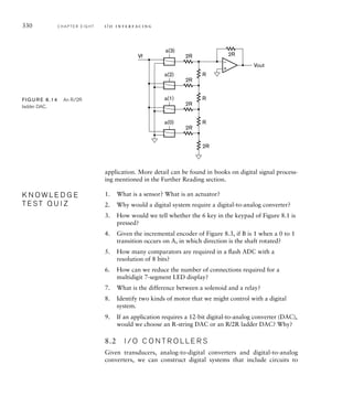
![332 C H A P T E R E I G H T i / o i n t e r fa c i n g
example 8.3 The signals provided by the Gumnut core for connecting to
I/O registers are described in the following Verilog module definition:
module gumnut ( input clk_i,
input rst_i,
...
output port_cyc_o,
output port_stb_o,
output port_we_o,
input port_ack_i,
output [7:0] port_adr_o,
output [7:0] port_dat_o,
input [7:0] port_dat_i,
... );
endmodule
The output port_adr_o is the port address, port_dat_o is the data written by an
out instruction, port_dat_i is the data read by an inp instruction, port_cyc_o
and port_stb_o indicate that a port read or write operation is to be performed,
port_we_o indicates that the operation is a write, and port_ack_i indicates that
the selected port is ready and has acknowledged completion of the read or write
operation.
Develop a controller for the keypad matrix shown in Figure 8.2, and show how
to connect the controller to a Gumnut core. Use output port address 4 for the
matrix row output register and input port address 4 for the matrix column input
register.
solution The controller connects to the Gumnut I/O signals on one
side and to the keypad row and column signals on the other side, as shown in
Figure 8.15. We decode the port address from the Gumnut core externally to the
controller to derive the strobe control signal (stb_i) for the controller.
port_dat_i
port_ack_i
port_adr_o
port_we_o
port_cyc_o
Gumnut
port_dat_o
port_stb_o stb_i
dat_i
cyc_i
we_i
Keypad Controller
dat_o
keypad_row
keypad_col
ack_o
=
keypad_port_
addr
1 2 3
4 5 6
7 8 9
* 0 #
FIG U R E 8.15 Connection
of a Gumnut core to a keypad
controller.](https://image.slidesharecdn.com/digitaldesign-anembeddedsystemsapproachusingverilog-220525003453-7ebc98ea/85/Digital-Design-An-Embedded-Systems-Approach-Using-Verilog-pdf-353-320.jpg)
![The Verilog module definition for the controller is
module keypad_controller ( input clk_i,
input cyc_i,
input stb_i,
input we_i,
output ack_o,
input [7:0] dat_i,
output reg [7:0] dat_o,
output reg [3:0] keypad_row,
input [2:0] keypad_col );
reg [2:0] col_synch;
always @(posedge clk_i) // Row register
if (cyc_i stb_i we_i) keypad_row = dat_i[3:0];
always @(posedge clk_i) begin // Column synchronizer
dat_o = {5'b0, col_synch};
col_synch = keypad_col;
end
assign ack_o = cyc_i stb_i;
endmodule
The first always block represents the keypad row output register, storing the
value to drive on the keypad row outputs. The second always block represents
the keypad column input register. Since the key switches may change at any time,
we need to synchronize the input with the clock to avoid metastability failures.
(We discussed this issue in Section 4.4.1.) In this design, we assume the keypad
controller is the only thing driving the port_dat_o outputs, so we can assign
directly to them regardless of the state of the control inputs. We will return to
the topic of connecting multiple controllers in Section 8.3. The final assignment
in the architecture body activates the port_ack_o output immediately on any port
read or write operation, since there is no need to make the processor wait.
The controller is connected to a Gumnut core in an embedded system as shown
in the following module outline:
module embedded_system;
wire ...
parameter [7:0] keypad_port_addr = 8'h04;
8.2 I/O Controllers C H A P T E R E I G H T 333
(continued)](https://image.slidesharecdn.com/digitaldesign-anembeddedsystemsapproachusingverilog-220525003453-7ebc98ea/85/Digital-Design-An-Embedded-Systems-Approach-Using-Verilog-pdf-354-320.jpg)
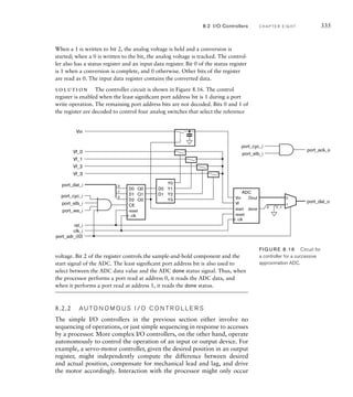
![example 8.6 Develop a Verilog model for the embedded system of
Example 8.5.
solution The module definition is
module embedded_system_ADC_keypad;
wire ...
parameter [7:0] ADC0_port_addr = 8'h00,
ADC1_port_addr = 8'h02,
keypad_port_addr = 8'h04;
wire ADC0_stb_o, ADC1_stb_o, keypad_stb_o;
wire [7:0] ADC0_dat_o, ADC1_dat_o, keypad_dat_o,
ADC0_dat_fwd, ADC1_dat_fwd;
wire ADC0_ack_o, ADC1_ack_o, keypad_ack_o,
ADC0_ack_fwd, ADC1_ack_fwd;
gumnut processor_core
( .clk_i(clk), .rst_i(rst), ...,
.port_cyc_o(port_cyc_o), .port_stb_o(port_stb_o),
.port_we_o(port_we_o), .port_ack_i(ADC1_ack_fwd),
.port_adr_o(port_adr_o), .port_dat_o(port_dat_o),
.port_dat_i(ADC1_dat_fwd), ... );
assign ADC0_stb_o = (port_adr_o 8'hFE)
== ADC0_port_addr port_stb_o;
assign ADC1_stb_o = (port_adr_o 8'hFE)
== ADC1_port_addr port_stb_o;
assign keypad_stb_o = port_adr_o
== keypad_port_addr port_stb_o;
keypad_controller keypad ( .clk_i(clk),
.cyc_i(port_cyc_o),
.stb_i(keypad_stb_o),
.we_i(port_we_o),
.ack_o(keypad_ack_o),
.dat_i(port_dat_o),
.dat_o(keypad_dat_o), ... );
ADC_controller ADC0 ( .clk_i(clk), .rst_i(rst),
.cyc_i(port_cyc_o), .stb_i(ADC0_stb_o),
.we_i(port_we_o), .ack_o(ADC0_ack_o),
.adr_i(port_adr_o[0]), .dat_i(port_dat_o),
.dat_o(ADC0_dat_o), ... );
assign ADC0_dat_fwd = ADC0_stb_o ? ADC0_dat_o : keypad_dat_o;
assign ADC0_ack_fwd = ADC0_stb_o ? ADC0_ack_o : keypad_ack_o;
(continued)
8.3 Parallel Buses C H A P T E R E I G H T 341](https://image.slidesharecdn.com/digitaldesign-anembeddedsystemsapproachusingverilog-220525003453-7ebc98ea/85/Digital-Design-An-Embedded-Systems-Approach-Using-Verilog-pdf-362-320.jpg)
![342 C H A P T E R E I G H T i / o i n t e r fa c i n g
ADC_controller ADC1 ( .clk_i(clk), .rst_i(rst),
.cyc_i(port_cyc_o), .stb_i(ADC1_stb_o),
.we_i(port_we_o), .ack_o(ADC1_ack_o),
.adr_i(port_adr_o[0]), .dat_i(port_dat_o),
.dat_o(ADC1_dat_o), ... );
assign ADC1_dat_fwd = ADC1_stb_o ? ADC1_dat_o : ADC0_dat_fwd;
assign ADC1_ack_fwd = ADC1_stb_o ? ADC1_ack_o : ADC0_ack_fwd;
endmodule
The first group of assignments, after the Gumnut core instance, represent the
port address decoders. They compare the port address from the processor core
with the base addresses of the ADC controllers and the keypad controllers. For
the ADC controllers, the port address is ANDed with the hexadecimal value FE
to clear the least significant bit.
The instances of the ADC controllers are followed by assignments that represent
the distributed multiplexers. The outputs of the multiplexers for the second ADC
connect back to the Gumnut core port_dat_i and port_ack_i inputs.
8.3.2 T R I S TAT E B U S E S
A second solution to avoiding contention on a bus is to use tristate bus
drivers. We introduced tristate drivers in Chapter 5 as part of our discussion
of connecting multiple memory components. We said that the outputs of a
tristate driver can be turned off by placing it in a high-impedance, or hi-Z,
state. The symbol for a tristate driver is shown in Figure 8.22. When the
enable input is 1, the driver behaves like an ordinary output, driving either a
low or a high logic level on the output. When the enable input is 0, the driver
enters the high-impedance state by turning its output-stage transistors off.
We can implement a bus with multiple data sources by using tristate
drivers on the outputs of each data source. We use one driver for each bit
of encoded data provided by the source, and connect the enable inputs of
the drivers for a given source together, as shown in Figure 8.23. That way,
a source either drives a data value onto the bus, or has all bits in the high-
impedance state. The control section selects a particular source to provide
data by setting the enable input of that source’s drivers to 1, and all other
enable inputs to 0.
One of the main advantages of tristate buses is the reduction in wiring
that they afford. For each bit of the encoded data on the bus, one signal
wire is connected between all of the data sources and destinations. How-
ever, there are some issues to consider. First, since bus wires connect all of
the sources and destinations, they are generally long and heavily loaded
bus(0)
d(0)
en
…
…
…
bus(1)
d(1)
bus(2)
d(2)
bus(n)
d(n)
FIG U R E 8.23 Parallel
connection of tristate drivers.
output
input
enable
FIG U R E 8.22 Symbol for a
tristate driver.](https://image.slidesharecdn.com/digitaldesign-anembeddedsystemsapproachusingverilog-220525003453-7ebc98ea/85/Digital-Design-An-Embedded-Systems-Approach-Using-Verilog-pdf-363-320.jpg)
![346 C H A P T E R E I G H T i / o i n t e r fa c i n g
For multibit buses, we can use vectors whose elements include
Z values. While we can assign 0, 1 and Z values individually to elements
of vectors, we usually assign either a vector containing just 0 and 1 values
to represent an enabled driver or a vector of all Z values to represent a
disabled driver. Verilog’s implicit resizing rules for vector values involve
extending with Z elements if the leftmost bit of the value to be extended is
Z. So we can write 8'bz to get an 8-element vector of Z values.
example 8.8 The SN74x16541 component manufactured by Texas
Instruments is a dual 8-bit bus buffer/driver in a package for use in a printed cir-
cuit board system. The internal circuit of the component is shown in Figure 8.27.
Develop a Verilog model of the component.
solution We can use vector ports for each of the 8-bit inputs and out-
puts, and single-bit ports for the enable inputs. The module definition is:
module sn74x16541 ( output tri [7:0] y1, y2,
input [7:0] a1, a2,
input en1_1, en1_2, en2_1, en2_2 );
assign y1 = (~en1_1 ~en1_2) ? a1 : 8'bz;
assign y2 = (~en2_1 ~en2_2) ? a2 : 8'bz;
endmodule
Each assignment within the module represents one of the 8-bit sections of the
component. The condition in the assignment determines whether the 8-bit
tristate driver is enabled or disabled. The driver is disabled by assigning a vector
value consisting of all Z elements. Note the use of the tri keyword in the declara-
tion of the output ports to indicate that they can be assigned Z values.
When we have multiple data sources for a tristate bus, our Verilog
model includes multiple assignment statements that assign values to the
bus. Verilog must resolve the values contributed by the separate assign-
ments to determine the final value for the bus. If one assignment con-
tributes 0 or 1 to a bus and all of the others contribute Z, the 0 or 1
value overrides the others and becomes the bus value. This corresponds
to the normal case of one driver being enabled and the rest disabled.
If one assignment contributes 0 and another contributes 1, we have a
conflict. Verilog then uses the special value X, called unknown, as the
final bus value, since it is unknown whether a real circuit would pro-
duce a low, high or invalid logic level on the bus. Depending on how the
Verilog model of a data destination receiving an X value is written, it
might propagate the unknown value to its outputs, or produce arbitrary
y1(0)
a1(0)
a1(1)
…
…
…
a1(7)
en1_1
en1_2
y1(1)
y1(7)
y2(0)
a2(0)
a2(1)
…
…
…
a2(7)
en2_1
en2_2
y2(1)
y2(7)
FIG U R E 8.27 Internal circuit
of the 16541 component.](https://image.slidesharecdn.com/digitaldesign-anembeddedsystemsapproachusingverilog-220525003453-7ebc98ea/85/Digital-Design-An-Embedded-Systems-Approach-Using-Verilog-pdf-367-320.jpg)
![0 or 1 values. Ideally, it would include a verification test statement that
would detect unknown input values. If all assignments to a bus contribute
Z, the final signal value is Z. This corresponds to the bus floating. Again,
since this does not represent a valid logic level, a Verilog model of a data
destination receiving a Z input should propagate an X output and detect
the error condition.
An important point to realize about the Z and X values is that they do
not represent real logic levels in a physical circuit. Rather, assignment of
Z to an output is a notational device interpreted by synthesis CAD tools
as implying a tristate driver for the output. Assignment of X to an output
is a notational device used in simulation to propagate error conditions in
cases where we cannot determine a valid output value. We can write Ver-
ilog statements that test whether a bus has the value Z or X, but it only
makes sense to do so in testbench models, for example, in an if statement
to verify that all drivers of a bus have been disabled or that there is no bus
conflict. Since, according to our digital abstraction, signals in a physical
circuit are only ever 0 or 1, a real digital component cannot sense any
other level.
If we need to test for Z or X values in a testbench model, we should
use different equality and inequality operators from those we have used
so far. The == operator in Verilog, known as the logical equality operator,
represents a hardware equivalence operation. If either operand is Z or X,
the result is X, since it is unknown whether the values in a real circuit are
equivalent or not. Similarly, the != operator, logical inequality, represents
a hardware unequivalence operation, and returns X if either operand is Z
or X. Thus, for example, the expressions 1'b0 == 1'bX and 1'bZ != 1'b1
both yield X. If we want to test for Z and X values, we must use the
=== and !== operators, known as the case equality and case inequality
operators, respectively. These perform an exact comparison, including X
and Z values. Thus, 1'b0 === 1'bX yields 0 (false), and 1'bZ !=== 1'b1
yields 1 (true). Note that, like the Z value, we can use an uppercase or
lowercase letter, and we can only write literal X values in binary, octal, or
hexadecimal numbers.
example 8.9 Suppose a Verilog module includes the following
declarations and assignments
tri [11:0] data_1, data_2, data_bus;
wire sel_1, sel_2;
...
assign data_bus = sel_1 ? data_1 : 12'hz;
assign data_bus = sel_2 ? data_2 : 12'hz;
8.3 Parallel Buses C H A P T E R E I G H T 347](https://image.slidesharecdn.com/digitaldesign-anembeddedsystemsapproachusingverilog-220525003453-7ebc98ea/85/Digital-Design-An-Embedded-Systems-Approach-Using-Verilog-pdf-368-320.jpg)


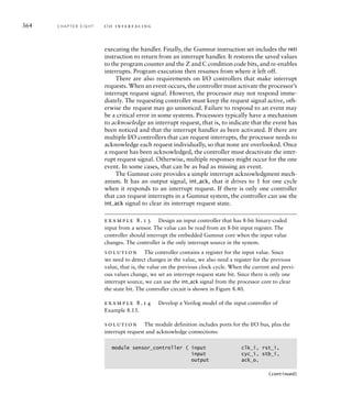
![D
reset
Q D
reset
Q
D
reset
Q
≠
dat_o
int_req
ack_o
clk_i
rst_i
int_ack
cyc_i
stb_i
sensor_in
clk clk
clk
FIG U R E 8.40 Circuit for
an input controller with interrupt
request logic.
8.5 I/O Software C H A P T E R E I G H T 365
output reg [7:0] dat_o,
output reg int_req,
input int_ack,
input [7:0] sensor_in );
reg [7:0] prev_data;
always @(posedge clk_i) // Data registers
if (rst_i) begin
prev_data = 8'b0;
dat_o = 8'b0;
end
else begin
prev_data = dat_o;
dat_o = sensor_in;
end
always @(posedge clk_i) // Interrupt state
if (rst_i) int_req = 1'b0;
else
case (int_req)
1'b0: if (dat_o != prev_data) int_req = 1'b1;
1'b1: if (int_ack) int_req = 1'b0;
endcase
assign ack_o = cyc_i stb_i;
endmodule
The first always block represents the two data registers, one for the current sen-
sor data value and one for the previous value. The second always block repre-
sents the interrupt request and acknowledge logic. It is essentially a small finite
state machine, with int_req encoding the state. In the state where int_req is 0,
there is no interrupt request. However, if the current value changes from the pre-
vious value, int_req is set to 1. The value of this output is used as the interrupt
request signal to the processor. It stays 1, even when the current value and the
previous value no longer differ. Eventually, when the processor responds to the
interrupt and sets int_ack to 1, int_req is cleared back to 0.](https://image.slidesharecdn.com/digitaldesign-anembeddedsystemsapproachusingverilog-220525003453-7ebc98ea/85/Digital-Design-An-Embedded-Systems-Approach-Using-Verilog-pdf-386-320.jpg)
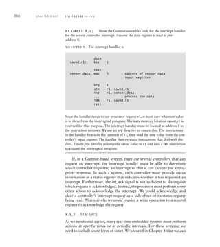
![use a counter to derive a periodic signal from the system clock. We can
use such a signal as a time base: each cycle represents one unit of time in
the embedded system. We also showed how we can use a loadable down
counter as an interval timer. A common use for interval timers in real-time
embedded systems is to generate an interrupt for the processor at some
programmable multiple of a time base. The interval timer acts as an I/O
controller, often called a real-time clock, with an output register for pro-
gramming the time interval. The interrupt handler for the timer can then
perform any required periodic actions.
example 8.16 Develop a Verilog model for a real-time clock controller
for the Gumnut processor. The controller has a 10µs time base derived from
a 50MHz system clock, and an 8-bit output register for the value to load into
the counter. A write operation to the output register causes the counter to be
loaded. After the counter reaches 0, it reloads the value from the output register
and requests an interrupt. The controller has an input register for reading the
current count value. The counter also has a 1-bit control output register. When
bit 0 of the register is 0, interrupts from the controller are masked, and when it
is 1, they are enabled. The counter has a status register, in which bit 0 is 1 when
the counter has reached 0 and been reloaded, or 0 otherwise. Other bits of the
register are read as 0. Reading the register has the side effect of acknowledging a
requested interrupt and clearing bit 0. The counter output and input registers are
located at the base port address, and the control and status registers are at offset
1 from the base port address.
solution The module definition for the controller has ports for the I/O
bus, and uses the stb_i port for the decoded base port address:
module real_time_clock ( input clk_i, // 50MHz clock
input rst_i,
input cyc_i, stb_i, we_i,
output ack_o,
input adr_i,
input [7:0] dat_i,
output [7:0] dat_o,
output int_req );
parameter clk_freq = 50000000;
parameter timebase_freq = 100000;
parameter timebase_divisor = clk_freq / timebase_freq;
reg [7:0] count_value;
reg trigger_interrupt;
reg int_enabled, int_triggered;
8.5 I/O Software C H A P T E R E I G H T 367
(continued)](https://image.slidesharecdn.com/digitaldesign-anembeddedsystemsapproachusingverilog-220525003453-7ebc98ea/85/Digital-Design-An-Embedded-Systems-Approach-Using-Verilog-pdf-388-320.jpg)
![368 C H A P T E R E I G H T i / o i n t e r fa c i n g
integer timebase_count;
reg [7:0] count_start_value;
always @(posedge clk_i) // Counter
if (rst_i) begin
timebase_count = 0;
count_start_value = 8'b0;
count_value = 8'b0;
trigger_interrupt = 1'b0;
end
else if (cyc_i stb_i !adr_i we_i) begin
timebase_count = 0;
count_start_value = dat_i;
count_value = dat_i;
trigger_interrupt = 1'b0;
end
else if (timebase_count == timebase_divisor – 1) begin
timebase_count = 0;
if (count_value == 8'b00000000) begin
count_value = count_start_value;
trigger_interrupt = 1'b1;
end else begin
count_value = count_value — 1;
trigger_interrupt = 1'b0;
end
end
else begin
timebase_count = timebase_count + 1;
trigger_interrupt = 1'b0;
end
always @(posedge clk_i) // Control register
if (rst_i)
int_enabled = 1'b0;
else if (cyc_i stb_i adr_i we_i)
int_enabled = dat_i[0];
always @(posedge clk_i) // Interrupt register
if (rst_i || (cyc_i stb_i adr_i !we_i))
int_triggered = 1'b0;
else if (trigger_interrupt)
int_triggered = 1'b1;
assign dat_o = !adr_i ? count_value : {7'b0, int_triggered};
assign int_req = int_triggered int_enabled;
assign ack_o = cyc_i stb_i;
endmodule](https://image.slidesharecdn.com/digitaldesign-anembeddedsystemsapproachusingverilog-220525003453-7ebc98ea/85/Digital-Design-An-Embedded-Systems-Approach-Using-Verilog-pdf-389-320.jpg)
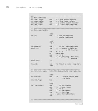


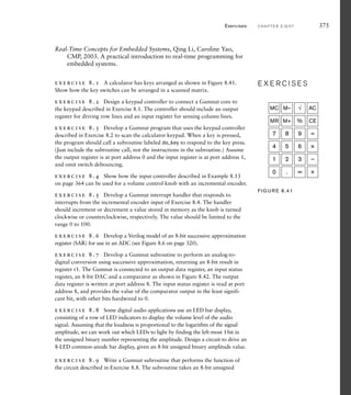
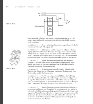
![This approximation works, because the square-root and square functions
are both monotonic (that is, they increase as the operand increases and
decrease as the operand decreases). Hence, the maxima and minima in
the true magnitude and the approximate magnitude occur at the same
places in the image. Computing the approximation involves much less
hardware than computing the square and square-root functions. We
repeat the computation of the approximate magnitude for each pixel
position in the image. Note that the pixels around the edge of the image
do not have a complete set of neighboring pixels, so we need to treat
them separately. The simplest approach is to set the value of D for
the edge pixels of the derivative image to 0. Since that is a relatively
straightforward process and is not time consuming, we can implement
it in software.
example 9.2 Express the Sobel edge-detection algorithm more formally
in a pseudo-code notation, that is, a notation like a computer programming
language.
solution We will use a pseudo-code notation like Verilog. Let O[row] [col]
denote pixels in the original image, and D[row] [col] denote pixels in the deriva-
tive image, where row ranges from 0 to 479 and col ranges from 0 to 639. Also,
let Gx[i] [j] and Gy[i] [j] denote the convolution masks, where i and j range from
–1 to 1. The algorithm is
for (row = 1; row = 478; row = row + 1) begin
for (col = 1; col = 638; col = col + 1) begin
sumx = 0; sumy = 0;
for (i = –1; i = +1; i = i + 1) begin
for (j = –1; j = +1; j = j + 1) begin
sumx = sumx + 0[row+i][col+j] * Gx[i][j];
sumy = sumy + 0[row+i][col+j] * Gy[i][j];
end
end
D[row][col] = abs(sumx) + abs(sumy)
end
end
example 9.3 Calculate the number of bits required to represent interme-
diate and final values for pixels in the Sobel convolution.
solution Each pixel is represented as an 8-bit unsigned number. Given
the coefficient values in the convolution masks, the partial products range from
–510 to 510. Thus, the partial products should be represented using 10-bit
signed numbers. There are nine partial products to add to form each of Dx and
9.2 Case Study: Video Edge-Detection C H A P T E R N I N E 387](https://image.slidesharecdn.com/digitaldesign-anembeddedsystemsapproachusingverilog-220525003453-7ebc98ea/85/Digital-Design-An-Embedded-Systems-Approach-Using-Verilog-pdf-411-320.jpg)
![However, this group of four pixel values is what we should write to the
beginning of the derivative image row. As we mentioned earlier, the left-
most position does not have a complete set of neighbors, so we don’t
compute a value for it. We will rely on the embedded software to clear
that pixel value to 0 subsequently.
When we reach the end of a row, we need to drain the pipeline. Since
the number of pixels in a row is a multiple of four (6401604), we can
always read complete groups of four pixels each. After reading the last
group, we perform four computation cycles normally. This gives us four
result pixels to write, plus three remaining pixel values in the pipeline.
We finish the row by writing the four result pixels, omitting the reads,
performing four further computation cycles to drain the pipeline and shift
the last pixel values into the required positions in the result register, and
performing a final write. Note that this places an invalid value in the
right-most result pixel register. This corresponds to the right-most pixel
of a row, which does not have a complete set of neighbors. Again, we will
rely on the embedded software to clear that pixel value to 0.
example 9.7 Develop Verilog RTL code to describe the datapath of
Figure 9.6.
solution The code in the module definition for the Sobel accelerator is
// Computation datapath signals
reg [31:0] prev_row, curr_row, next_row;
reg [7:0] O [-1:+1][-1:+1];
reg signed [10:0] Dx, Dy, D;
reg [7:0] abs_D;
reg [31:0] result_row;
...
// Computational datapath
always @(posedge clk_i) // Previous row register
if (prev_row_load) prev_row = dat_i;
else if (shift_en) prev_row[31:8] = prev_row[23:0];
always @(posedge clk_i) // Current row register
if (curr_row_load) curr_row = dat_i;
else if (shift_en) curr_row[31:8] = curr_row[23:0];
always @(posedge clk_i) // Next row register
if (next_row_load) next_row = dat_i;
(continued)
9.2 Case Study: Video Edge-Detection C H A P T E R N I N E 393](https://image.slidesharecdn.com/digitaldesign-anembeddedsystemsapproachusingverilog-220525003453-7ebc98ea/85/Digital-Design-An-Embedded-Systems-Approach-Using-Verilog-pdf-417-320.jpg)
![394 C H A P T E R N I N E a c c e l e r a t o rs
else if (shift_en) next_row[31:8] = next_row[23:0];
function [10:0] abs (input signed [10:0] x);
abs = x = 0 ? x : –x;
endfunction
always @(posedge clk_i) // Computation pipeline
if (shift_en) begin
D = abs(Dx) + abs(Dy);
abs_D = D[10:3];
Dx = – $signed({3'b000, 0[–1][–1]}) // – 1 * 0[-1][-1]
+ $signed({3'b000, 0[-1][+1]}) // + 1 * 0[-1][+1]
– ($signed({3'b000, 0[ 0][-1]}) // – 2 * 0[ 0][-1]
1)
+ ($signed({3'b000, 0[ 0][+1]}) // + 2 * 0[ 0][+1]
1)
– $signed({3'b000, 0[+1][-1]}) // – 1 * 0[+1][-1]
+ $signed({3'b000, 0[+1][+1]}); // + 1 * 0[+1][+1]
Dy = $signed({3'b000, 0[-1][-1]}) // + 1 * O[-1][-1]
+ ($signed({3'b000, 0[-1][ 0]}) // + 2 * 0[-1][ 0]
1)
+ $signed({3'b000, 0[-1][+1]}) // + 1 * 0[-1][+1]
– $signed({3'b000, 0[+1][-1]}) // – 1 * 0[+1][-1]
– ($signed({3'b000, 0[+1][ 0]}) // – 2 * 0[+1][ 0]
1)
– $signed({3'b000, 0[+1][+1]}); // – 1 * 0[+1][+1]
0[-1][-1] = 0[-1][0];
0[-1][ 0] = 0[-1][+1];
0[-1][+1] = prev_row[31:24];
O[ 0][-1] = O[0][0];
O[ 0][ 0] = O[0][+1];
O[ 0][+1] = curr_row[31:24];
O[+1][-1] = O[+1][ 0];
O[+1][ 0] = O[+1][+1];
O[+1][+1] = next_row[31:24];
end
always @(posedge clk_i) // Result row register
if (shift_en) result_row = {result_row[23:0], abs_D};
The first three always blocks in the module represent the three registers into
which groups of four pixels are read from memory. Each block has a separate
control signal governing loading, since the registers are loaded in successive
memory read operations. They share a control signal for shifting, since they all
shift a pixel out into the pipeline in parallel.
The next always block, as the comment suggests, represents the computational
pipeline of the accelerator. The signals to which the block assigns, governed by](https://image.slidesharecdn.com/digitaldesign-anembeddedsystemsapproachusingverilog-220525003453-7ebc98ea/85/Digital-Design-An-Embedded-Systems-Approach-Using-Verilog-pdf-418-320.jpg)
![the shift_en control signal, represent the pipeline registers. The signal O is a
33 array of pixel values, with indices corresponding to the difference in row
and column numbers from those of the derivative pixel computed from the reg-
ister values. For example, the element with indices [1][1] contains the pixel
in the previous row and next column from the pixel being computed. Values
are shifted into this array leftward from the left-most 8 bits of each of the input
registers. The Dx and Dy values are computed from the array element values. In
each case, the values are resized to 11 bits and converted to signed numbers, as
we discussed earlier in our analysis of the precision requirements for the com-
putation. Multiplying by 2 is performed with a logical shift left by one position,
and multiplying by a negative coefficient is implemented by subtraction instead
of addition. The absolute values of the Dx and Dy values, implemented by the
abs function defined in the module, are added, and then scaled back from 11 to
8 bits to yield the final derivative pixel value.
The remaining always block represents the register that accumulates groups of
four derivative pixels for writing to memory. Pixels are shifted into this register
under control of the shift_en signal.
We mentioned earlier that a block-processing accelerator needs cir-
cuits for address generation, as well as for processing the data. Our Sobel
accelerator needs circuits to compute the addresses for reading pixels
from the original image and for writing pixels to the derivative image. We
will provide a register into which the embedded software can write the
base addresses for the original image and the derivative image in memory.
The address generator needs to determine pixel addresses using the base
addresses. We will require that all addresses are word aligned, that is,
that they are all multiples of four. This means the two least significant
address bits are always 00, and so do not need to be computed or explic-
itly stored.
example 9.8 Given a base address B for an image in memory, derive
equations for computing the address of a pixel in row r and column c of the
image. Rows and columns are numbered from 0.
solution The image size is 480 rows of 640 pixels per row. The starting
address of row r is
Br640
The pixel in column c in that row is then located at address
Br640c
We can treat the expression r640c as an address offset from the base address.
9.2 Case Study: Video Edge-Detection C H A P T E R N I N E 395](https://image.slidesharecdn.com/digitaldesign-anembeddedsystemsapproachusingverilog-220525003453-7ebc98ea/85/Digital-Design-An-Embedded-Systems-Approach-Using-Verilog-pdf-419-320.jpg)
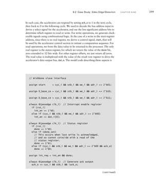
![// Address generator
always @(posedge clk_i) // 0 base address register
if (0_base_ce) 0_base = dat_i[21:2];
always @(posedge clk_i) // 0 address offset counter
if (offset_reset) 0_offset = 0;
else if (0_offset_cnt_en) 0_offset = 0_offset + 1;
assign 0_prev_addr = 0_base + 0_offset;
assign 0_curr_addr = 0_prev_addr + 640/4;
assign 0_next_addr = 0_prev_addr + 1280/4;
always @(posedge clk_i) // D base address register
if (D_base_ce) D_base = dat_i[21:2];
always @(posedge clk_i) // D address offset counter
if (offset_reset) D_offset = 0;
else if (D_offset_cnt_en) D_offset = D_offset + 1;
assign D_addr = D_base + D_offset;
assign adr_o[21:2] = prev_row_load ? 0_prev_addr :
curr_row_load ? 0_curr_addr :
next_row_load ? 0_next_addr :
D_addr;
assign adr_o[1:0] = 2'b00;
The always blocks commented as being base address registers represent the
base address registers for the original and derivative images, respectively. The
always blocks commented as being address offset counters represent the counters
for pixel groups read and written, respectively. The registers and counters are
governed by control signals generated by the accelerator’s control section. The
adders are represented by the combinational assignments to the four address
signals O_prev_addr, O_curr_addr, O_next_addr and D_addr. The assignment to
the bus address signal adr_o represents the multiplexer that chooses among the
generated addresses for memory read and write operations.
The remaining aspect of the Sobel accelerator design is control
sequencing. We have touched on the sequence needed for computation of
the derivative image, row-by-row and pixel-group at a time. This includes
sequencing of write and read operations with the accelerator as a bus
master. We also need to sequence the accelerator’s response as a bus slave
9.2 Case Study: Video Edge-Detection C H A P T E R N I N E 397](https://image.slidesharecdn.com/digitaldesign-anembeddedsystemsapproachusingverilog-220525003453-7ebc98ea/85/Digital-Design-An-Embedded-Systems-Approach-Using-Verilog-pdf-421-320.jpg)
![In each case, the accelerator can respond by setting ack_o to 1 in the next cycle,
then back to 0 in the following cycle. We need to decode the bus address input to
derive a select signal for the accelerator, and use the less significant address bits to
determine which register to read or write. For write operations, we generate clock-
enable signals using combinational logic. In the case of a write to the start-register
address, since there is no real register, we derive a control signal, start, that will
be used by the accelerator control section to initiate a computation sequence. For
read operations, we form the data value to be returned to the processor. The only
real register is the status register, for which we return the value of the done bit,
zero extended to 32 bits wide. For other register offsets, we just return all zeros.
The read value is multiplexed with the value of the result row register to drive the
accelerator’s data output bus, dat_o. The model code describing these aspects is
// Wishbone slave interface
assign start = cyc_i stb_i we_i adr_i == 2'b01;
assign 0_base_ce = cyc_i stb_i we_i adr_i == 2'b10;
assign D_base_ce = cyc_i stb_i we_i adr_i == 2'b11;
always @(posedge clk_i) // Interrupt enable register
if (rst_i)
int_en = 1'b0;
else if (cyc_i stb_i we_i adr_i == 2'b00)
int_en = dat_i[0];
always @(posedge clk_i) // Status register
if (rst_i)
done = 1'b0;
else if (done_set)
// This occurs when last write is acknowledged,
// and so cannot coincide with a read of the
// status register.
done = 1'b1;
else if (cyc_i stb_i we_i adr_i == 2'b00 ack_o)
done = 1'b0;
assign int_req = int_en done;
always @(posedge clk_i) // Generate ack output
ack_o = cyc_i stb_i !ack_o;
(continued)
9.2 Case Study: Video Edge-Detection C H A P T E R N I N E 399](https://image.slidesharecdn.com/digitaldesign-anembeddedsystemsapproachusingverilog-220525003453-7ebc98ea/85/Digital-Design-An-Embedded-Systems-Approach-Using-Verilog-pdf-423-320.jpg)
![idle
write_result read_prev read_curr read_next
comp1 comp2 comp3 comp4
start = 1
ack = 1 ack = 1
ack = 1
ack = 1 ack = 1 ack = 1
ack = 1
ack = 1
read_prev_0 read_curr_0 read_next_0
comp1_0 comp2_0 comp3_0 comp4_0
write_158 comp1_159 comp2_159 comp3_159 comp4_159
write_159
col = 158
col /= 158
ack = 1 and row /= 477
ack = 1 and row = 477
FIG U R E 9.10 State
transition diagram for the Sobel
accelerator control section.
9.2 Case Study: Video Edge-Detection C H A P T E R N I N E 401
in Table 9.2. Other control signals are Mealy outputs. For these, in Table 9.3,
we have shown the input conditions that, along with the current state, determine
their values. As in the state transition diagram, we have omitted the complemen-
tary conditions. In those cases, the Mealy outputs remain 0.
example 9.13 Develop Verilog model code for the control section.
solution The control-section code includes declarations of internal signals
for the control FSM, the row and column counters, and the control signals:
parameter [4:0] idle = 5'b00000,
read_prev_0 = 5'b00001,
read_curr_0 = 5'b00010,
read_next_0 = 5'b00011,
comp1_0 = 5'b00100,
(continued)](https://image.slidesharecdn.com/digitaldesign-anembeddedsystemsapproachusingverilog-220525003453-7ebc98ea/85/Digital-Design-An-Embedded-Systems-Approach-Using-Verilog-pdf-425-320.jpg)
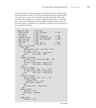
![404 C H A P T E R N I N E a c c e l e r a t o rs
comp2_0 = 5'b00101,
comp3_0 = 5'b00110,
comp4_0 = 5'b00111,
read_prev = 5'b01000,
read_curr = 5'b01001,
read_next = 5'b01010,
comp1 = 5'b01011,
comp2 = 5'b01100,
comp3 = 5'b01101,
comp4 = 5'b01110,
write_result = 5'b01111,
write_158 = 5'b10000,
comp1_159 = 5'b10001,
comp2_159 = 5'b10010,
comp3_159 = 5'b10011,
comp4_159 = 5'b10100,
write_159 = 5'b10101;
reg [4:0] current_state, next_state;
reg [9:0] row; // range 0 to 477;
reg [7:0] col; // range 0 to 159;
wire 0_base_ce, D_base_ce;
wire start;
reg offset_reset, row_reset, col_reset;
reg prev_row_load, curr_row_load, next_row_load;
reg shift_en;
reg row_cnt_en, col_cnt_en;
reg 0_offset_cnt_en, D_offset_cnt_en;
reg int_en, done_set, done;
The two counters used by the control section to keep track of progress through
rows and columns, respectively, are represented by the following always blocks:
always @(posedge clk_i) // Row counter
if (row_reset) row = 0;
else if (row_cnt_en) row = row + 1;
always @(posedge clk_i) // Column counter
if (col_reset) col = 0;
else if (col_cnt_en) col = col + 1;
Next, the model includes blocks representing the finite-state machine using the
techniques we have described in previous chapters. The state register is repre-
sented by the block:
always @(posedge clk_i) // State register
if (rst_i) current_state = idle;
else current_state = next_state;](https://image.slidesharecdn.com/digitaldesign-anembeddedsystemsapproachusingverilog-220525003453-7ebc98ea/85/Digital-Design-An-Embedded-Systems-Approach-Using-Verilog-pdf-428-320.jpg)
![solution Our testbench is modeled after the general system organization
shown in Figure 9.2. The accelerator is the design under verification, and the
arbiter and bus functional processor and memory form the remainder of the test-
bench. We also include a clock and reset generator. The outline of the testbench
module definition is
`timescale 1ns/1ns
module testbench;
parameter t_c = 10;
parameter [22:0] mem_base = 23'h000000;
parameter [22:0] saobel_reg_base = 23'h400000;
parameter sobel_int_reg_offset = 0;
parameter sobel_start_reg_offset = 4;
parameter sobel_O_base_reg_offset = 8;
parameter sobel_D_base_reg_offset = 12;
parameter sobel_status_reg_offset = 0;
reg clk, rst;
wire bus_cyc, bus_stb, bus_we;
wire [3:0] bus_sel;
wire [22:0] bus_adr;
wire bus_ack;
wire [31:0] bus_dat;
wire int_req;
wire sobel_cyc_o, sobel_stb_o, sobel_we_o;
wire [21:0] sobel_adr_o;
wire sobel_ack_i;
wire sobel_stb_i;
wire sobel_ack_o;
wire [31:0] sobel_dat_o;
...
always begin // Clock generator
clk = 1'b1; #(t_c/2);
clk = 1'b0; #(t_c/2);
end
initial begin // Reset generator
rst = 1'b1;
#(2.5*t_c) rst = 1'b0;
end
sobel duv ( .clk_i(clk), .rst_i(rst),
.cyc_o(sobel_cyc_o), .stb_o(sobel_stb_o),
(continued)
9.3 Verifying an Accelerator C H A P T E R N I N E 409](https://image.slidesharecdn.com/digitaldesign-anembeddedsystemsapproachusingverilog-220525003453-7ebc98ea/85/Digital-Design-An-Embedded-Systems-Approach-Using-Verilog-pdf-433-320.jpg)
![410 C H A P T E R N I N E a c c e l e r a t o rs
.we_o(sobel_we_o),
.adr_o(sobel_adr_o), .ack_i(sobel_ack_i),
.cyc_i(bus_cyc), .stb_i(sobel_stb_i),
.we_i(bus_we), .adr_i(bus_adr[3:2]),
.ack_o(sobel_ack_o),
.dat_o(sobel_dat_o), .dat_i(bus_dat),
.int_req(int_req) );
...
endmodule
The clock generator always block uses the parameter t_c for the clock cycle time,
giving a clock frequency of 100MHz. The parameters mem_base and sobel_base
define the base addresses of the memory (00000016) and the Sobel accelerator
registers (40000016). Additional parameters define the offsets from the base
address for the control and status registers. Next, the testbench includes nets
for the bus address, data and control signals. As we will see shortly, these are
multiplexed from the various sources in the system. The testbench also declares
nets for connection specifically to the Sobel accelerator. Within the module, the
accelerator is instantiated as the design under verification (duv) and connected to
the nets.
The testbench code for the processor bus functional model is
reg cpu_cyc_o, cpu_stb_o, cpu_we_o;
reg [3:0] cpu_sel_o;
reg [22:0] cpu_adr_o;
wire cpu_ack_i;
reg [31:0] cpu_dat_o;
wire[31:0] cpu_dat_i;
...
task bus_write ( input [22:0] adr, input [31:0] dat );
begin
cpu_adr_o = adr;
cpu_sel_o = 4'b1111;
cpu_dat_o = dat;
cpu_cyc_o = 1'b1; cpu_stb_o = 1'b1; cpu_we_o = 1'b1;
@(posedge clk); while (!cpu_ack_i) @(posedge clk);
end
endtask
...
initial begin // Processor bus-functional model
cpu_adr_o = 23'h000000;
cpu_sel_o = 4'b0000;
(continued)](https://image.slidesharecdn.com/digitaldesign-anembeddedsystemsapproachusingverilog-220525003453-7ebc98ea/85/Digital-Design-An-Embedded-Systems-Approach-Using-Verilog-pdf-434-320.jpg)
![cpu_dat_o = 32'h00000000;
cpu_cyc_o = 1'b0; cpu_stb_o = 1'b0; cpu_we_o = 1'b0;
@(negedge rst);
@(posedge clk);
// Write 008000 (hex) to 0_base_addr register
bus_write(sobel_reg_base
+ sobel_0_base_reg_offset, 32'h00008000);
// Write 053000 + 280 (hex) to D_base_addr register
bus_write(sobel_reg_base
+ sobel_D_base_reg_offset, 32'h00053280);
// Write 1 to interrupt control register (enable interrupt)
bus_write(sobel_reg_base
+ sobel_int_reg_offset, 32'h00000001);
// Write to start register (data value ignored)
bus_write(sobel_reg_base
+ sobel_start_reg_offset, 32'h00000000);
// End of write operations
cpu_cyc_o = 1'b0; cpu_stb_o = 1'b0; cpu_we_o = 1'b0;
begin: loop
forever begin
#10000;
@(posedge clk);
// Read status register
cpu_adr_o = sobel_reg_base + sobel_status_reg_offset;
cpu_sel_o = 4'b1111;
cpu_cyc_o = 1'b1; cpu_stb_o = 1'b1; cpu_we_o = 1'b0;
@(posedge clk); while (!cpu_ack_i) @(posedge clk);
cpu_cyc_o = 1'b0; cpu_stb_o = 1’b0; cpu_we_o = 1'b0;
if (cpu_dat_i[0]) disable loop;
end
end
end
The processor waits for completion of system reset, then performs the required
sequence of bus write operations to initialize the accelerator. For each bus
operation, described by the bus_write task, the processor assigns the appropri-
ate values to the address, data and control signals, then waits for the accelera-
tor to acknowledge completion of the operation. After completion of the write
to the start register, the processor enters a loop in which it waits for 10µs,
resynchronizes with the clock, then reads the accelerator status register. When
the accelerator acknowledges completion of the read operation, the processor
checks whether the done bit is 1. If so, the processor exits the loop, completing
the test.
9.3 Verifying an Accelerator C H A P T E R N I N E 411](https://image.slidesharecdn.com/digitaldesign-anembeddedsystemsapproachusingverilog-220525003453-7ebc98ea/85/Digital-Design-An-Embedded-Systems-Approach-Using-Verilog-pdf-435-320.jpg)
![412 C H A P T E R N I N E a c c e l e r a t o rs
The testbench code for the memory bus functional model is
wire mem_stb_i;
wire [3:0] mem_sel_i;
reg mem_ack_o;
reg [31:0] mem_dat_o;
...
always begin // Memory bus-functional model
mem_ack_o = 1'b0;
mem_dat_o = 32'h00000000;
@(posedge clk);
while (!(bus_cyc mem_stb_i)) @(posedge clk);
if (!bus_we)
mem_dat_o = 32'h00000000; // in place of read data
mem_ack_o = 1'b1;
@(posedge clk);
end
The memory repeatedly waits until the bus_cyc and mem_stb_i signals are both
1, indicating that a memory operation is required. If bus_we is 0, the operation
is a read, so the memory provides zeros on the data outputs. In the case of a
write operation, the memory does nothing with the input data. In either case, the
memory sets the acknowledge signal to 1, and then on the next clock cycle clears
the signal back to 0, completing the operation.
The arbiter for the testbench is somewhat more involved than the other
testbench components. It uses the sobel_cyc_o and cpu_cyc_o signals as
requests from the Sobel accelerator and the processor, respectively, and
generates sobel_gnt and cpu_gnt grant signals. When either of the request
signals is activated, the arbiter activates the corresponding grant. If both
requests are activated in the same cycle, the arbiter gives preference to the
accelerator, activating its grant and leaving the processor’s grant inactive until
the accelerator’s request is deactivated. Since the grant outputs depend not only
on the values of the request inputs, but also on the preceding history of request
values, the arbiter must be implemented as a sequential circuit using an FSM.
The state transition diagram is shown in Figure 9.11. The FSM is a Mealy
machine, since that allows us to activate a grant signal in the same cycle in
which the corresponding request is activated.
The testbench code for the arbiter is
parameter sobel = 1'b0, cpu = 1'b1;
reg arbiter_current_state, arbiter_next_state;
(continued)](https://image.slidesharecdn.com/digitaldesign-anembeddedsystemsapproachusingverilog-220525003453-7ebc98ea/85/Digital-Design-An-Embedded-Systems-Approach-Using-Verilog-pdf-436-320.jpg)
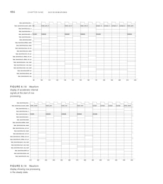
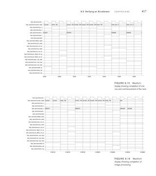


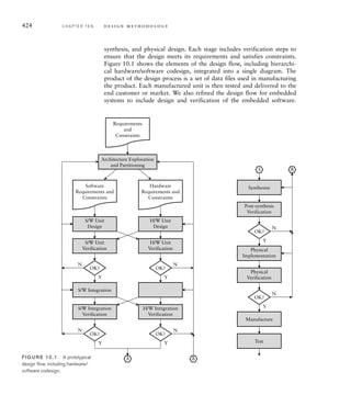
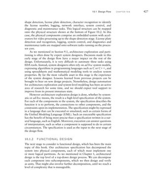
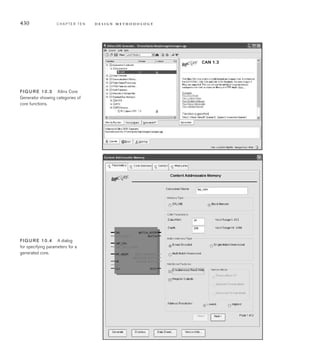
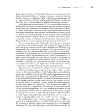

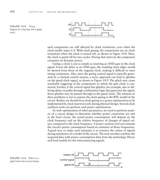

![448 C H A P T E R T E N d e s i g n m e t h o d o l o g y
We can test whether the synthesis tool treats arithmetic expressions in this way by
rewriting the statements in the pipeline always block of the Verilog code as follows:
Dx = ( – $signed({3'b000, O[ –1][–1]}) // – 1 * O[–1][–1]
+ $signed({3'b000, O[ –1][+1]}) // + 1 * O[-1][+1]
– ($signed({3'b000, O[ 0][-1]}) // – 2 * O[ 0][–1]
1) )
+ ( ($signed({3'b000, O[ 0][+1]}) // + 2 * O[ 0][+1]
1)
– $signed({3'b000, O[+1][–1]}) // – 1 * O[+1][–1]
+ $signed({3'b000, O[+1][+1]}) ); // + 1 * O[+1][+1]
Dy = ( $signed({3’b000, O[–1][–1]}) // + 1 * O[-1][–1]
+ ($signed({3'b000, O[-1][ 0]}) // + 2 * O[-1][ 0]
1)
+ $signed({3'b000, O[-1][+1]}) ) // + 1 * O[-1][+1]
– ( $signed({3'b000, O[+1][–1]}) // – 1 * O[+1][–1]
+ ($signed({3'b000, O[+1][ 0]}) // – 2 * O[+1][ 0]
1)
+ $signed({3'b000, O[+1][+1]}) ); // – 1 * O[+1][+1]
With this change in place, and using maximum optimization options for the synthesis
and PAR tools, we reduce the synthesis estimate of the clock period to 9.515ns and
the post-PAR estimate to 9.864ns. This just satisfies our timing constraint, with a
1.4% margin. In practice, we would prefer to have a larger margin, and so might try
further revision of the model code to reduce the path delay. If regrouping the arith-
metic expression shown above is insufficient, we might be able to move part of the
computation to the paths after the Dx and Dy registers, where there is more slack.
10.2.3 P O W E R O P T I M I Z AT I O N
As digital systems have become more complex, power consumption has
become a more significant constraint in their design. This is particularly
the case for mobile battery-operated devices, such as cell phones, PDAs,
and portable media players. The amount of power consumed by the circuit
directly affects how long the device functions on a single battery charge,
or, alternatively, how large a battery is required. Even in fixed mains-
powered systems, power consumption is important. Electrical power con-
sumed by a circuit is turned into heat, which must be dissipated through
the chip and system packaging. Dealing with additional heat dissipation
adds cost to a system, so keeping power consumption to a minimum is
part of keeping cost down.
As we mentioned in Section 10.2.1, many of the approaches to mini-
mizing circuit area also help reduce power consumption, since larger cir-
cuits generally contain more transistors, each of which consumes power.
However, there are other approaches we can consider that focus on power
consumption. One such approach is to identify blocks of a system that](https://image.slidesharecdn.com/digitaldesign-anembeddedsystemsapproachusingverilog-220525003453-7ebc98ea/85/Digital-Design-An-Embedded-Systems-Approach-Using-Verilog-pdf-475-320.jpg)
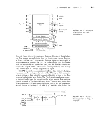
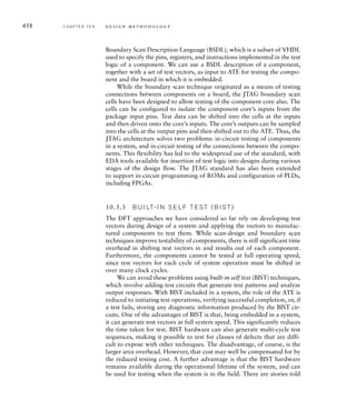
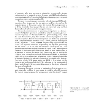
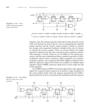


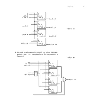


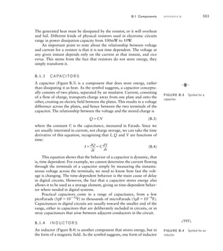
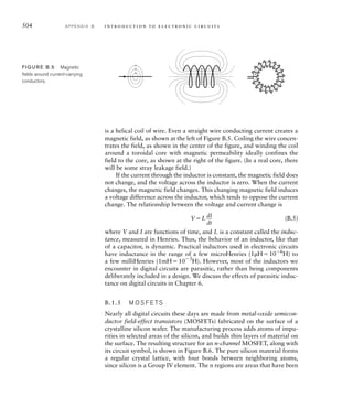
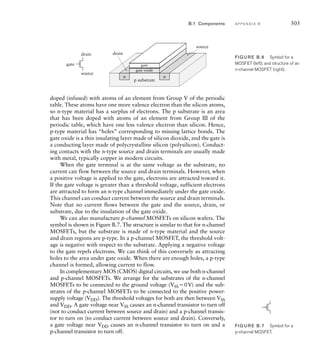
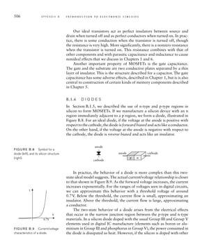
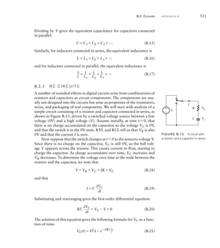
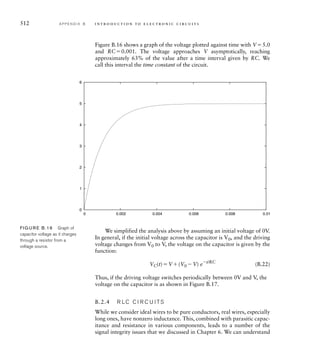
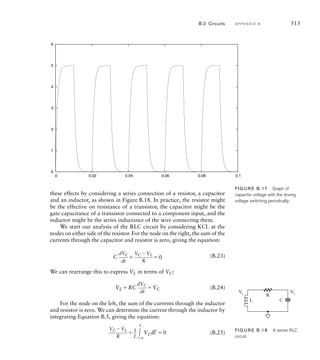
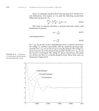

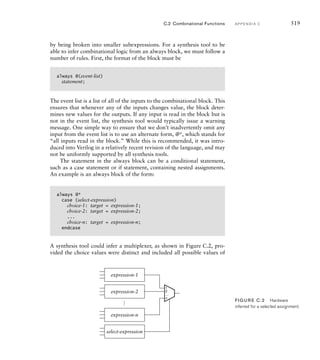
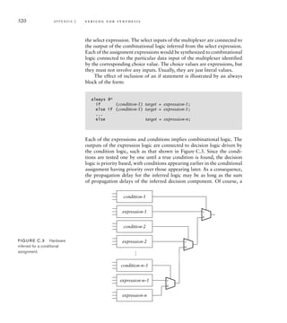
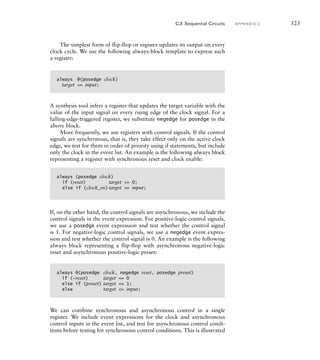
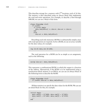
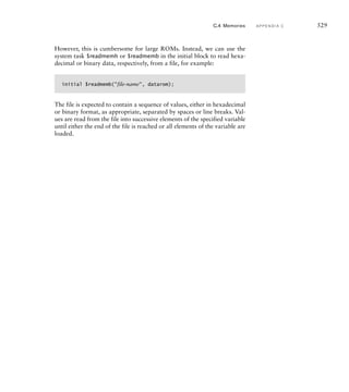

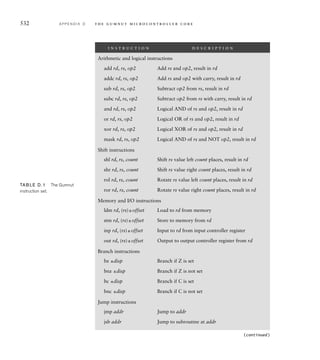
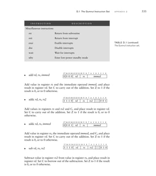
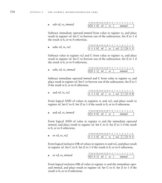
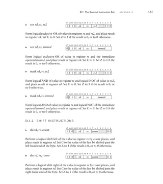
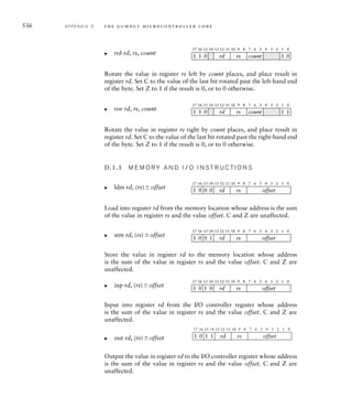
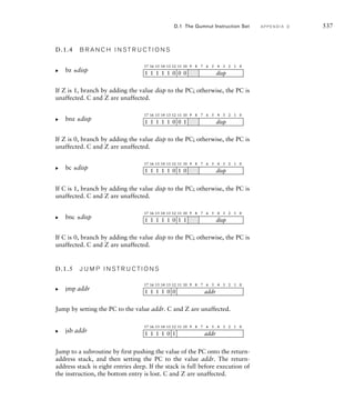
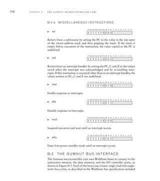
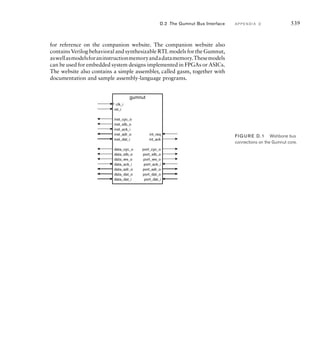

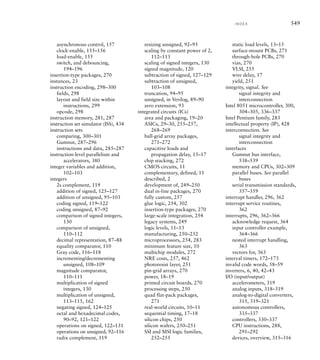
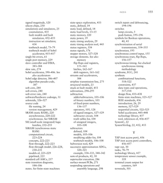


![ECE 2103_L6 Boolean Algebra Canonical Forms [Autosaved].pptx](https://cdn.slidesharecdn.com/ss_thumbnails/ece2103l6booleanalgebracanonicalformsautosaved-240213191859-861c7560-thumbnail.jpg?width=640&height=640&fit=bounds)