2. ACS30MS
Die Characteristics
DIE DIMENSIONS: PASSIVATION:
Size: 2390µm x 2390µm (94 mils x 94 mils) Type: Phosphorous Silicon Glass (PSG)
Thickness: 525µm ±25µm (20.6 mils ±1 mil) Thickness: 1.30µm ±0.15µm
Bond Pad: 110µm x 110µm (4.3 x 4.3 mils)
SPECIAL INSTRUCTIONS
METALLIZATION: AI Bond VCC First
Metal 1 Thickness: 0.7µm ±0.1µm
ADDITIONAL INFORMATION:
Metal 2 Thickness: 1.0µm ±0.1µm
Worst Case Current Density: <2.0 x 10⁵ A/cm2
SUBSTRATE POTENTIAL Transistor Count: 86
Unbiased Insulator
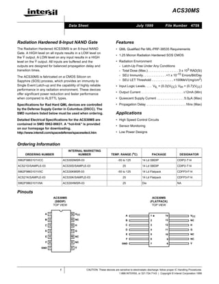
Metallization Mask Layout
ACS30MS
B A VCC
(2) (1) (14) NC
C (3) (12) H
D (4) (11) G
NC NC
E (5) NC
(6) (7) (8) NC
F GND Y
All Intersil semiconductor products are manufactured, assembled and tested under ISO9000 quality systems certification.
Intersil semiconductor products are sold by description only. Intersil Corporation reserves the right to make changes in circuit design and/or specifications at any time with-
out notice. Accordingly, the reader is cautioned to verify that data sheets are current before placing orders. Information furnished by Intersil is believed to be accurate and
reliable. However, no responsibility is assumed by Intersil or its subsidiaries for its use; nor for any infringements of patents or other rights of third parties which may result
from its use. No license is granted by implication or otherwise under any patent or patent rights of Intersil or its subsidiaries.
For information regarding Intersil Corporation and its products, see web site www.intersil.com
Sales Office Headquarters
NORTH AMERICA EUROPE ASIA
Intersil Corporation Intersil SA Intersil (Taiwan) Ltd.
P. O. Box 883, Mail Stop 53-204 Mercure Center 7F-6, No. 101 Fu Hsing North Road
Melbourne, FL 32902 100, Rue de la Fusee Taipei, Taiwan
TEL: (321) 724-7000 1130 Brussels, Belgium Republic of China
FAX: (321) 724-7240 TEL: (32) 2.724.2111 TEL: (886) 2 2716 9310
FAX: (32) 2.724.22.05 FAX: (886) 2 2715 3029
2