Downloaded 79 times

![VLSI Physical Design: From Graph Partitioning to Timing Closure Chapter 5: Global Routing
©KLMH
Lienig
©2011SpringerVerlag
40
[1]
N [2] 8,6
W [4] 1,4
W [4] 1,4
parent of node [node name] ∑w1(s,node),∑w2(s,node)
Group 2 Group 31 4 7
2 5 8
3 6 9
1,4 8,8
2,6 2,8
9,8 3,3
8,6 9,7 3,2
1,4 2,8 4,5
Current node: 1
Neighboring nodes: 2, 4
Minimum cost in group 2: node 4
s
t](https://image.slidesharecdn.com/cadglobalrouting-140705013857-phpapp02/75/Computer-Aided-Design-Global-Routing-40-2048.jpg)
![VLSI Physical Design: From Graph Partitioning to Timing Closure Chapter 5: Global Routing
©KLMH
Lienig
©2011SpringerVerlag
41
1 4 7
2 5 8
3 6 9
1,4 8,8
2,6 2,8
9,8 3,3
8,6 9,7 3,2
1,4 2,8 4,5
Group 2 Group 3
[1]
N [2] 8,6
W [4] 1,4
W [4] 1,4
N [5] 10,11
W [7] 9,12
N [2] 8,6
Current node: 4
Neighboring nodes: 1, 5, 7
Minimum cost in group 2: node 2
s
t
parent of node [node name] ∑w1(s,node),∑w2(s,node)](https://image.slidesharecdn.com/cadglobalrouting-140705013857-phpapp02/75/Computer-Aided-Design-Global-Routing-41-2048.jpg)
![VLSI Physical Design: From Graph Partitioning to Timing Closure Chapter 5: Global Routing
©KLMH
Lienig
©2011SpringerVerlag
42
1 4 7
2 5 8
3 6 9
1,4 8,8
2,6 2,8
9,8 3,3
8,6 9,7 3,2
1,4 2,8 4,5
Group 2 Group 3
[1]
N [2] 8,6
W [4] 1,4
W [4] 1,4
N [5] 10,11
W [7] 9,12
N [2] 8,6
N [3] 9,10
W [5] 10,12
N [3] 9,10
Current node: 2
Neighboring nodes: 1, 3, 5
Minimum cost in group 2: node 3
s
t
parent of node [node name] ∑w1(s,node),∑w2(s,node)](https://image.slidesharecdn.com/cadglobalrouting-140705013857-phpapp02/75/Computer-Aided-Design-Global-Routing-42-2048.jpg)
![VLSI Physical Design: From Graph Partitioning to Timing Closure Chapter 5: Global Routing
©KLMH
Lienig
©2011SpringerVerlag
43
1 4 7
2 5 8
3 6 9
1,4 8,8
2,6 2,8
9,8 3,3
8,6 9,7 3,2
1,4 2,8 4,5
Group 2 Group 3
[1]
N [2] 8,6
W [4] 1,4
W [4] 1,4
N [5] 10,11
W [7] 9,12
N [2] 8,6
N [3] 9,10
W [5] 10,12
N [3] 9,10W [6] 18,18
N [5] 10,11Current node: 3
Neighboring nodes: 2, 6
Minimum cost in group 2: node 5
s
t
parent of node [node name] ∑w1(s,node),∑w2(s,node)](https://image.slidesharecdn.com/cadglobalrouting-140705013857-phpapp02/75/Computer-Aided-Design-Global-Routing-43-2048.jpg)
![VLSI Physical Design: From Graph Partitioning to Timing Closure Chapter 5: Global Routing
©KLMH
Lienig
©2011SpringerVerlag
44
1 4 7
2 5 8
3 6 9
1,4 8,8
2,6 2,8
9,8 3,3
8,6 9,7 3,2
1,4 2,8 4,5
Group 2 Group 3
[1]
N [2] 8,6
W [4] 1,4
W [4] 1,4
N [5] 10,11
W [7] 9,12
N [2] 8,6
N [3] 9,10
W [5] 10,12
N [3] 9,10W [6] 18,18
N [5] 10,11
N [6] 12,19
W [8] 12,19
W [7] 9,12
Current node: 5
Neighboring nodes: 2, 4, 6, 8
Minimum cost in group 2: node 7
s
t
parent of node [node name] ∑w1(s,node),∑w2(s,node)](https://image.slidesharecdn.com/cadglobalrouting-140705013857-phpapp02/75/Computer-Aided-Design-Global-Routing-44-2048.jpg)
![VLSI Physical Design: From Graph Partitioning to Timing Closure Chapter 5: Global Routing
©KLMH
Lienig
©2011SpringerVerlag
45
1 4 7
2 5 8
3 6 9
1,4 8,8
2,6 2,8
9,8 3,3
8,6 9,7 3,2
1,4 2,8 4,5
Group 2 Group 3
(1)
N (2) 8,6
W (4) 1,4
W (4) 1,4
N (5) 10,11
W (7) 9,12
N (2) 8,6
N (3) 9,10
W (5) 10,12
N (3) 9,10W (6) 18,18
N (5) 10,11
N (6) 12,19
W (8) 12,19
W (7) 9,12N (8) 12,14
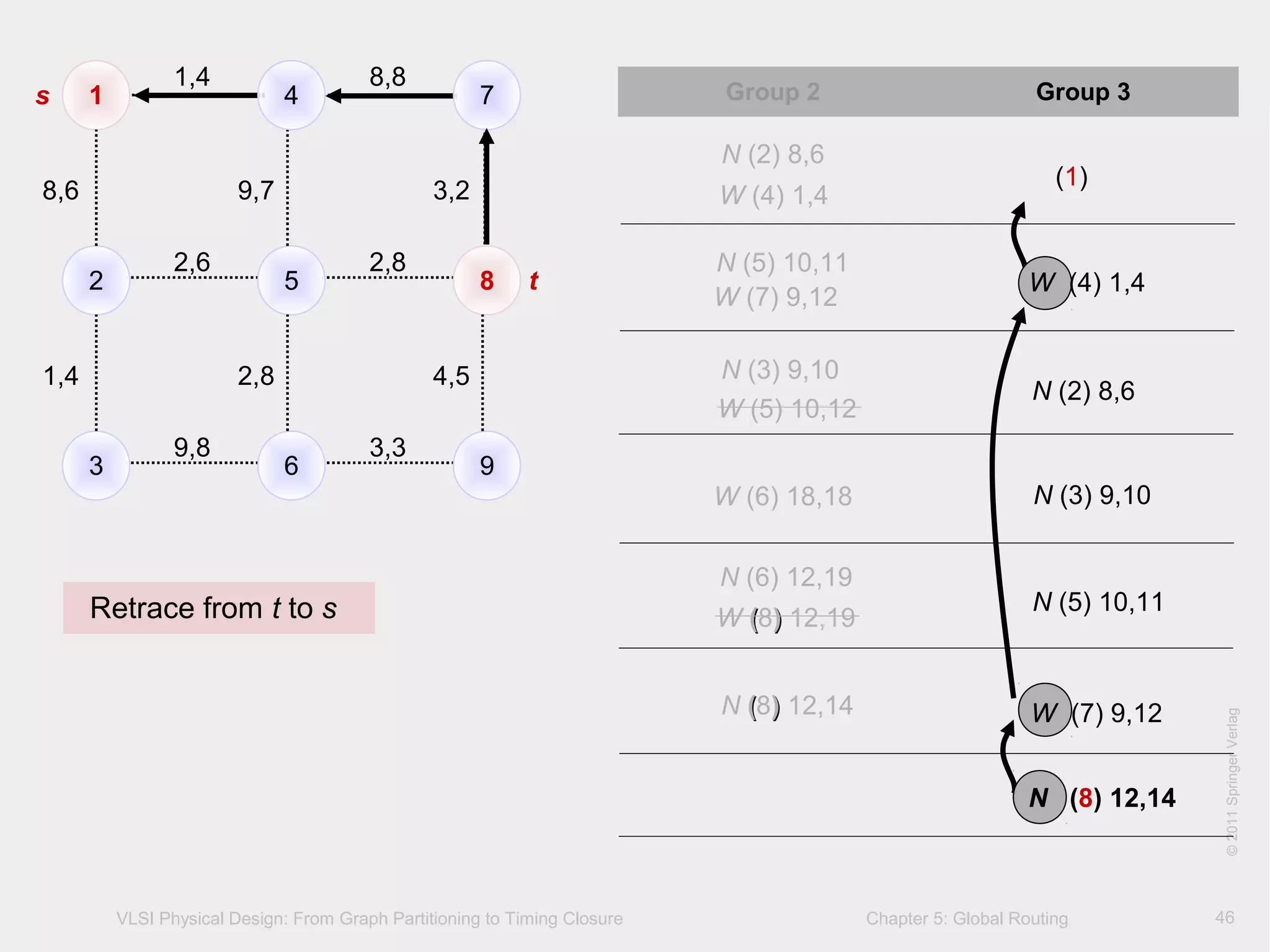
N (8) 12,14
Current node: 7
Neighboring nodes: 4, 8
Minimum cost in group 2: node 8
s
t
parent of node [node name] ∑w1(s,node),∑w2(s,node)](https://image.slidesharecdn.com/cadglobalrouting-140705013857-phpapp02/75/Computer-Aided-Design-Global-Routing-45-2048.jpg)


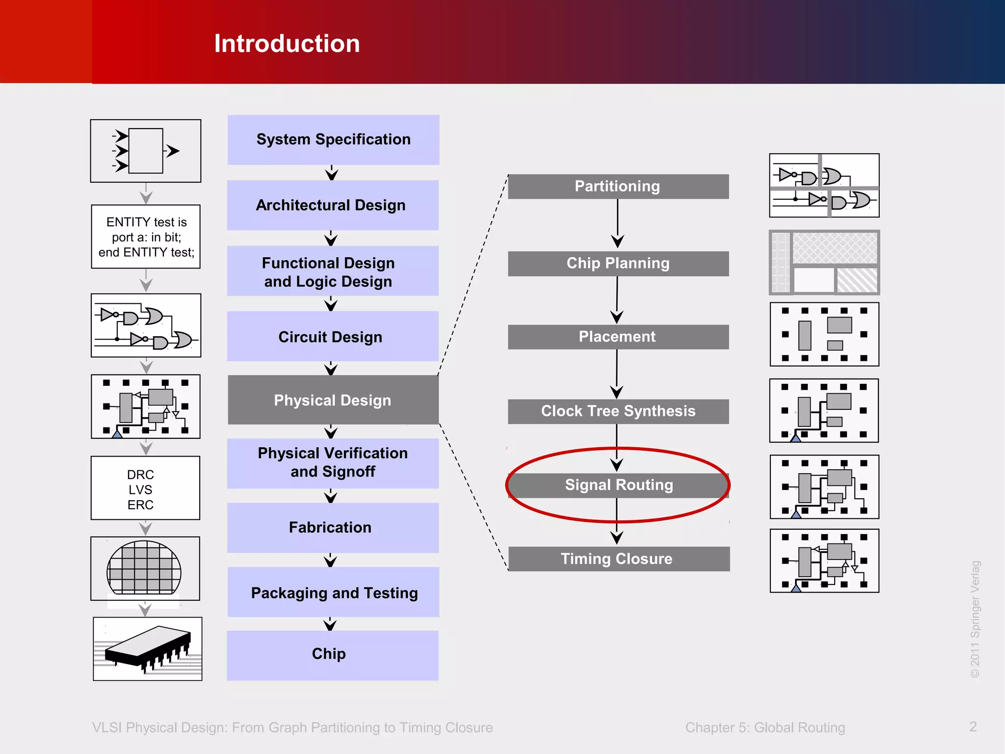
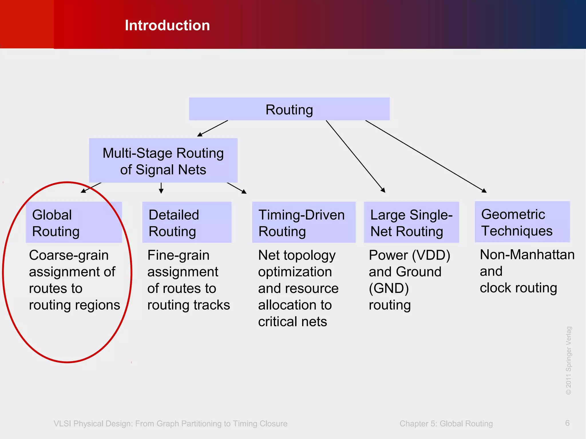
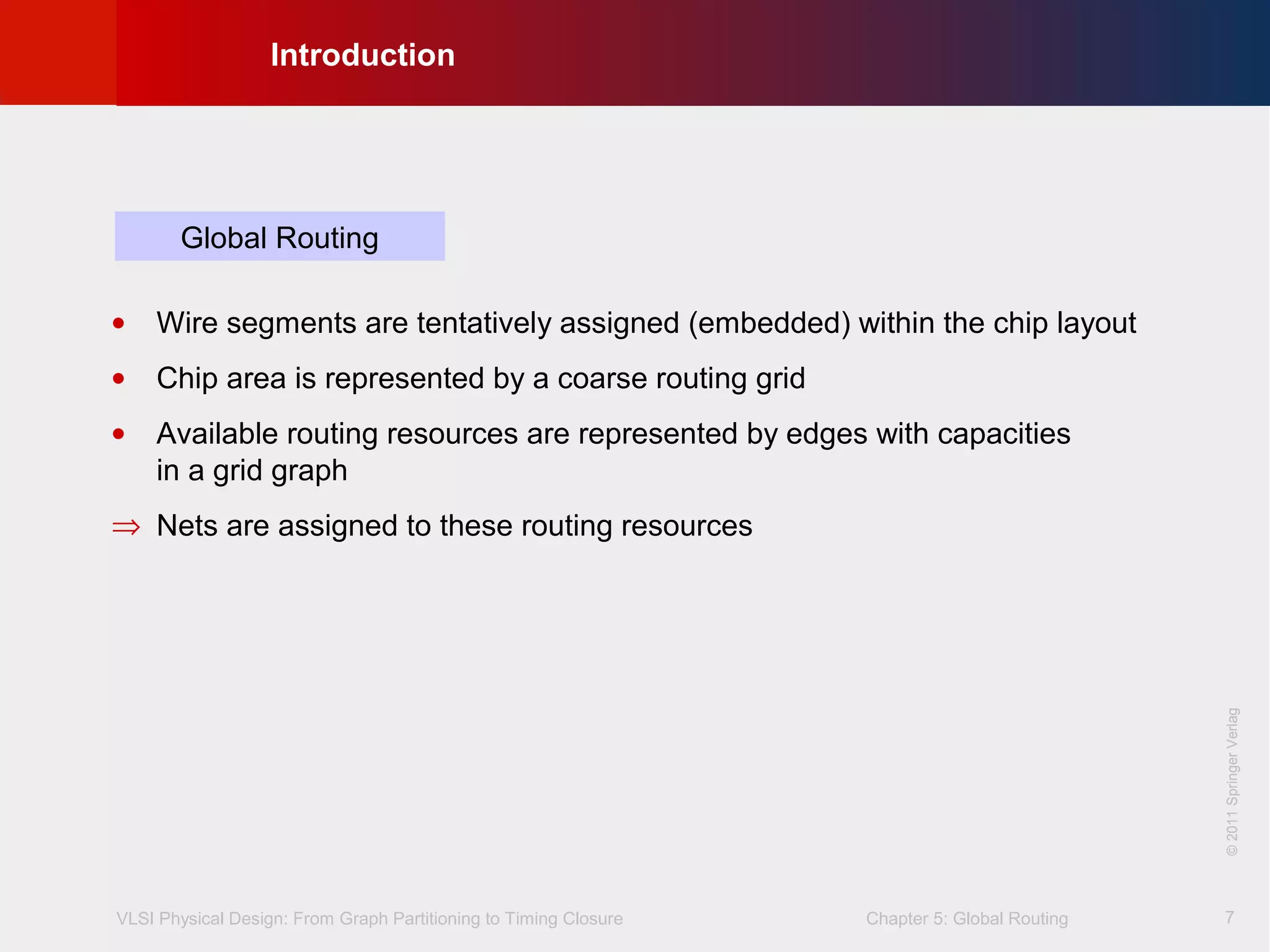
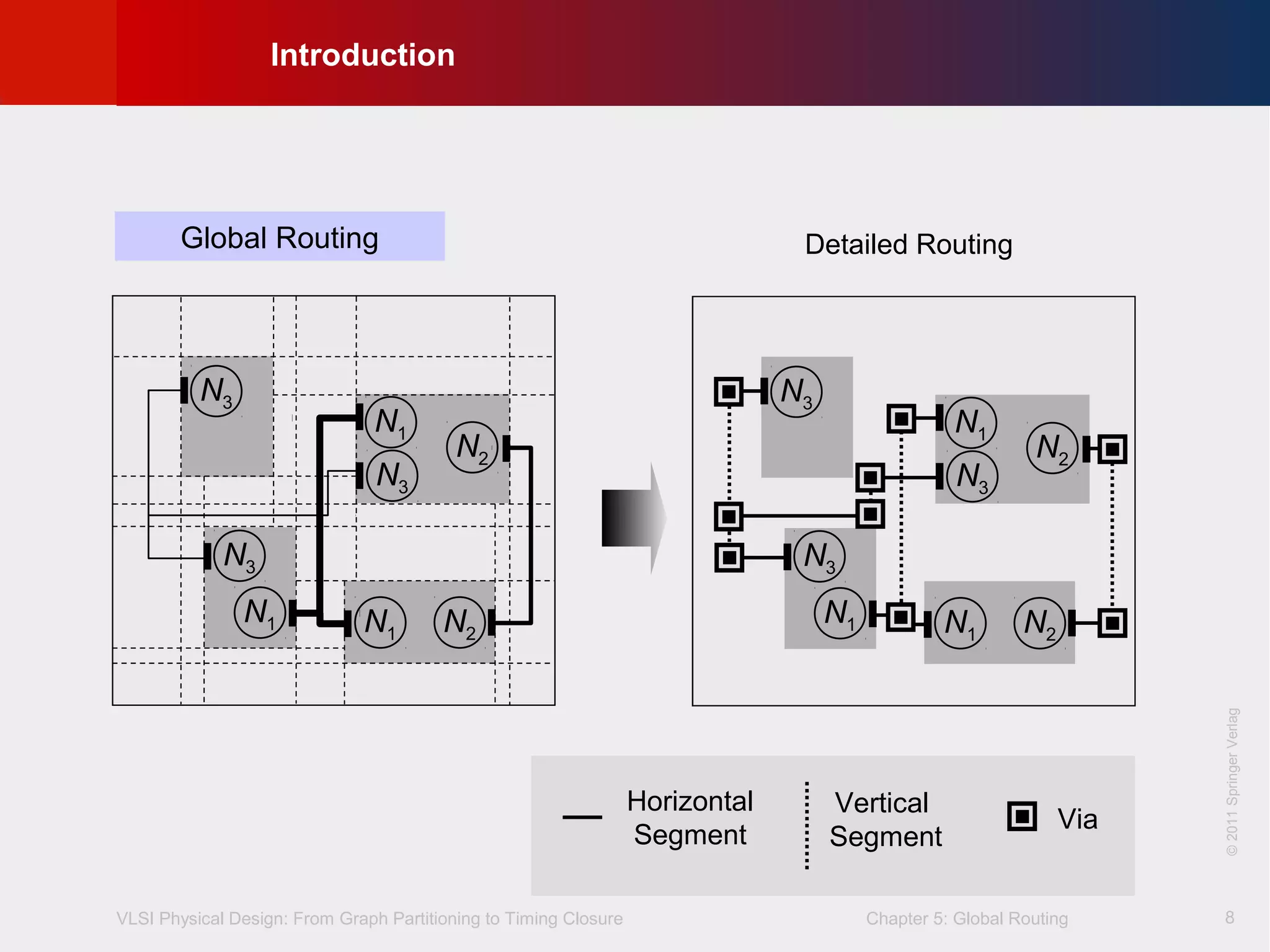
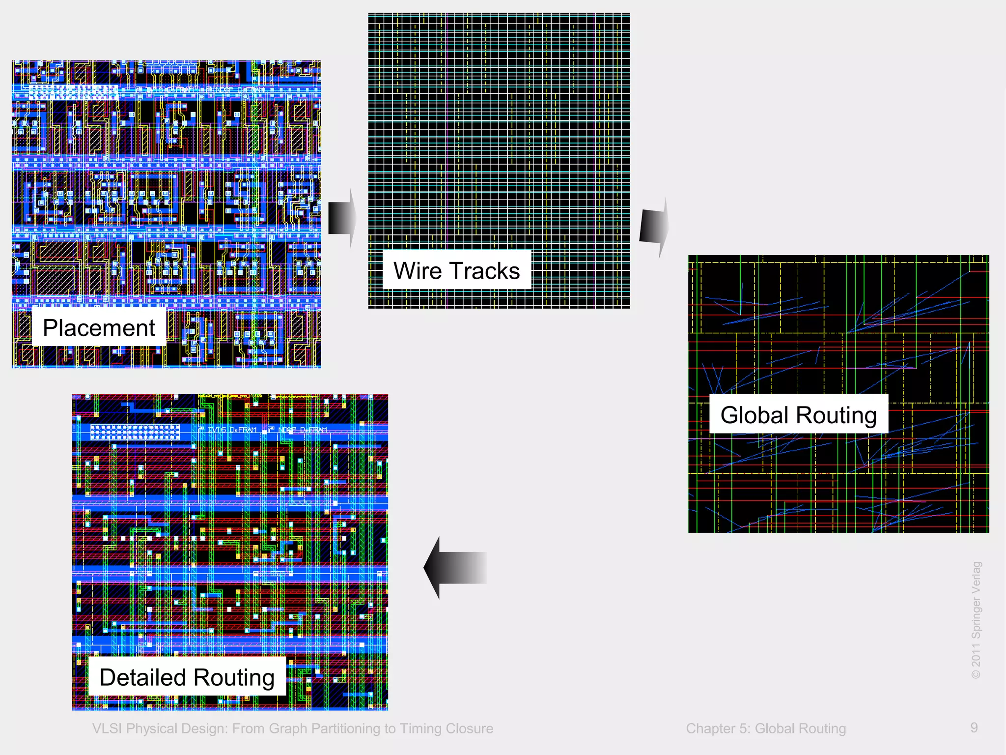
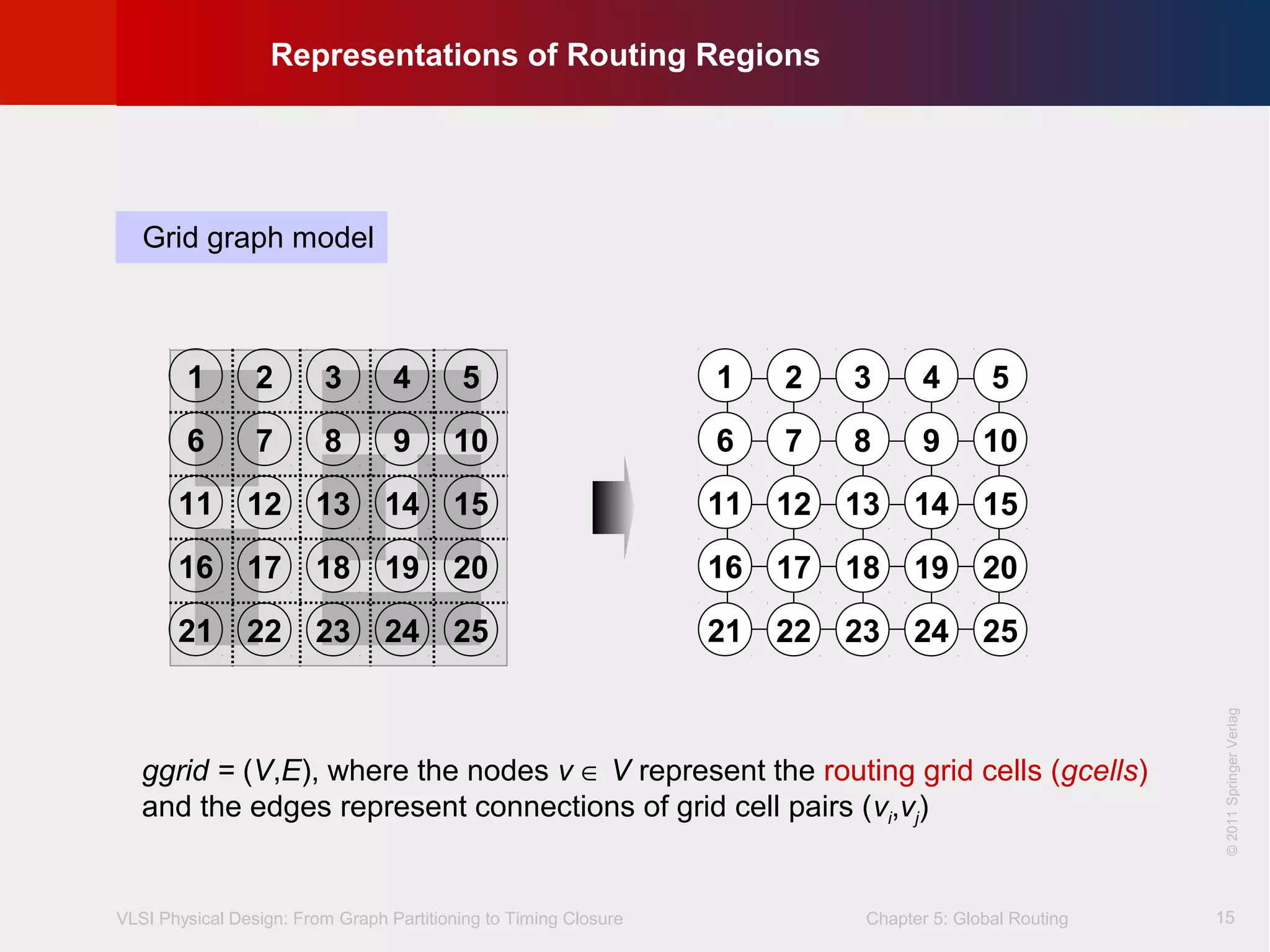
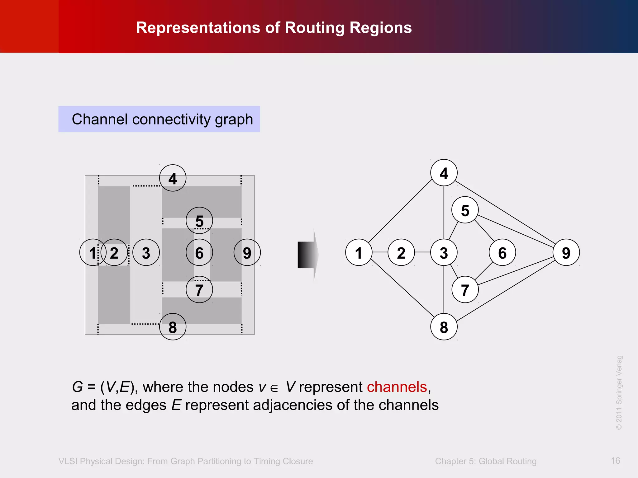
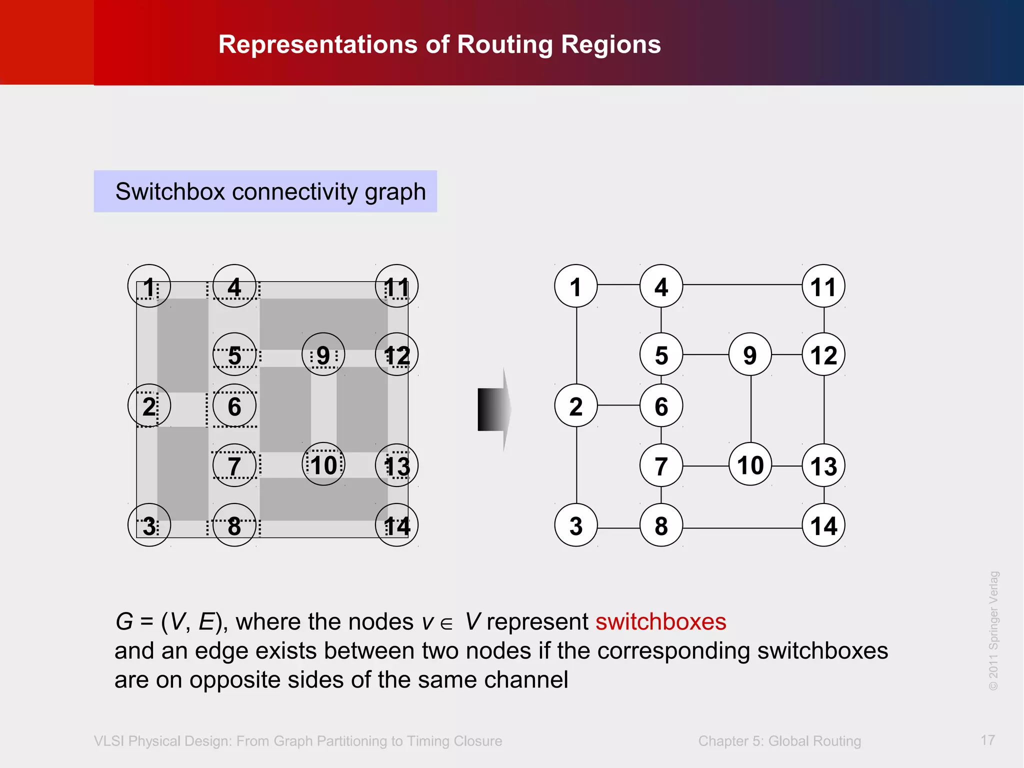
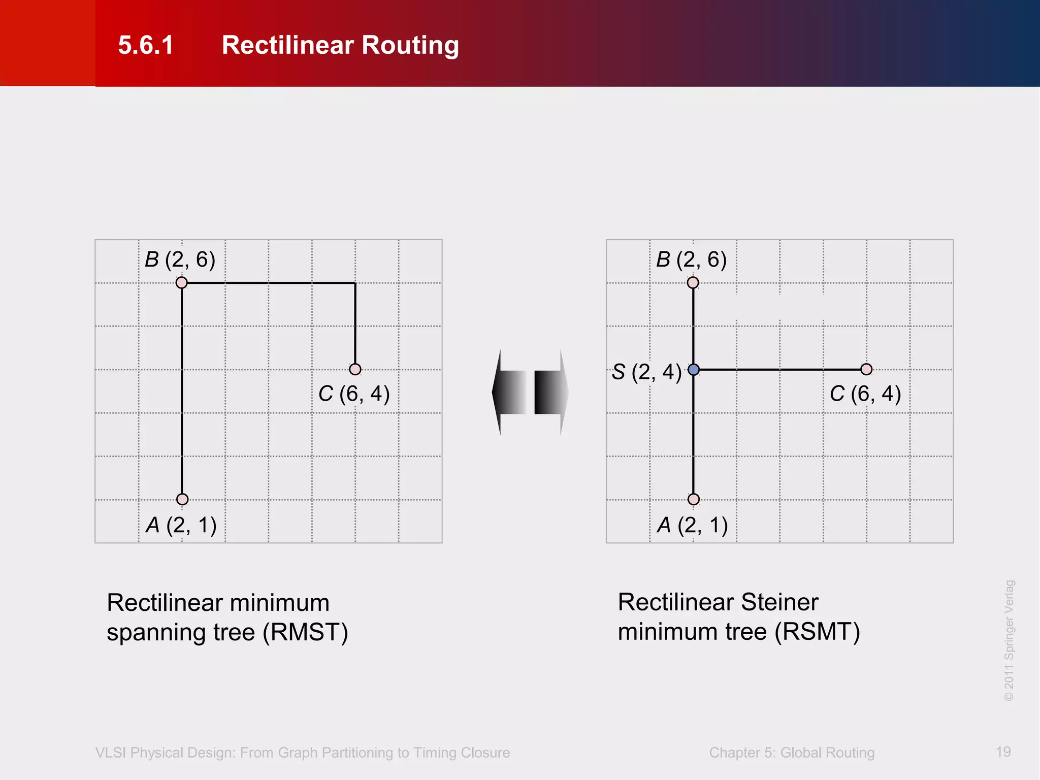
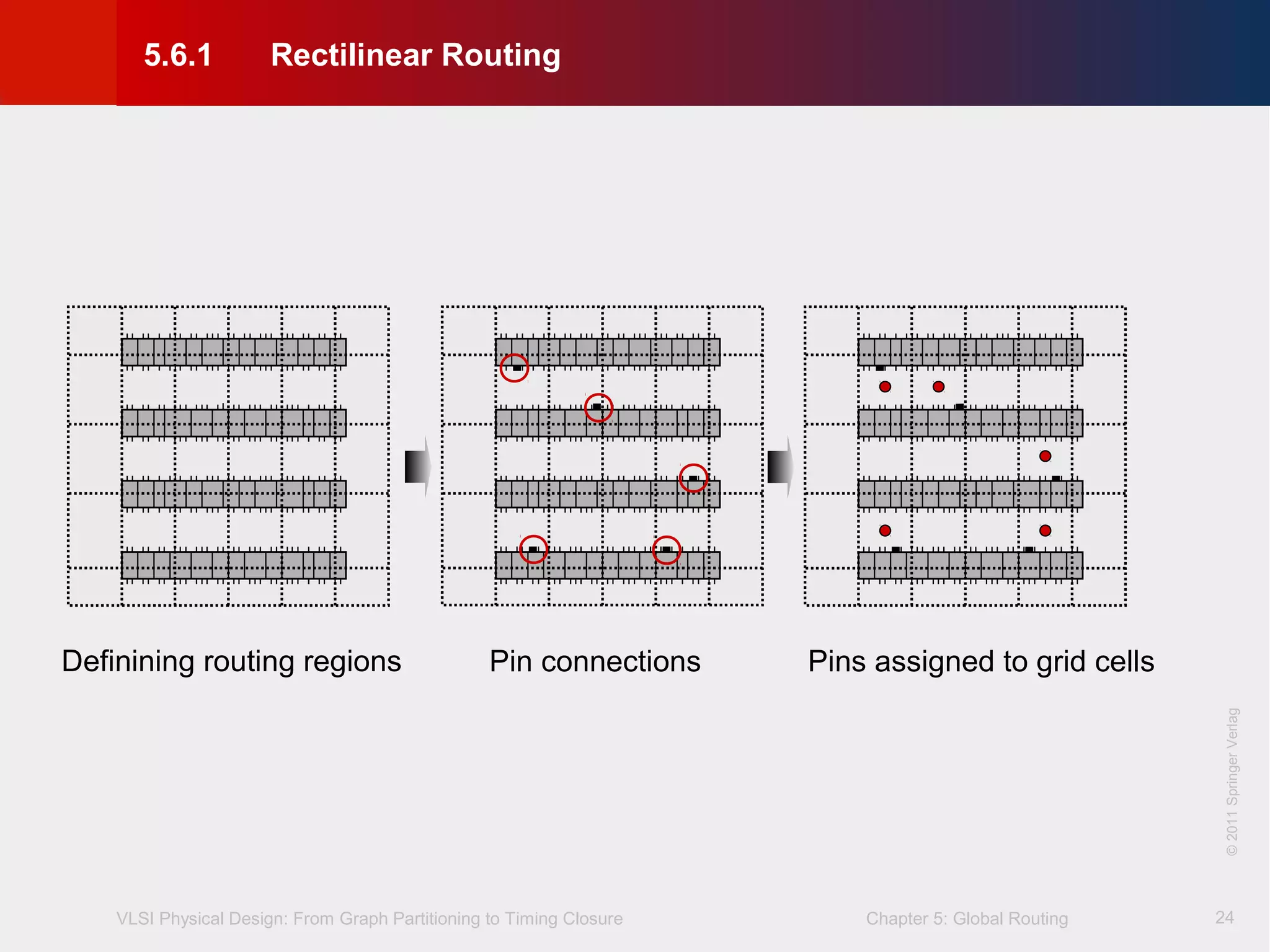
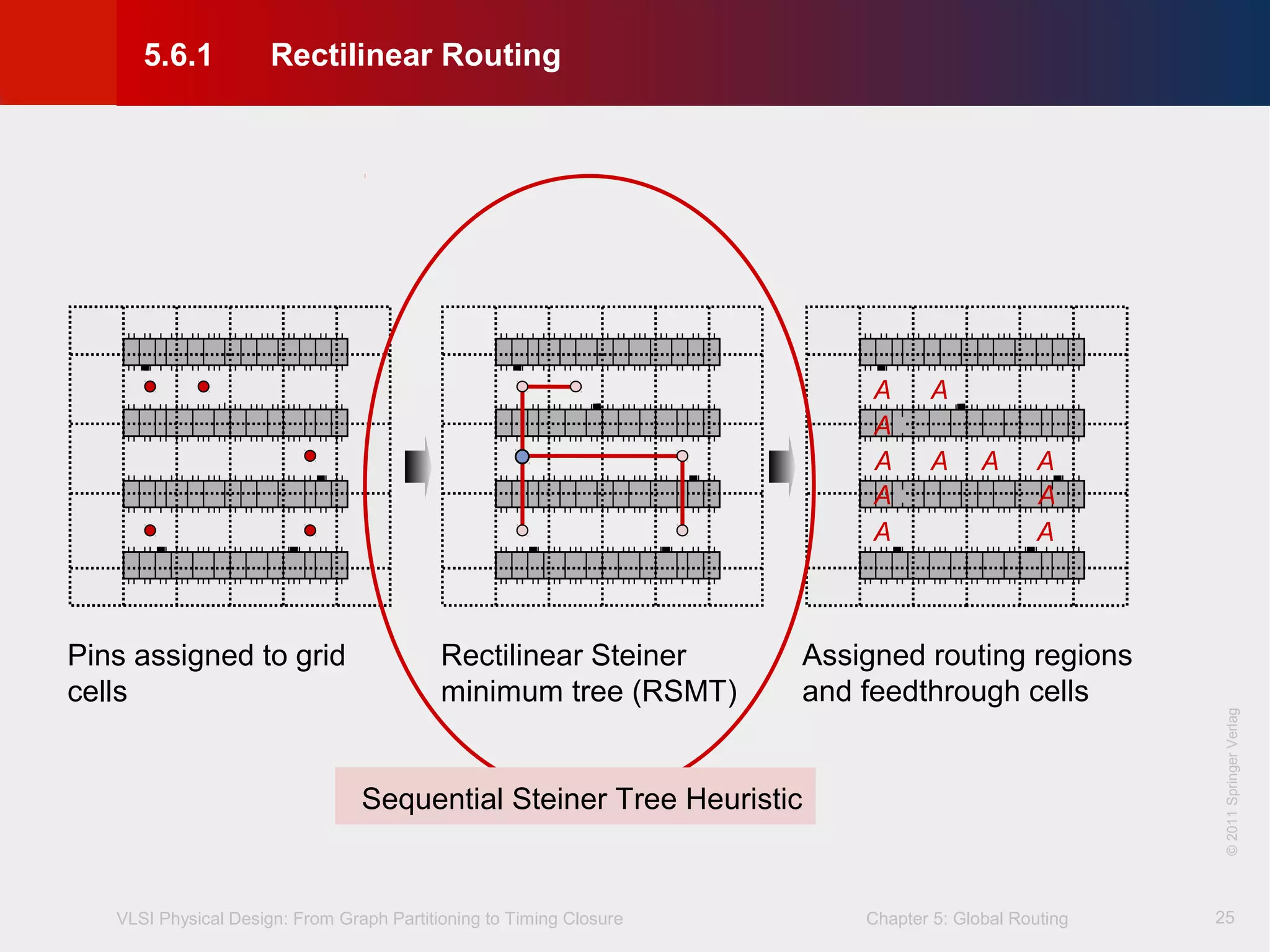
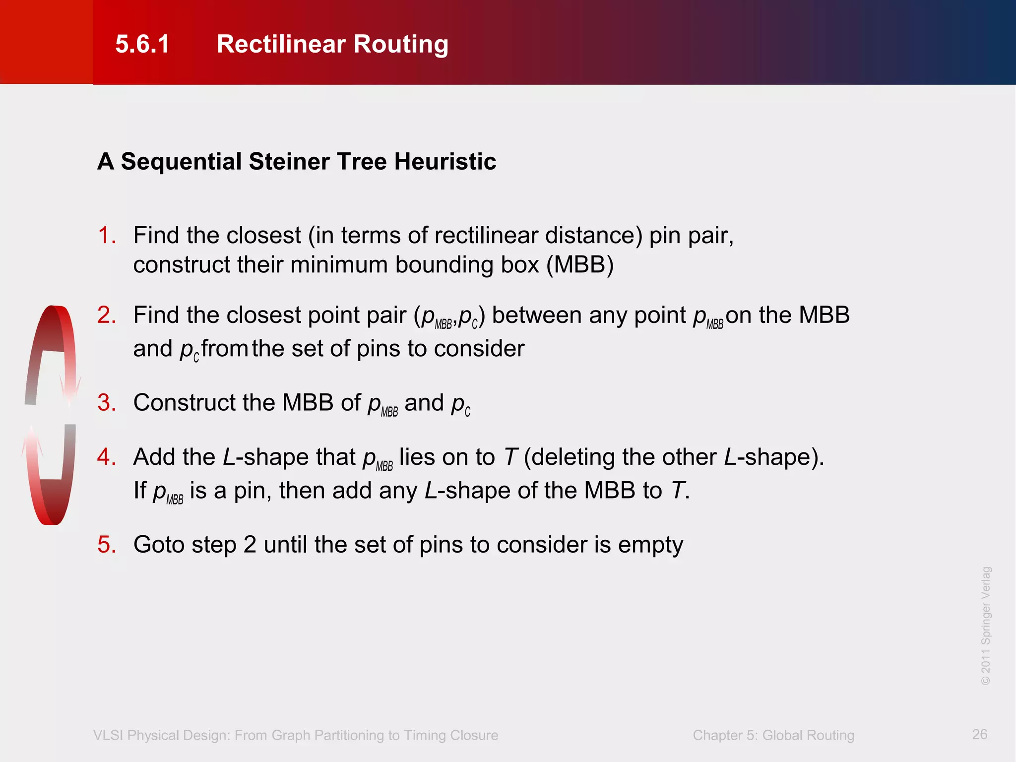
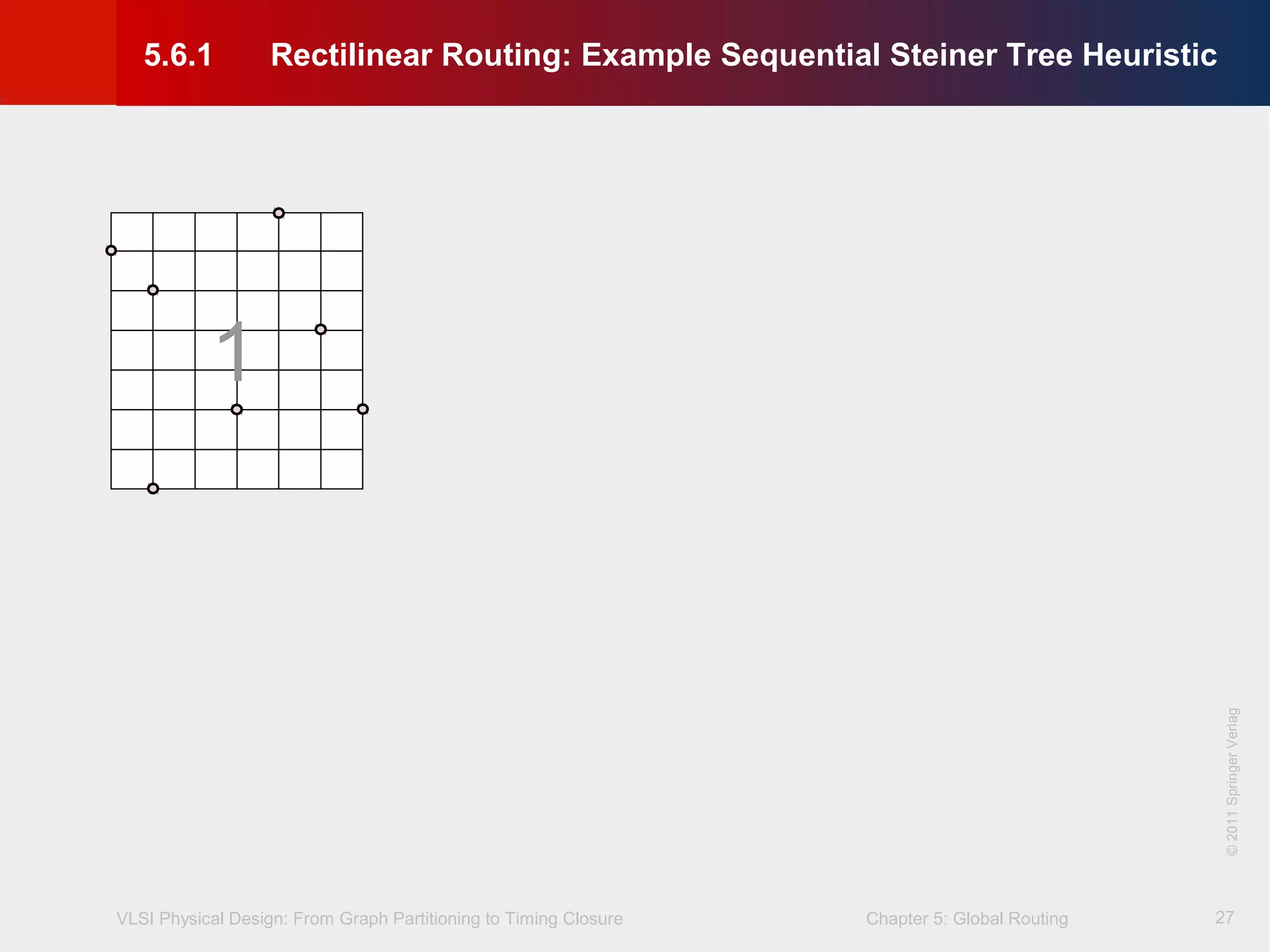
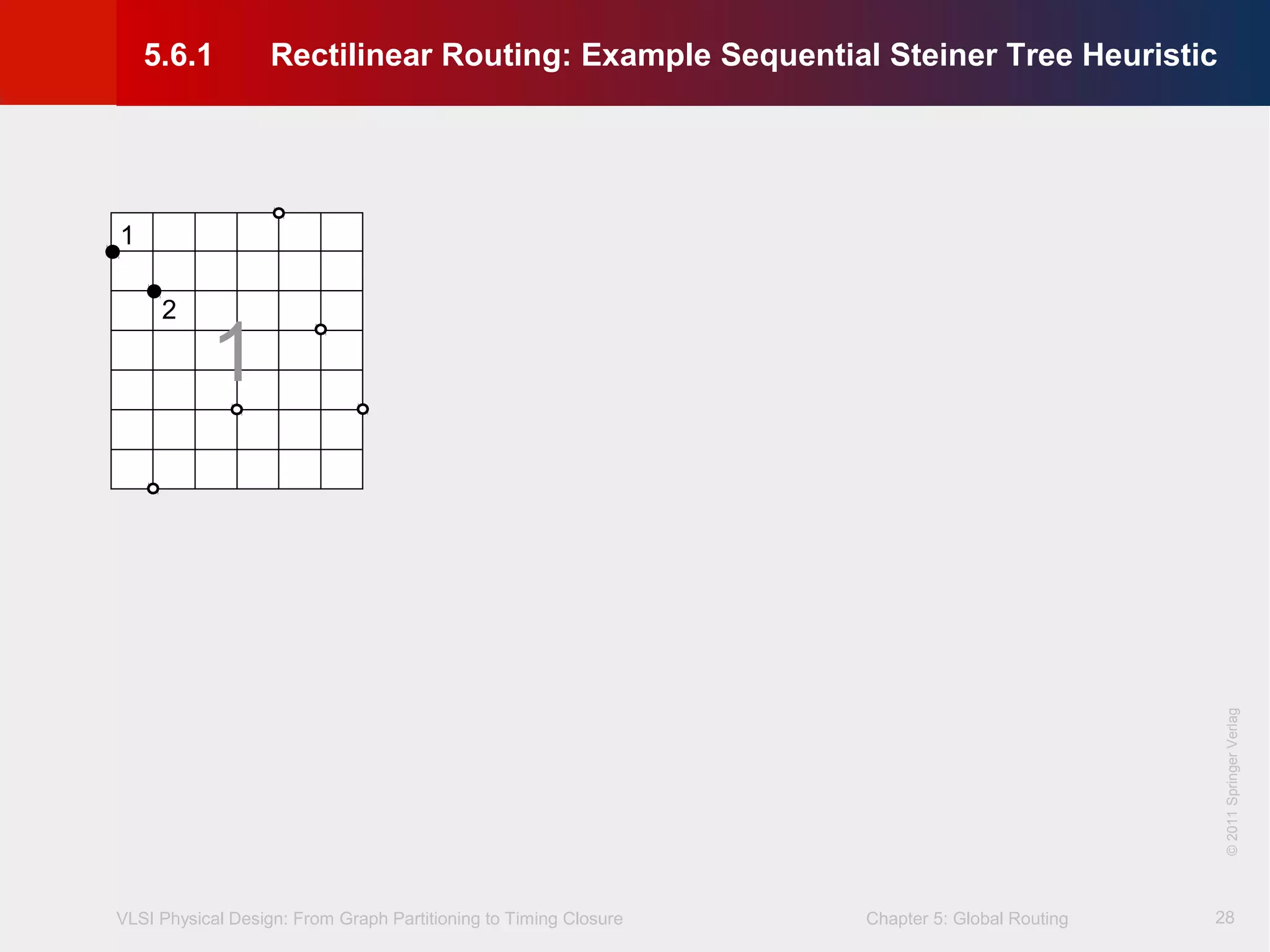
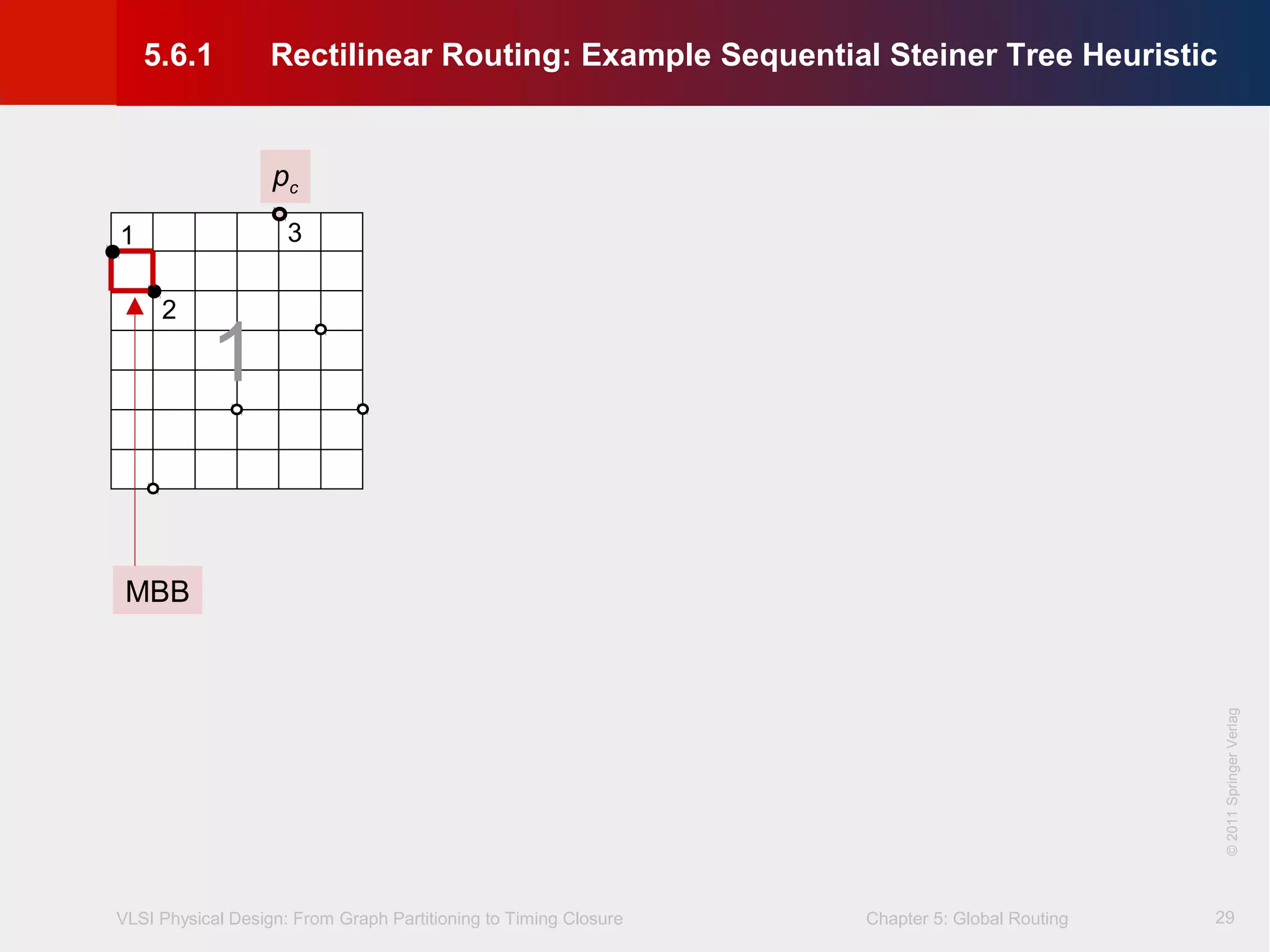
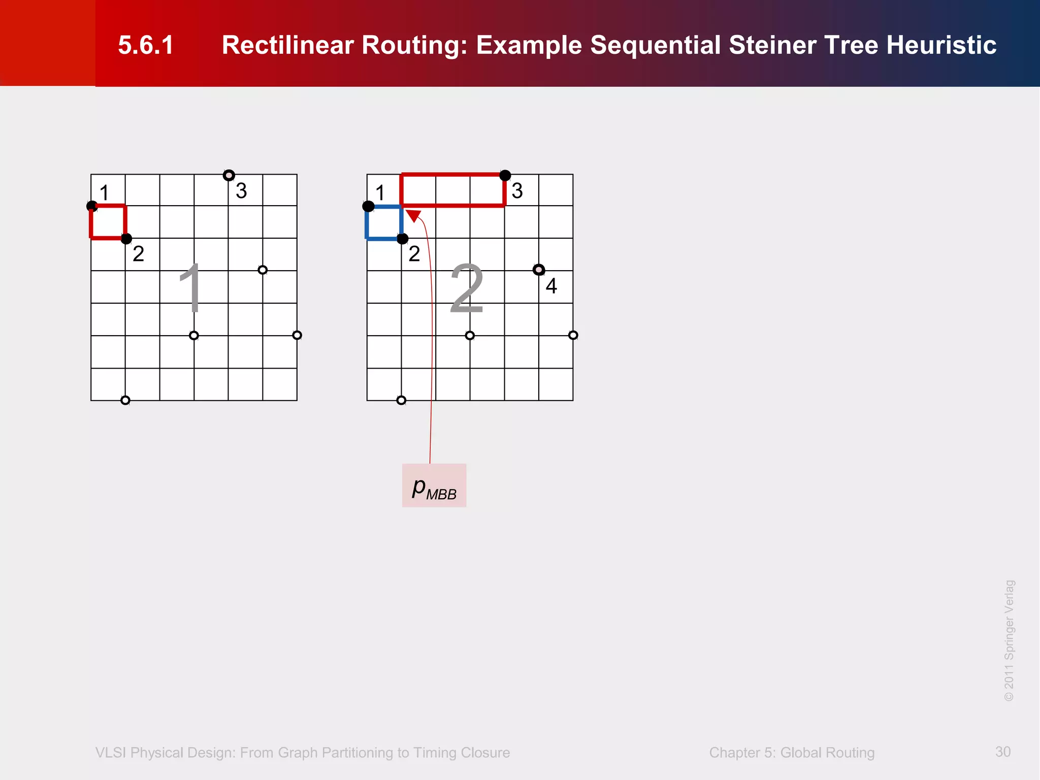
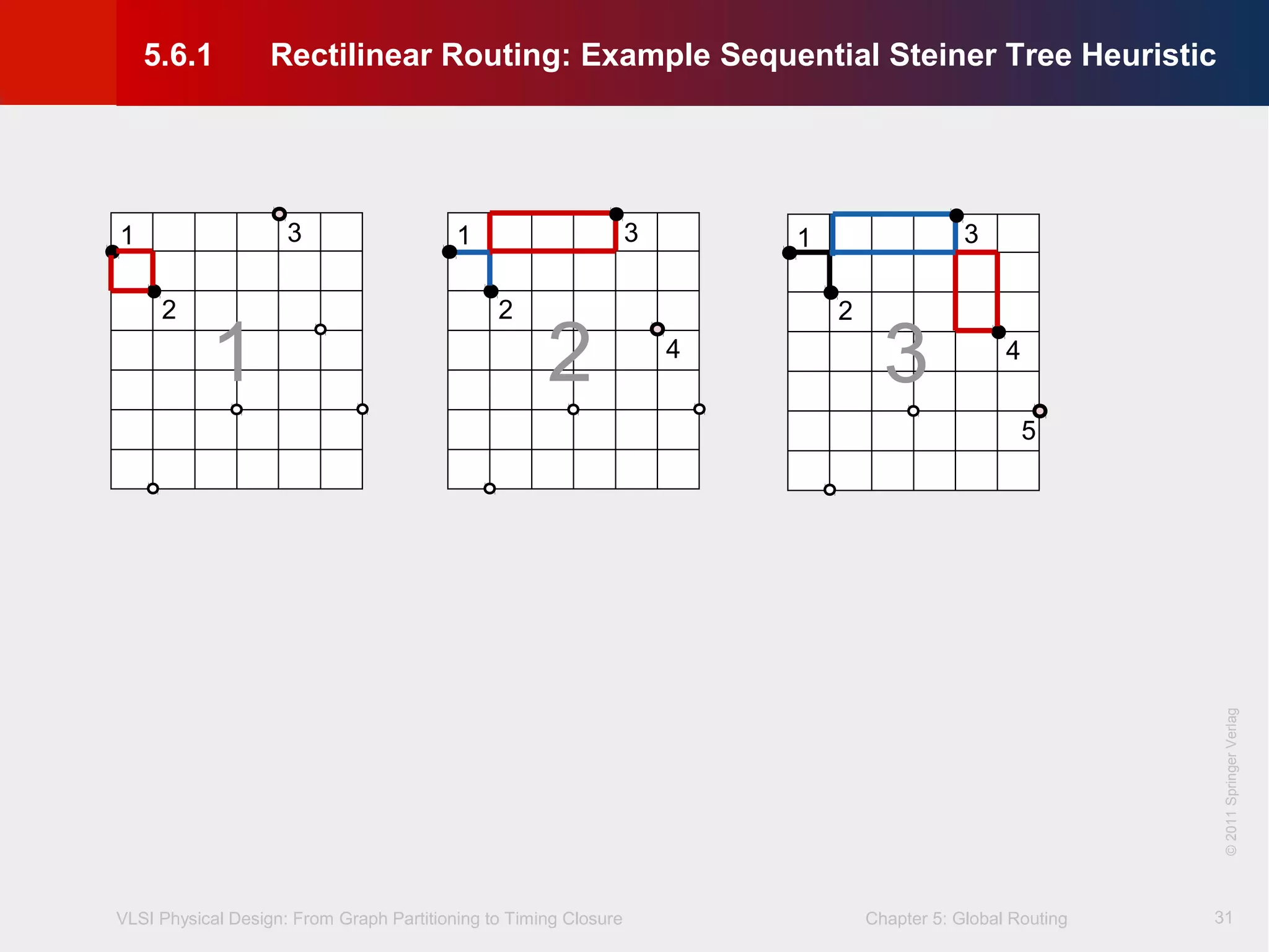
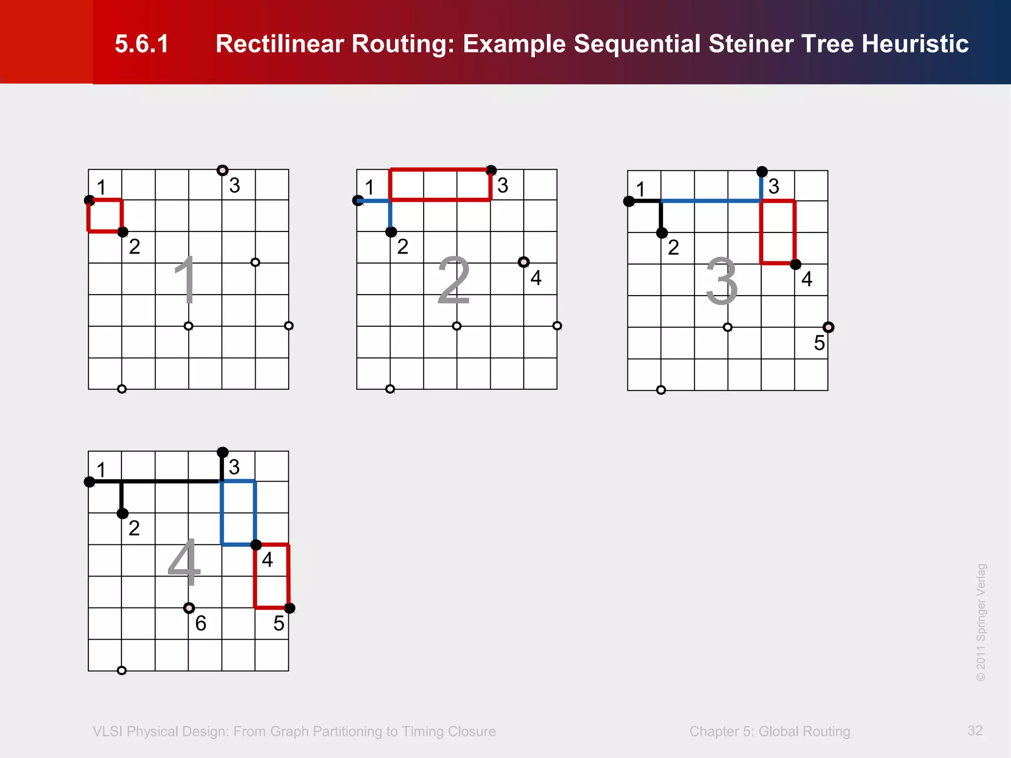
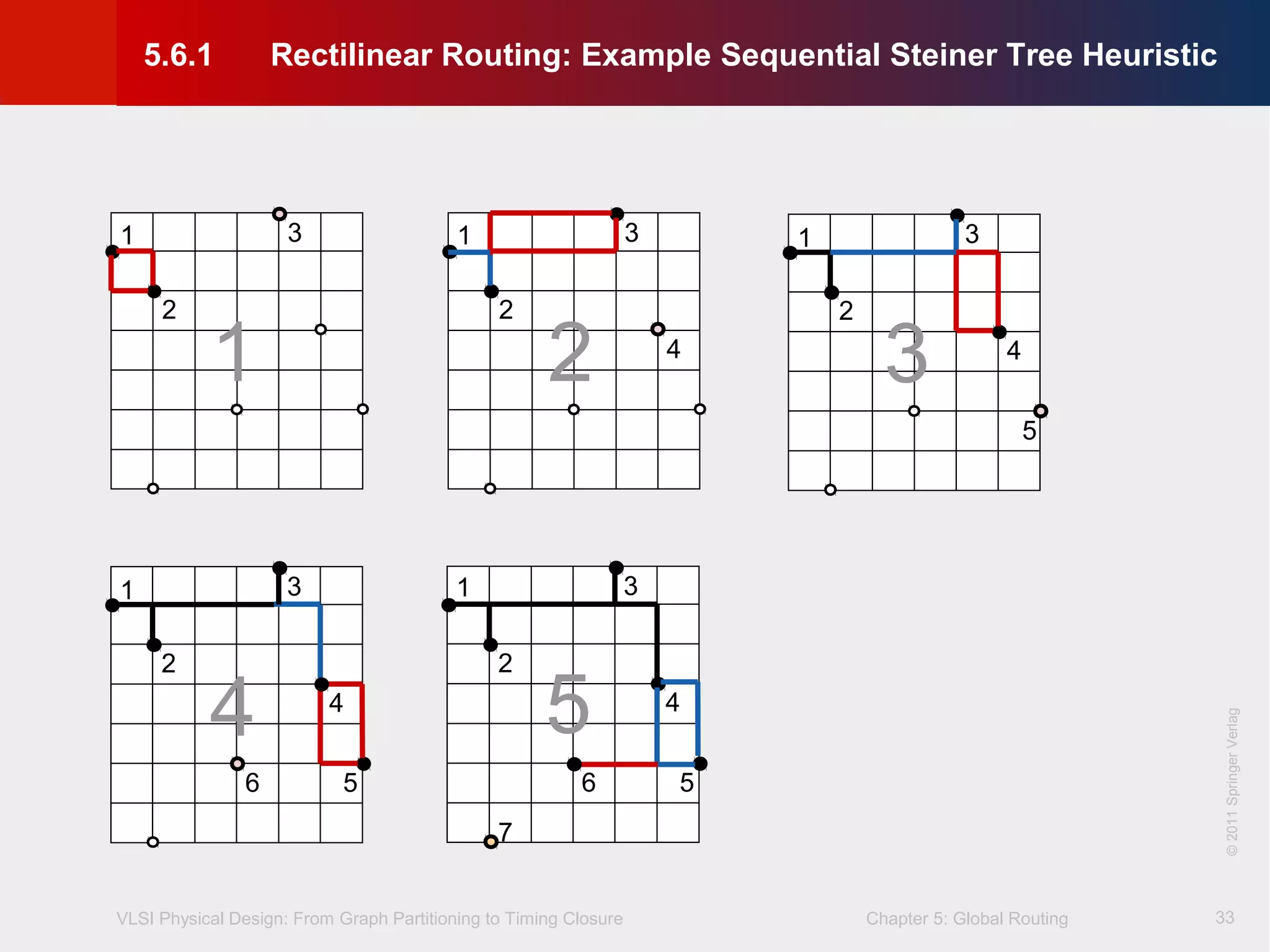
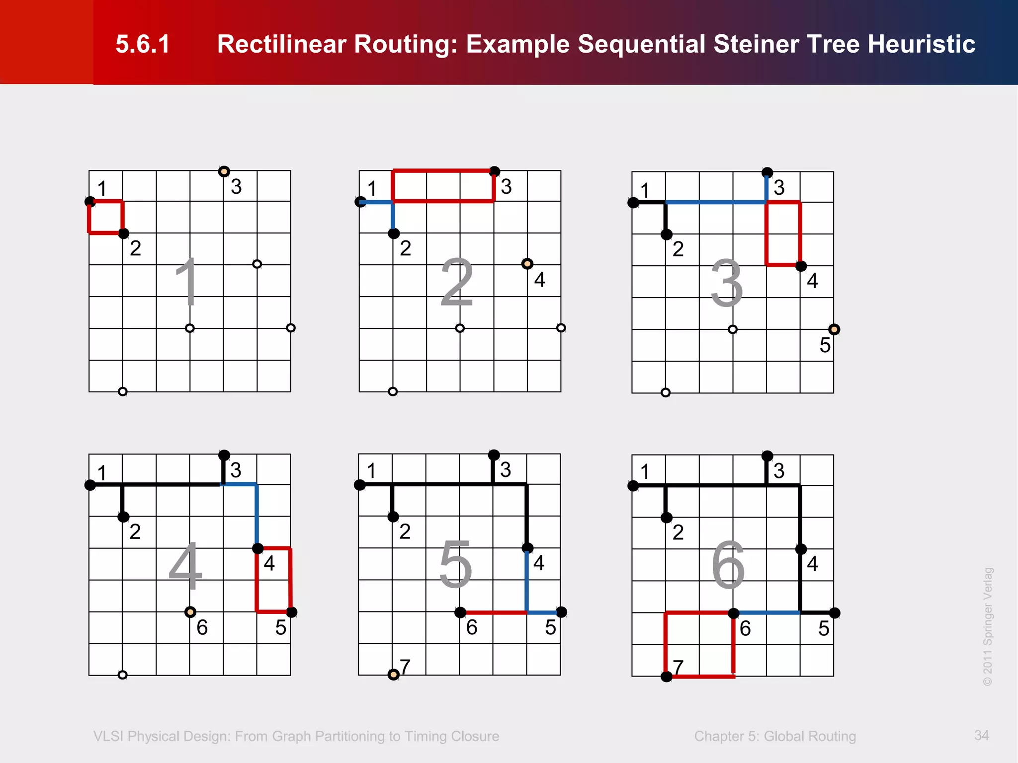
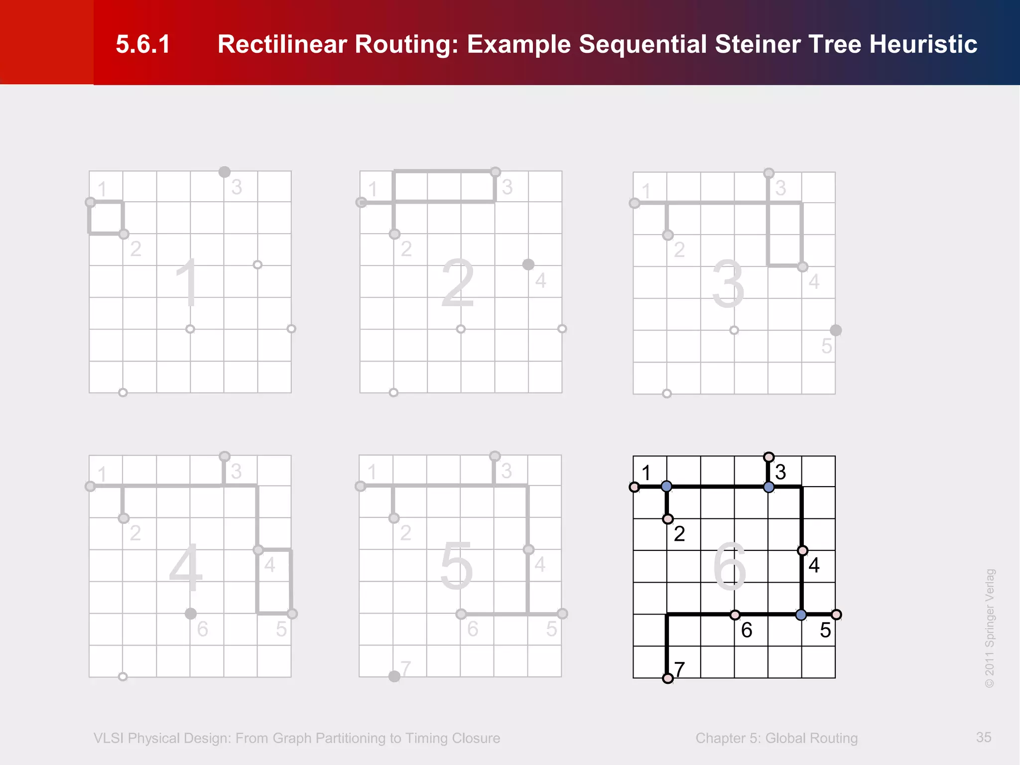
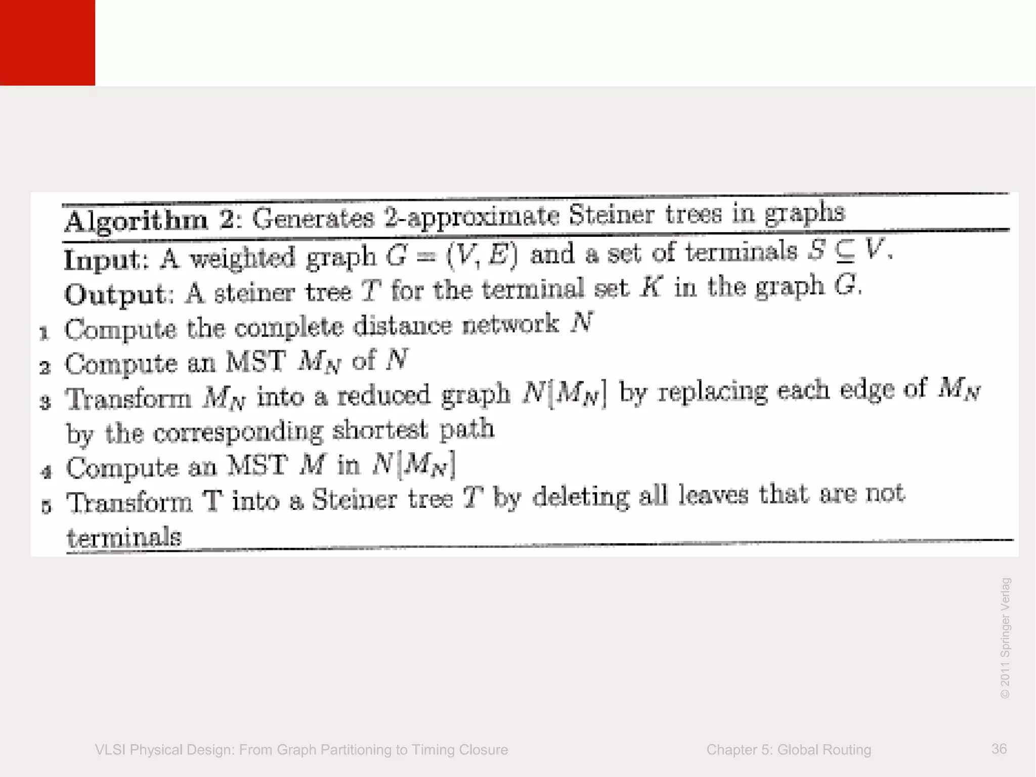
This document describes the process of global routing in VLSI physical design. Global routing assigns wiring paths between circuit components at a coarse level of granularity by partitioning the chip into routing regions and assigning nets to these regions. It aims to minimize total wirelength and reduce delays on critical nets. Routing regions are represented using graphs to model available routing resources. Common algorithms discussed include rectilinear Steiner tree construction and sequential Steiner tree heuristics to find minimum path routes between pins in the global routing stage.