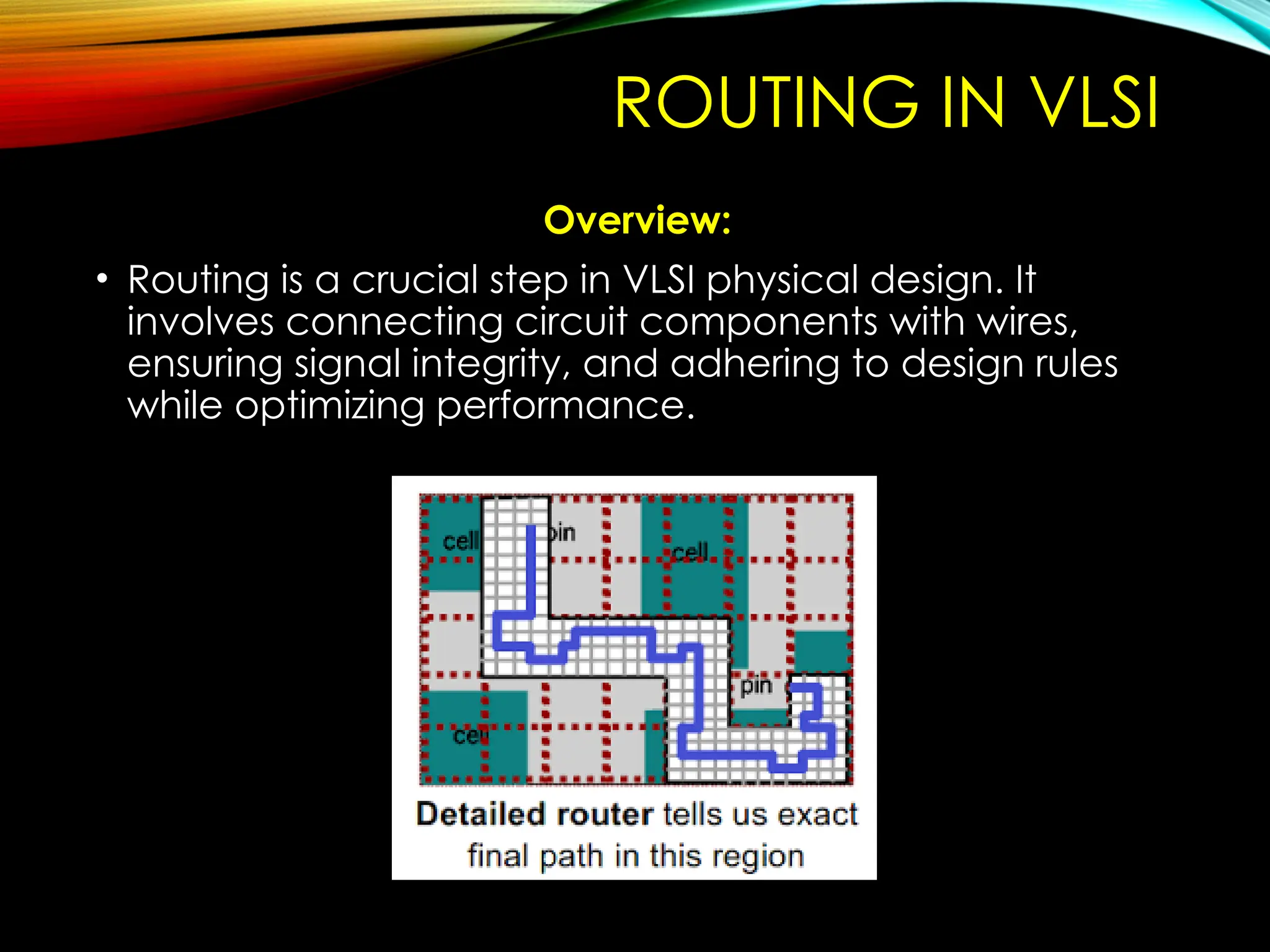
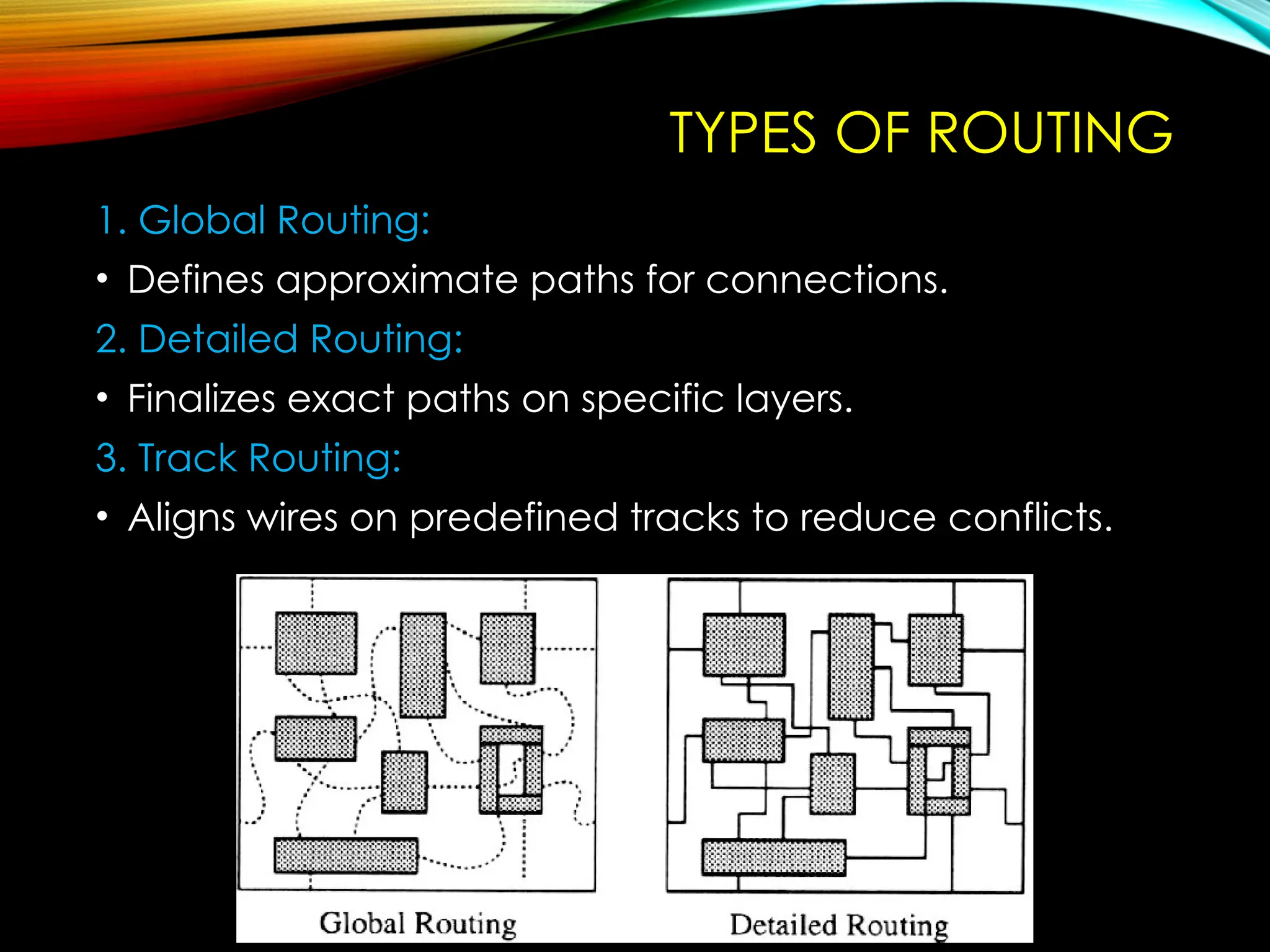
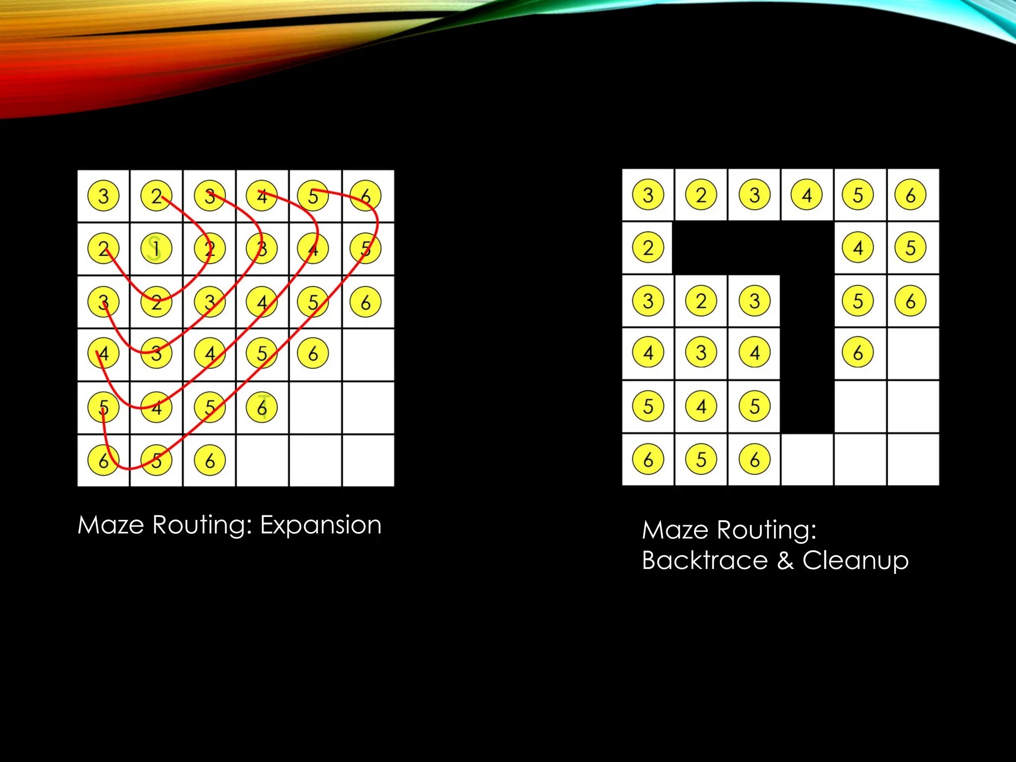
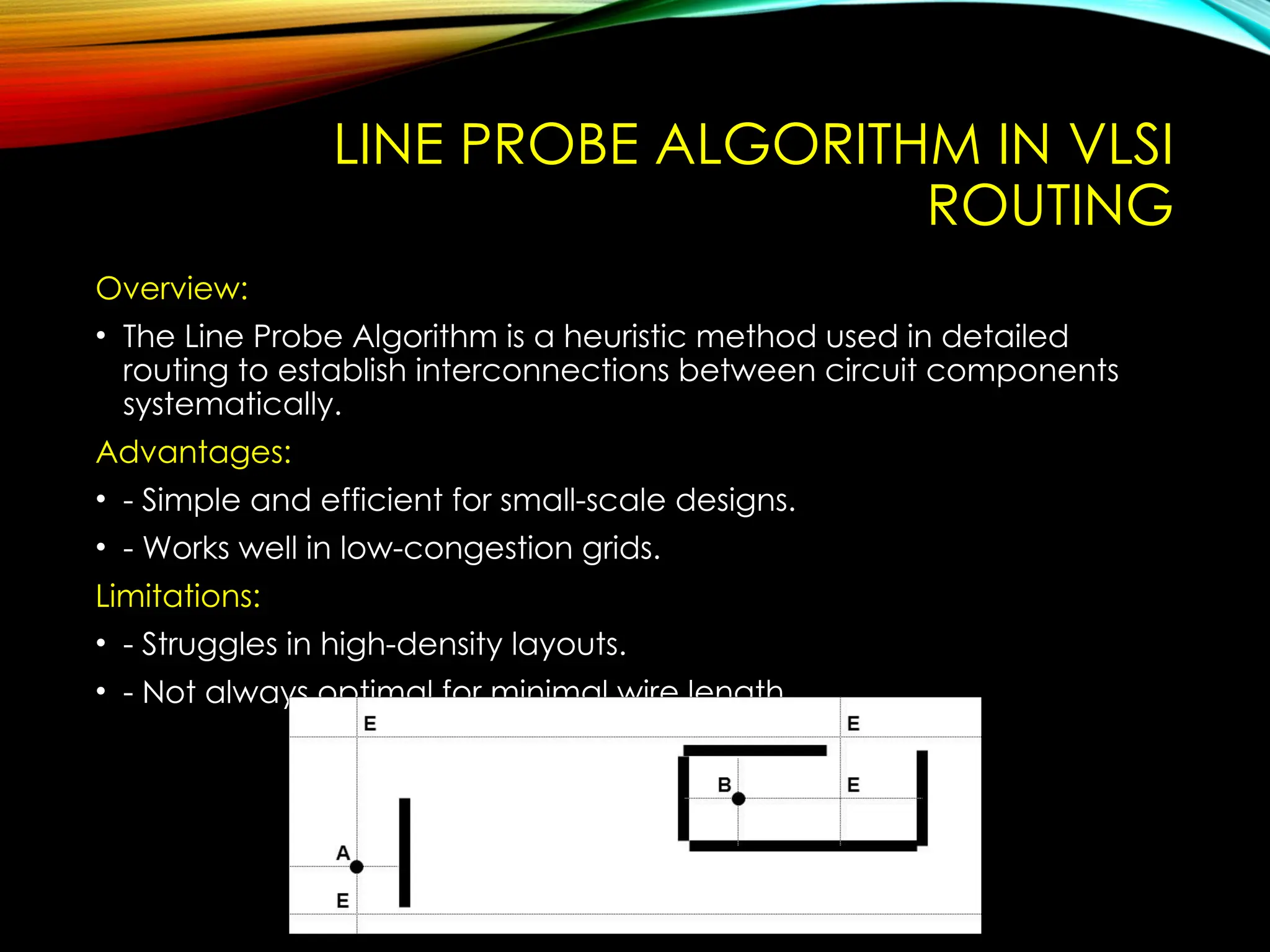
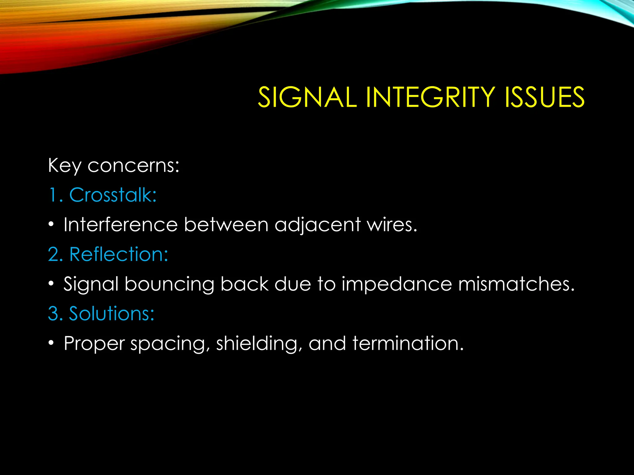
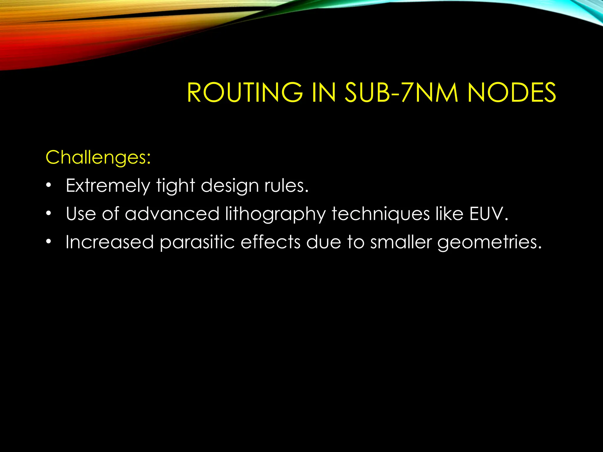
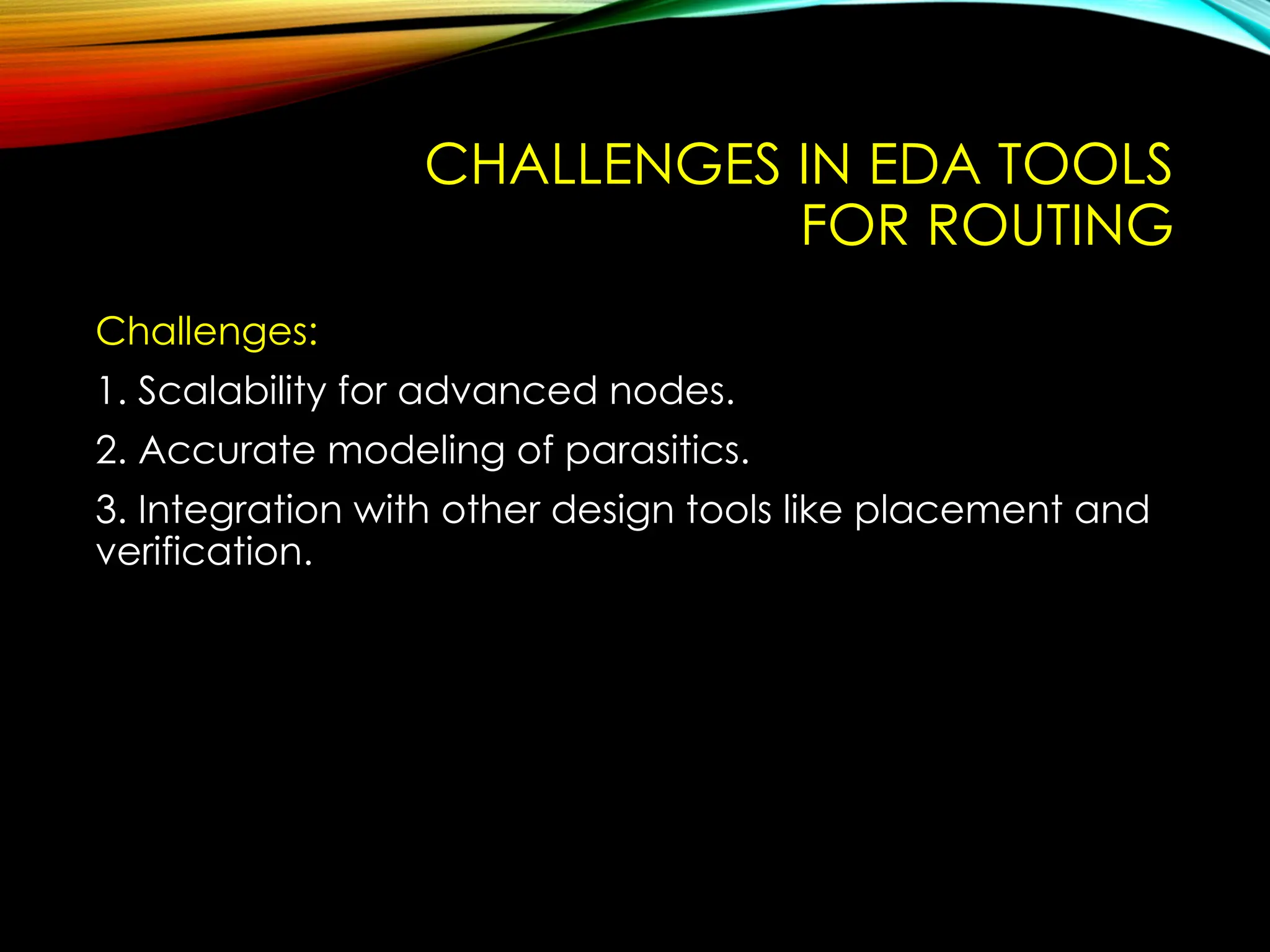
ROUTING IN VLSI
Overview:
• Routing is a crucial step in VLSI physical design. It
involves connecting circuit components with wires,
ensuring signal integrity, and adhering to design rules
while optimizing performance.
INTRODUCTION TO ROUTING
Definition:
• Routing determines electrical paths for interconnecting
circuit components. This process directly impacts chip
performance, power, and area.
• It is a critical step in the physical design phase, ensuring
proper signal transmission across the chip while
adhering to design rules and constraints.
IMPORTANCE OF ROUTING IN VLSI
• Routing ensures:
• - Signal integrity by minimizing interference.
• - Efficient use of chip area.
• - Reduced delay and power consumption.
• - Compliance with manufacturing design rules.
TYPES OF ROUTING
1. Global Routing:
• Defines approximate paths for connections.
2. Detailed Routing:
• Finalizes exact paths on specific layers.
3. Track Routing:
• Aligns wires on predefined tracks to reduce conflicts.
CHALLENGES IN ROUTING
1. Congestion:
• Ensuring all connections fit in limited space.
2. Crosstalk:
• Minimizing interference between adjacent wires.
3. Timing Issues:
• Meeting delay constraints for critical signals.
ROUTING TECHNIQUES
1. Maze Routing:
• Finds a path using breadth-first search.
2. Line Probe Algorithm:
• Explores potential paths systematically.
3. Steiner Tree:
• Minimizes wire length for multiple connections.
MAZE ROUTING
Details:
• Maze Routing uses a grid-based approach to find the shortest path between
two points while avoiding obstacles. It is computationally intensive.
Advantages:
• Guaranteed Solution: If a path exists between the source and target, Maze
Routing will find it.
• Flexibility: Works well in grids with complex obstacles or constraints.
• Applicability: Can handle various grid-based layouts and accommodate
multiple layers.
Limitations:
• Computationally Intensive: The algorithm is slow for large grids as it requires
exploring all possible paths.
• Suboptimal Paths: The shortest path may not always be the best in terms of
performance metrics like delay or congestion.
• Scalability Issues: Becomes inefficient for modern, high-density designs.
Maze Routing: Expansion Maze Routing:
Backtrace & Cleanup
LINE PROBE ALGORITHM IN VLSI
ROUTING
Overview:
• The Line Probe Algorithm is a heuristic method used in detailed
routing to establish interconnections between circuit components
systematically.
Advantages:
• - Simple and efficient for small-scale designs.
• - Works well in low-congestion grids.
Limitations:
• - Struggles in high-density layouts.
• - Not always optimal for minimal wire length.
STEINER TREE ROUTING
Details:
• The Steiner Tree algorithm connects multiple points using the minimum possible wire
length, reducing interconnect delays.
Advantages:
• Minimized Wirelength: It reduces the total wire length for multi-terminal nets, improving
area and performance.
• Optimized Delay: Shorter interconnects reduce signal propagation delay.
• Efficient Use of Resources: Helps in managing limited routing resources in high-density
layouts.
Limitations:
• Complexity: Generating an optimal Steiner Tree is computationally expensive (NP-hard
problem).
• Signal Integrity Concerns: Optimizing for wire length can lead to narrower wires or
reduced spacing, increasing crosstalk and interference risks.
• Routing Overhead: May require additional post-processing to meet practical design
rules.
DESIGN RULES IN ROUTING
Design rules include:
• - Minimum spacing between wires to prevent shorts.
• - Minimum wire width for reliable current flow.
• - Specific rules for each layer (e.g., metal layers).
ROUTING TOOLS IN VLSI
Popular tools:
• 1. Cadence Innovus
• 2. Synopsys IC Compiler
• 3. Mentor Graphics Calibre
These tools handle routing, verification, and optimization.
OPTIMIZATION TECHNIQUES IN
ROUTING
Key optimizations:
• Clock Tree Synthesis (CTS) ensures balanced clock
signal distribution.
• Delay balancing minimizes signal skew.
• Shielding critical nets prevents interference.
SIGNAL INTEGRITY ISSUES
Key concerns:
1. Crosstalk:
• Interference between adjacent wires.
2. Reflection:
• Signal bouncing back due to impedance mismatches.
3. Solutions:
• Proper spacing, shielding, and termination.
ROUTING IN SUB-7NM NODES
Challenges:
• Extremely tight design rules.
• Use of advanced lithography techniques like EUV.
• Increased parasitic effects due to smaller geometries.
POWER AND AREA
OPTIMIZATION IN ROUTING
Strategies:
1. Shorter wires reduce power consumption.
2. Efficient use of routing layers minimizes chip area.
3. Tools like power-aware routing optimize power
distribution.
APPLICATIONS OF ROUTING IN
VLSI
Applications include:
• - High-speed processors for computing.
• - Memory chips for data storage.
• - RF circuits for communication systems.
FUTURE OF ROUTING IN VLSI
Emerging trends:
• AI-driven routing optimization.
• Use of quantum computing for routing algorithms.
• Enhanced materials for interconnects like graphene.
CHALLENGES IN EDA TOOLS
FOR ROUTING
Challenges:
1. Scalability for advanced nodes.
2. Accurate modeling of parasitics.
3. Integration with other design tools like placement and
verification.
CONCLUSION
Summary:
• Routing is a pivotal step in VLSI design, bridging the gap
between logical connectivity and physical implementation.
Effective routing ensures reliable electrical performance,
minimal delay, and optimal power usage, all while adhering
to stringent design rules. With advancements in technology
scaling and increasing design complexity, innovative routing
techniques and tools are essential to address challenges like
congestion, crosstalk, and signal integrity. As VLSI design
continues to evolve, routing will remain a cornerstone in
achieving high-performance, power-efficient, and area-
optimized chips for modern applications.
THANK YOU

Routing_process_in_VLSI_verilogmodeling.pptx

  • 2.
    ROUTING IN VLSI Overview: •Routing is a crucial step in VLSI physical design. It involves connecting circuit components with wires, ensuring signal integrity, and adhering to design rules while optimizing performance.
  • 3.
    INTRODUCTION TO ROUTING Definition: •Routing determines electrical paths for interconnecting circuit components. This process directly impacts chip performance, power, and area. • It is a critical step in the physical design phase, ensuring proper signal transmission across the chip while adhering to design rules and constraints.
  • 4.
    IMPORTANCE OF ROUTINGIN VLSI • Routing ensures: • - Signal integrity by minimizing interference. • - Efficient use of chip area. • - Reduced delay and power consumption. • - Compliance with manufacturing design rules.
  • 5.
    TYPES OF ROUTING 1.Global Routing: • Defines approximate paths for connections. 2. Detailed Routing: • Finalizes exact paths on specific layers. 3. Track Routing: • Aligns wires on predefined tracks to reduce conflicts.
  • 6.
    CHALLENGES IN ROUTING 1.Congestion: • Ensuring all connections fit in limited space. 2. Crosstalk: • Minimizing interference between adjacent wires. 3. Timing Issues: • Meeting delay constraints for critical signals.
  • 7.
    ROUTING TECHNIQUES 1. MazeRouting: • Finds a path using breadth-first search. 2. Line Probe Algorithm: • Explores potential paths systematically. 3. Steiner Tree: • Minimizes wire length for multiple connections.
  • 8.
    MAZE ROUTING Details: • MazeRouting uses a grid-based approach to find the shortest path between two points while avoiding obstacles. It is computationally intensive. Advantages: • Guaranteed Solution: If a path exists between the source and target, Maze Routing will find it. • Flexibility: Works well in grids with complex obstacles or constraints. • Applicability: Can handle various grid-based layouts and accommodate multiple layers. Limitations: • Computationally Intensive: The algorithm is slow for large grids as it requires exploring all possible paths. • Suboptimal Paths: The shortest path may not always be the best in terms of performance metrics like delay or congestion. • Scalability Issues: Becomes inefficient for modern, high-density designs.
  • 9.
    Maze Routing: ExpansionMaze Routing: Backtrace & Cleanup
  • 10.
    LINE PROBE ALGORITHMIN VLSI ROUTING Overview: • The Line Probe Algorithm is a heuristic method used in detailed routing to establish interconnections between circuit components systematically. Advantages: • - Simple and efficient for small-scale designs. • - Works well in low-congestion grids. Limitations: • - Struggles in high-density layouts. • - Not always optimal for minimal wire length.
  • 11.
    STEINER TREE ROUTING Details: •The Steiner Tree algorithm connects multiple points using the minimum possible wire length, reducing interconnect delays. Advantages: • Minimized Wirelength: It reduces the total wire length for multi-terminal nets, improving area and performance. • Optimized Delay: Shorter interconnects reduce signal propagation delay. • Efficient Use of Resources: Helps in managing limited routing resources in high-density layouts. Limitations: • Complexity: Generating an optimal Steiner Tree is computationally expensive (NP-hard problem). • Signal Integrity Concerns: Optimizing for wire length can lead to narrower wires or reduced spacing, increasing crosstalk and interference risks. • Routing Overhead: May require additional post-processing to meet practical design rules.
  • 13.
    DESIGN RULES INROUTING Design rules include: • - Minimum spacing between wires to prevent shorts. • - Minimum wire width for reliable current flow. • - Specific rules for each layer (e.g., metal layers).
  • 14.
    ROUTING TOOLS INVLSI Popular tools: • 1. Cadence Innovus • 2. Synopsys IC Compiler • 3. Mentor Graphics Calibre These tools handle routing, verification, and optimization.
  • 15.
    OPTIMIZATION TECHNIQUES IN ROUTING Keyoptimizations: • Clock Tree Synthesis (CTS) ensures balanced clock signal distribution. • Delay balancing minimizes signal skew. • Shielding critical nets prevents interference.
  • 16.
    SIGNAL INTEGRITY ISSUES Keyconcerns: 1. Crosstalk: • Interference between adjacent wires. 2. Reflection: • Signal bouncing back due to impedance mismatches. 3. Solutions: • Proper spacing, shielding, and termination.
  • 17.
    ROUTING IN SUB-7NMNODES Challenges: • Extremely tight design rules. • Use of advanced lithography techniques like EUV. • Increased parasitic effects due to smaller geometries.
  • 18.
    POWER AND AREA OPTIMIZATIONIN ROUTING Strategies: 1. Shorter wires reduce power consumption. 2. Efficient use of routing layers minimizes chip area. 3. Tools like power-aware routing optimize power distribution.
  • 19.
    APPLICATIONS OF ROUTINGIN VLSI Applications include: • - High-speed processors for computing. • - Memory chips for data storage. • - RF circuits for communication systems.
  • 20.
    FUTURE OF ROUTINGIN VLSI Emerging trends: • AI-driven routing optimization. • Use of quantum computing for routing algorithms. • Enhanced materials for interconnects like graphene.
  • 21.
    CHALLENGES IN EDATOOLS FOR ROUTING Challenges: 1. Scalability for advanced nodes. 2. Accurate modeling of parasitics. 3. Integration with other design tools like placement and verification.
  • 22.
    CONCLUSION Summary: • Routing isa pivotal step in VLSI design, bridging the gap between logical connectivity and physical implementation. Effective routing ensures reliable electrical performance, minimal delay, and optimal power usage, all while adhering to stringent design rules. With advancements in technology scaling and increasing design complexity, innovative routing techniques and tools are essential to address challenges like congestion, crosstalk, and signal integrity. As VLSI design continues to evolve, routing will remain a cornerstone in achieving high-performance, power-efficient, and area- optimized chips for modern applications.
  • 23.