Download to read offline
![20
Non-tree: Spine & Mesh
Applied in Pentium processor
Spines
Clock sinks or local sub-networks
Clock sinks or local sub-networks
Clock sinks or local sub-
networks
Applied in IBM microprocessor
Very effective, huge wire
[Restle et. al, JSSC’01]
[Su et. al, ICCAD’01]
[Kurd et. al. JSSC’01]](https://image.slidesharecdn.com/lecture24clockpower-routing-181217085652/75/Lecture24-clockpower-routing-20-2048.jpg)
![21
Non-tree: Link Perspective
• Non-tree = tree + links
• How to select link pairs is the key problem
• Link = link_capacitors + link_resistor
• Key issue: find the best links that can help the skew variation
reduction the most!
u
w
i
w
u
Rl
C/2 C/2
u w
Rl
C/2
C/2
[Rajaram et al, DAC’04]](https://image.slidesharecdn.com/lecture24clockpower-routing-181217085652/75/Lecture24-clockpower-routing-21-2048.jpg)

This document discusses routing of clock and power nets in VLSI physical design automation. It describes how clock and power routing have special considerations compared to other signal nets due to factors like clock skew, IR drop, and being major power consumers. It provides details on clock tree routing techniques like H-trees, MMM algorithm, and GMA algorithm to minimize clock skew. It also discusses power grid routing using mesh structures in multiple metal layers to reduce voltage drop and electromigration issues. Non-tree clock routing and combining clock routing with other optimizations are noted as future trends.
Introduction to VLSI Physical Design Automation and the focus on clock and power routing.
Distinction between routing issues for clock/power nets vs. signal nets; specialized routers; automatic vs. manual methods.
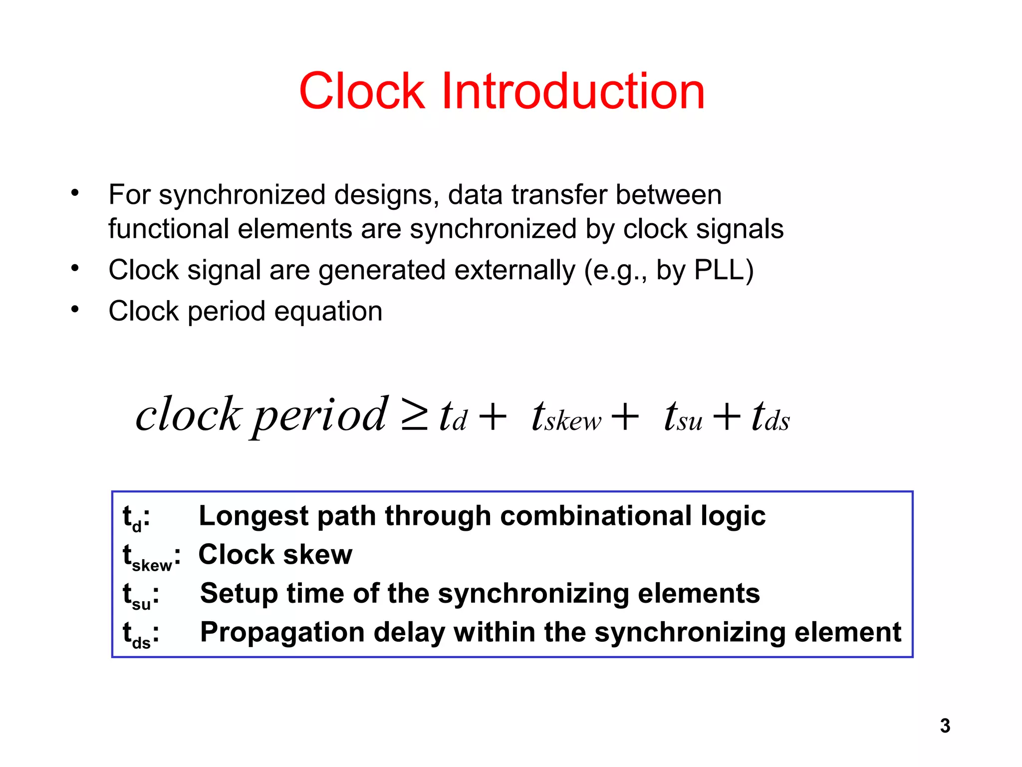
Need for clock signals in synchronized designs; clock period determined by various time factors affecting design.
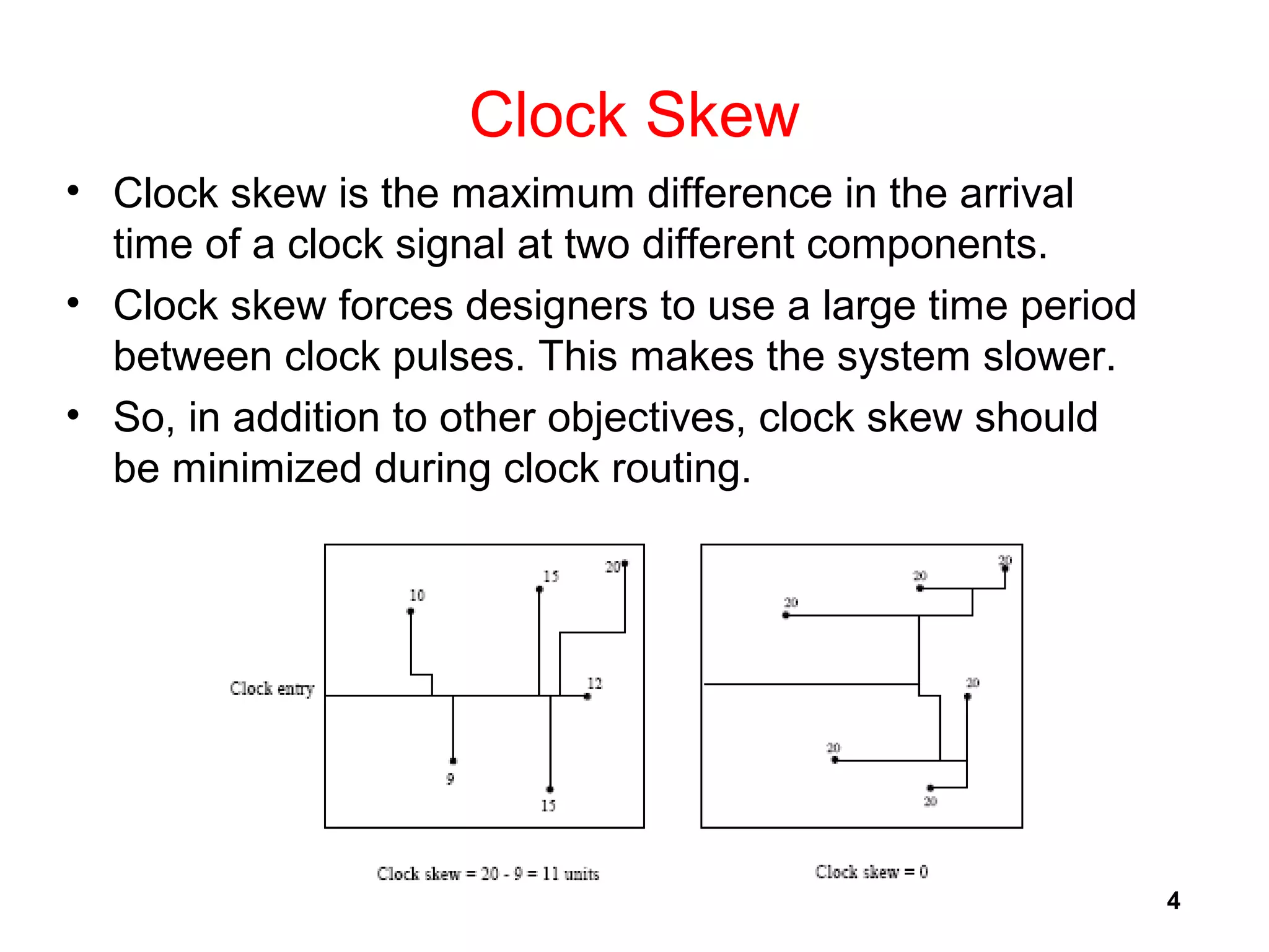
Definition of clock skew; its impact on system performance; emphasis on minimizing skew in clock routing.
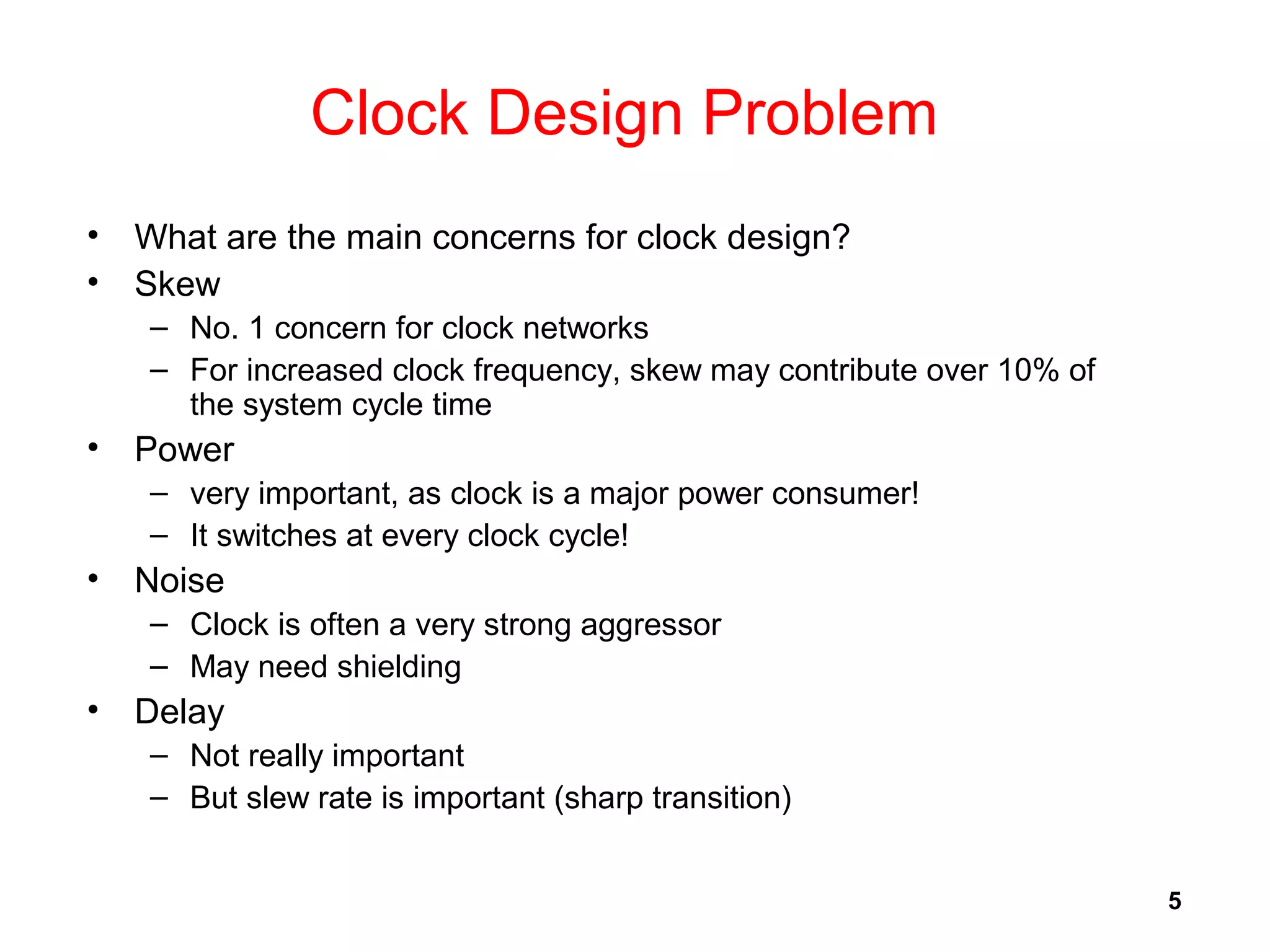
Critical considerations in clock design including skew, power, noise, and delay, particularly for high frequencies.
Minimization objectives in clock routing: skew, delay, total wire length, and noise.
Global nature of clock nets; importance of routing strategies, buffer insertion, and wire sizing.
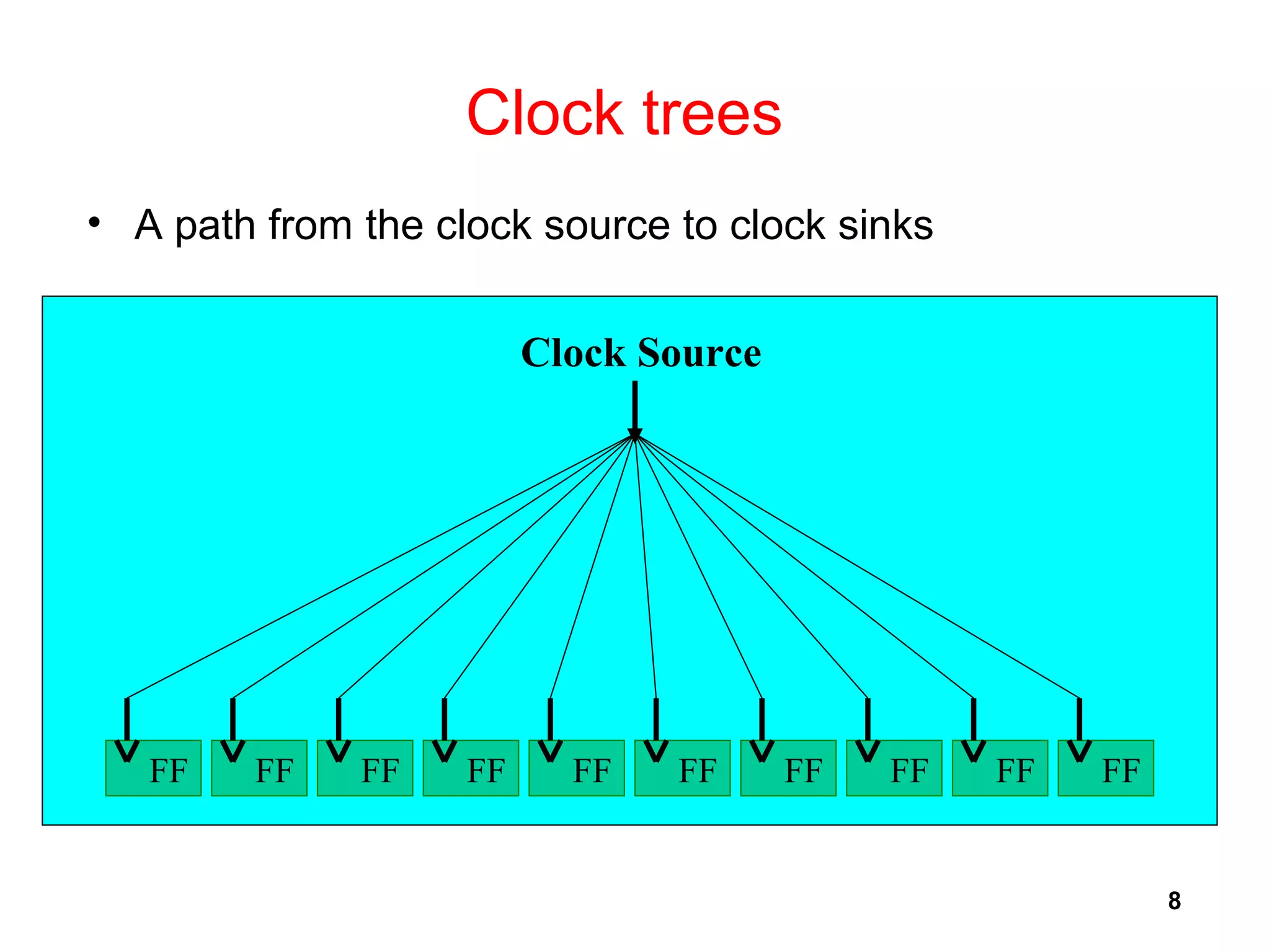
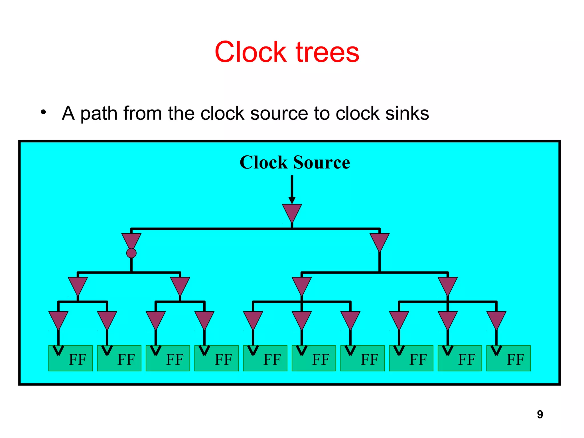
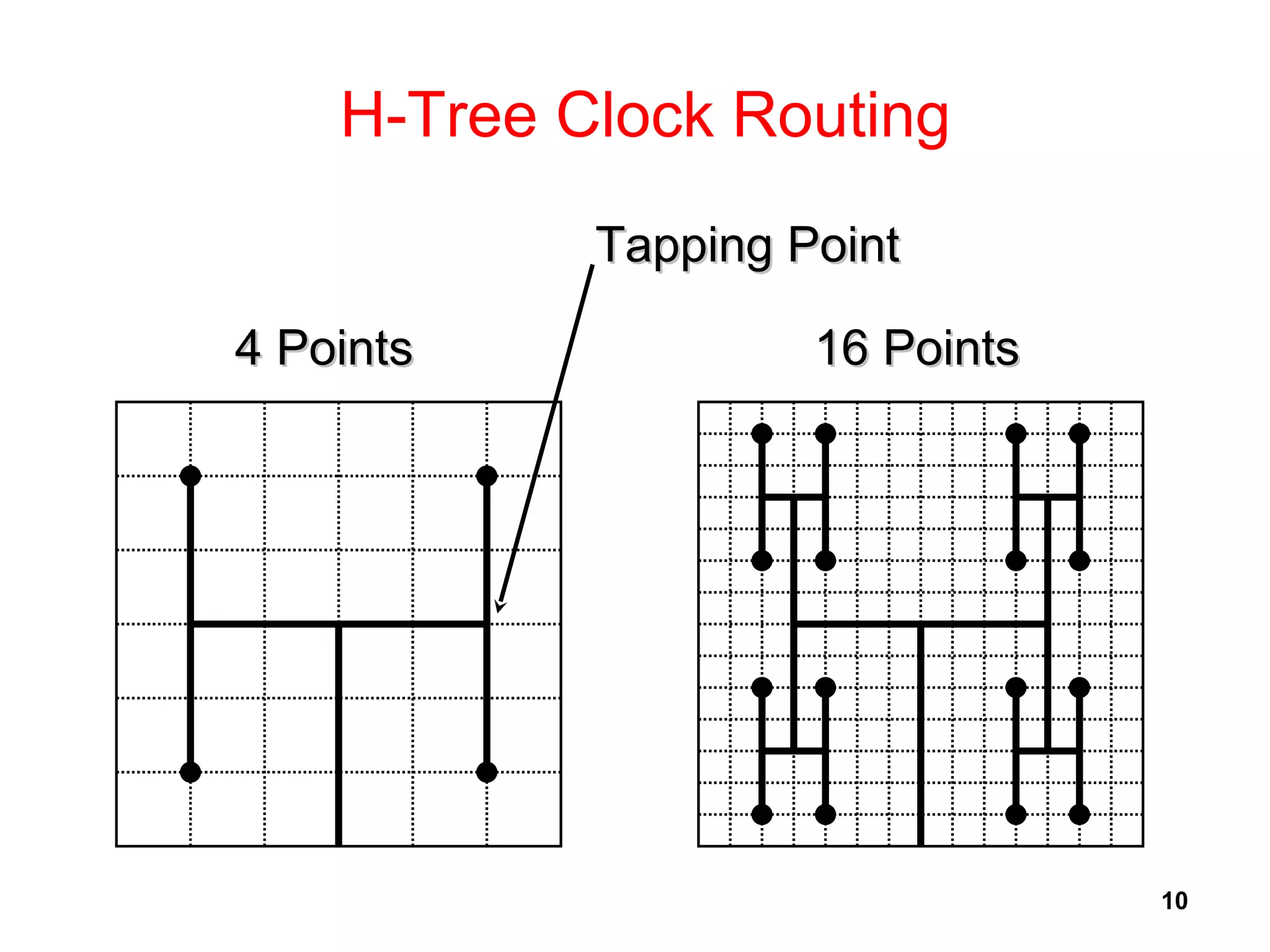
Basic structure of clock trees connecting a source to clock sinks, highlighting the layout concept.
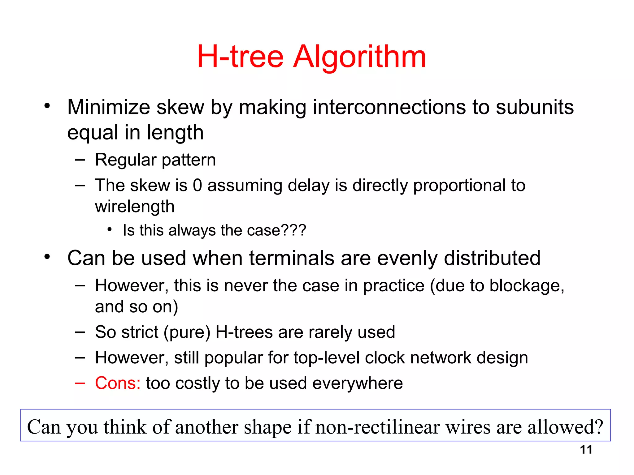
Minimizing clock skew with an H-tree structure; challenges in practical application due to non-ideal distributions.
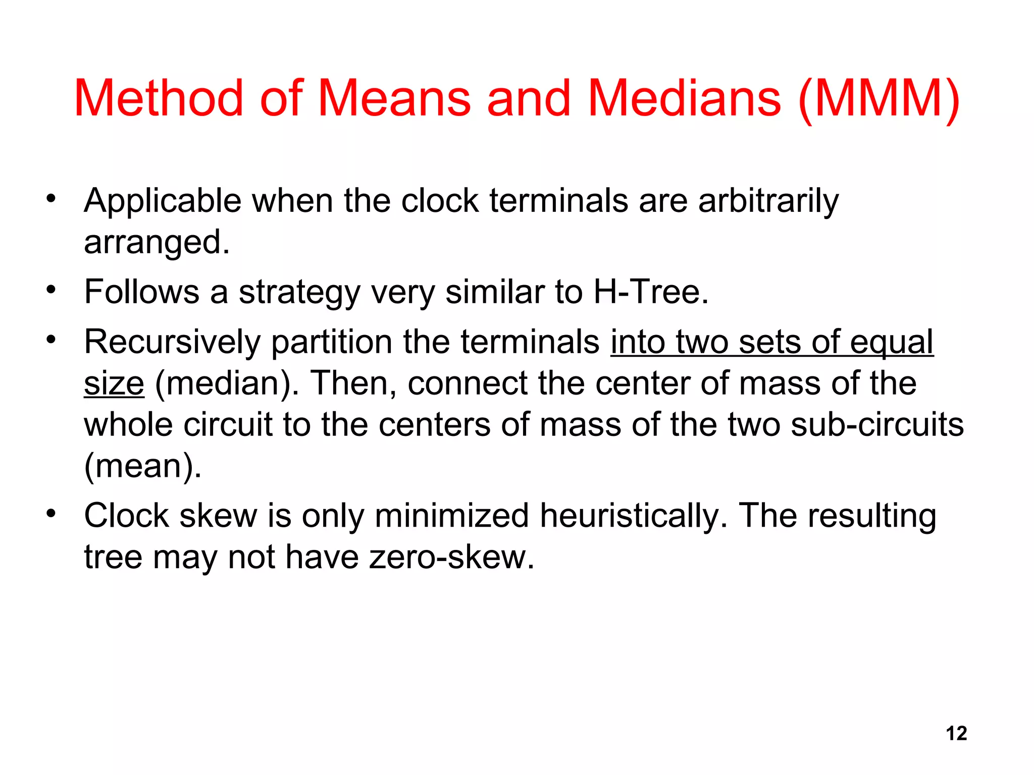
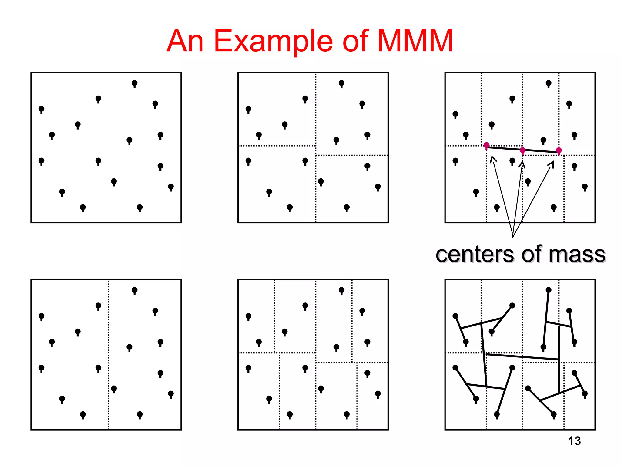
Heuristic strategy using median for terminal arrangement in clock routing to minimize skew.
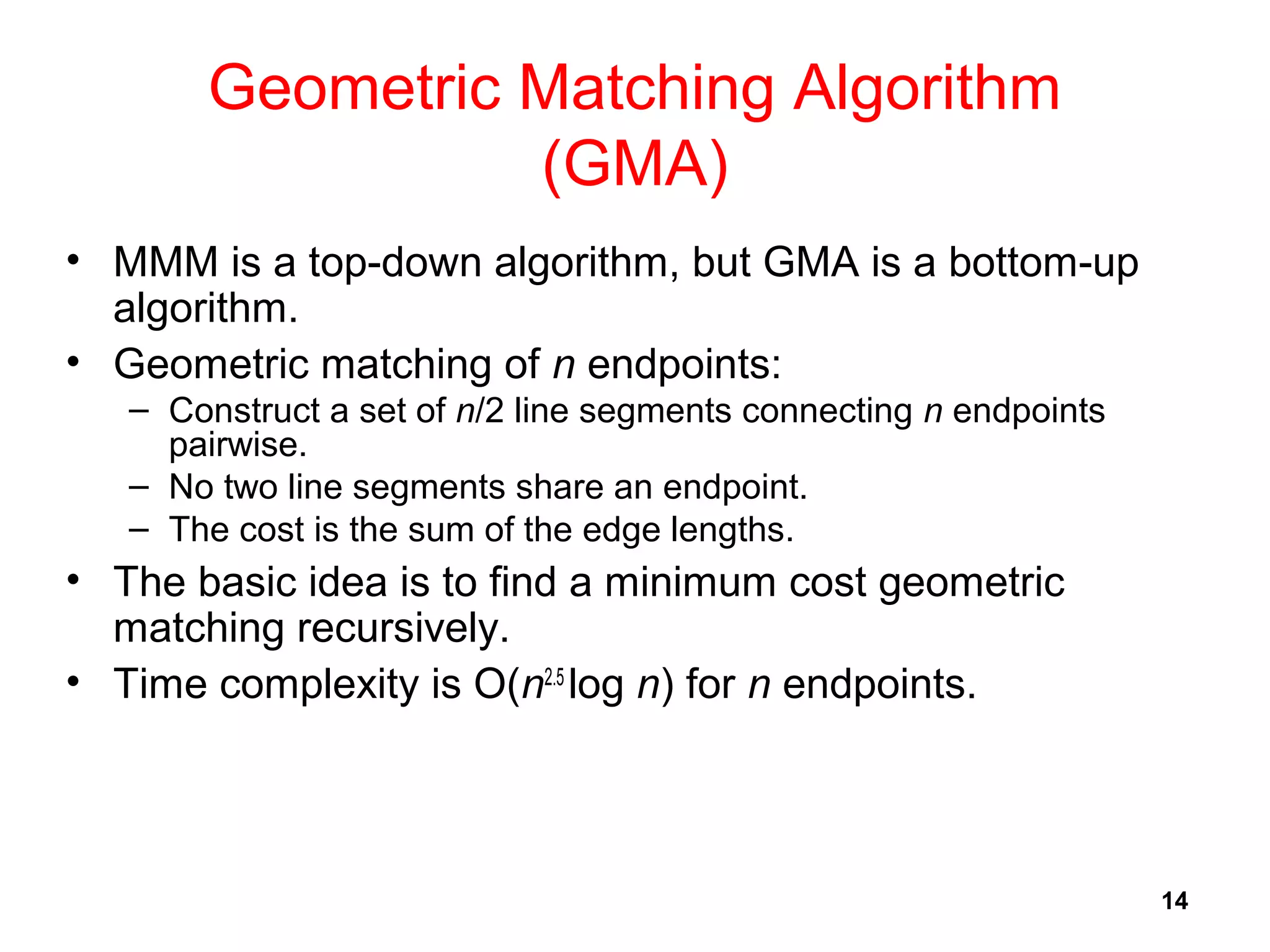
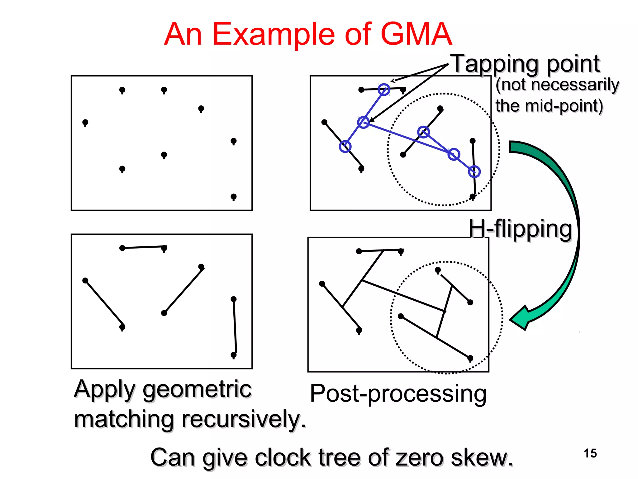
Bottom-up algorithm approach for minimizing cost through geometric pairing in clock routing.
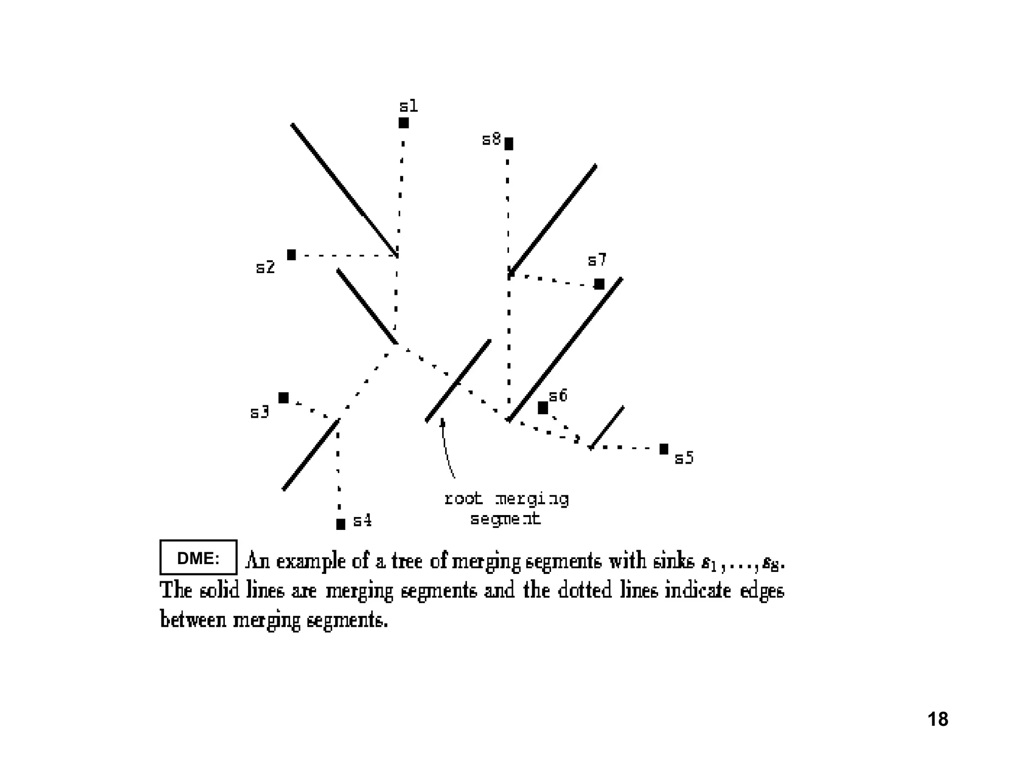
Detailed method for achieving zero skew in clock designs; mention of further research challenges.
DME strategy emphasizes late merging for minimal wire length; bottom-up and top-down phases outlined.
Advancements in clock skew scheduling and synthesis in response to increasing variability in designs.
Implementation of non-tree clock networks in high-performance processors; focus on links for skew reduction.
Goals of power distribution: current carrying, voltage stability, noise reduction, and layout efficiency.
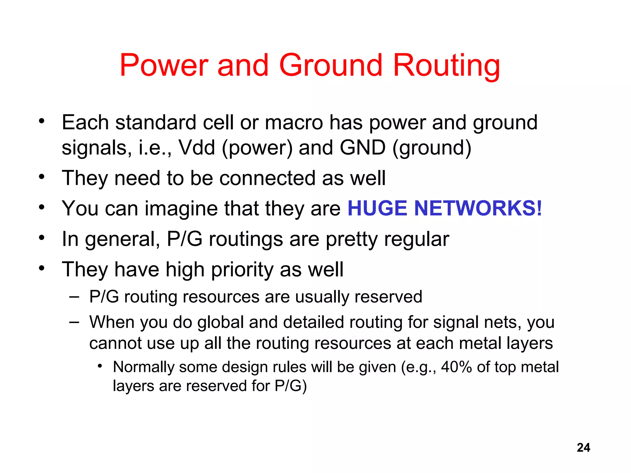
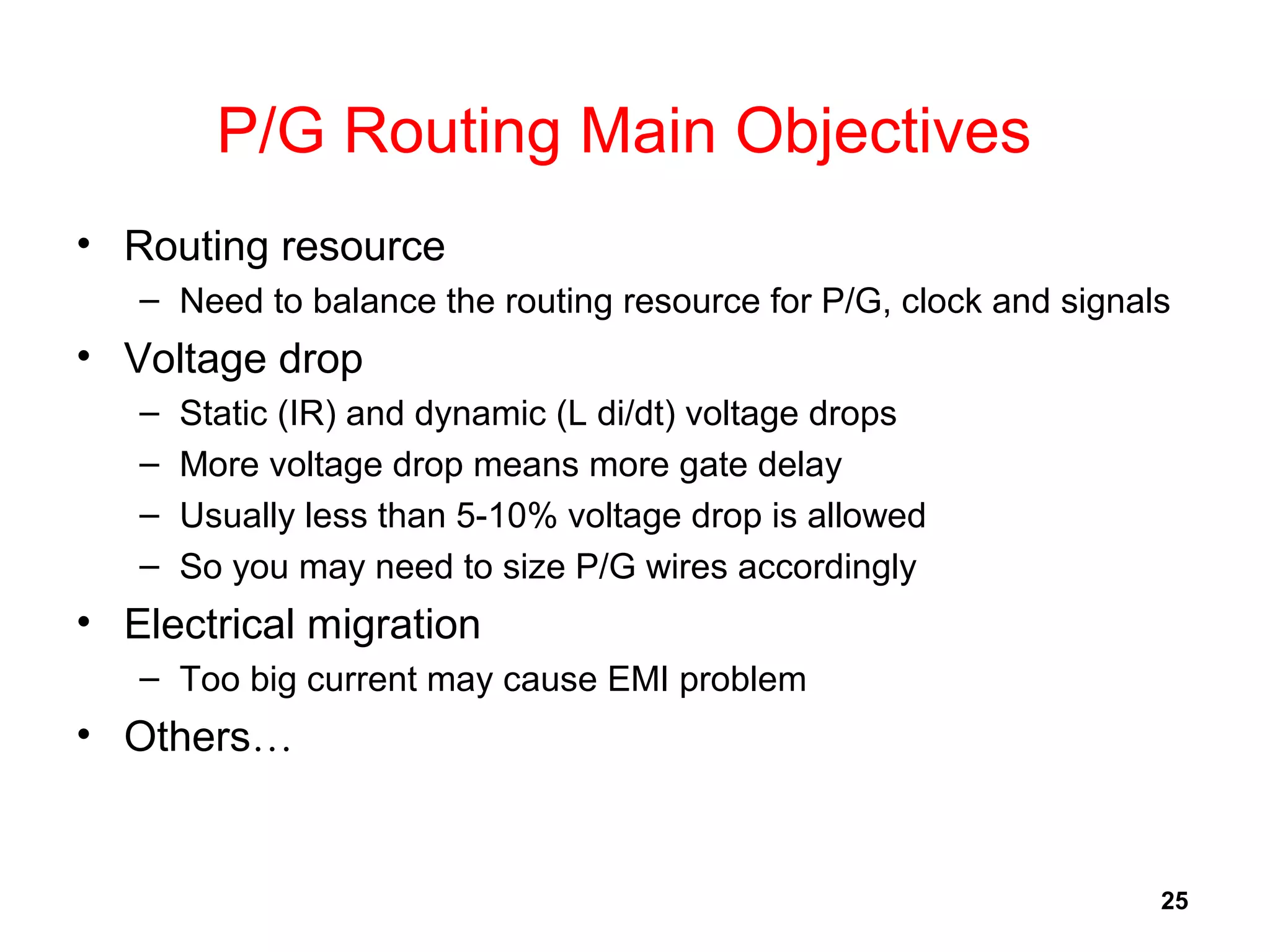
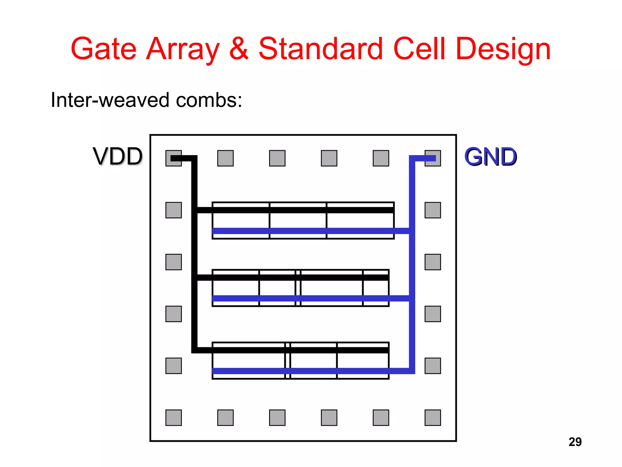
Focus on power/ground (P/G) routing importance, regularities, priority, and design rules for resource allocation.
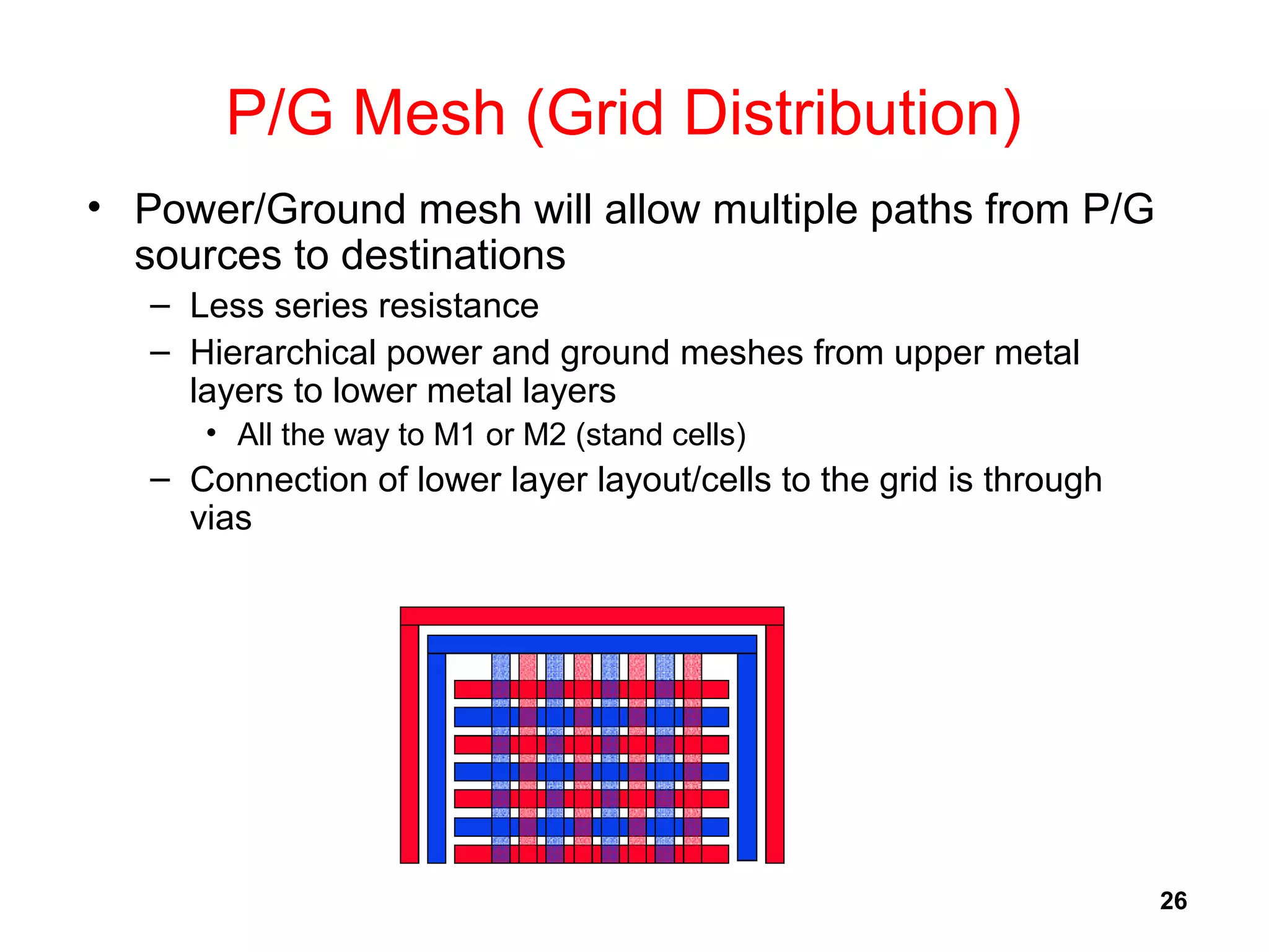
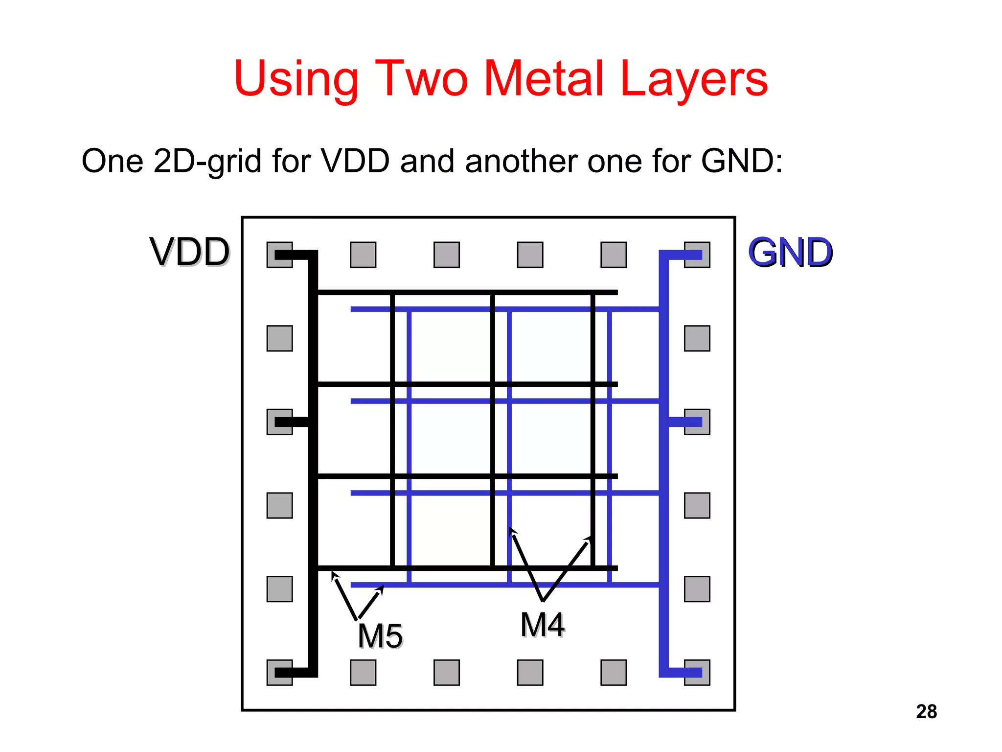
Mesh routing for reduced resistance and improved connections; hierarchical designs explained.
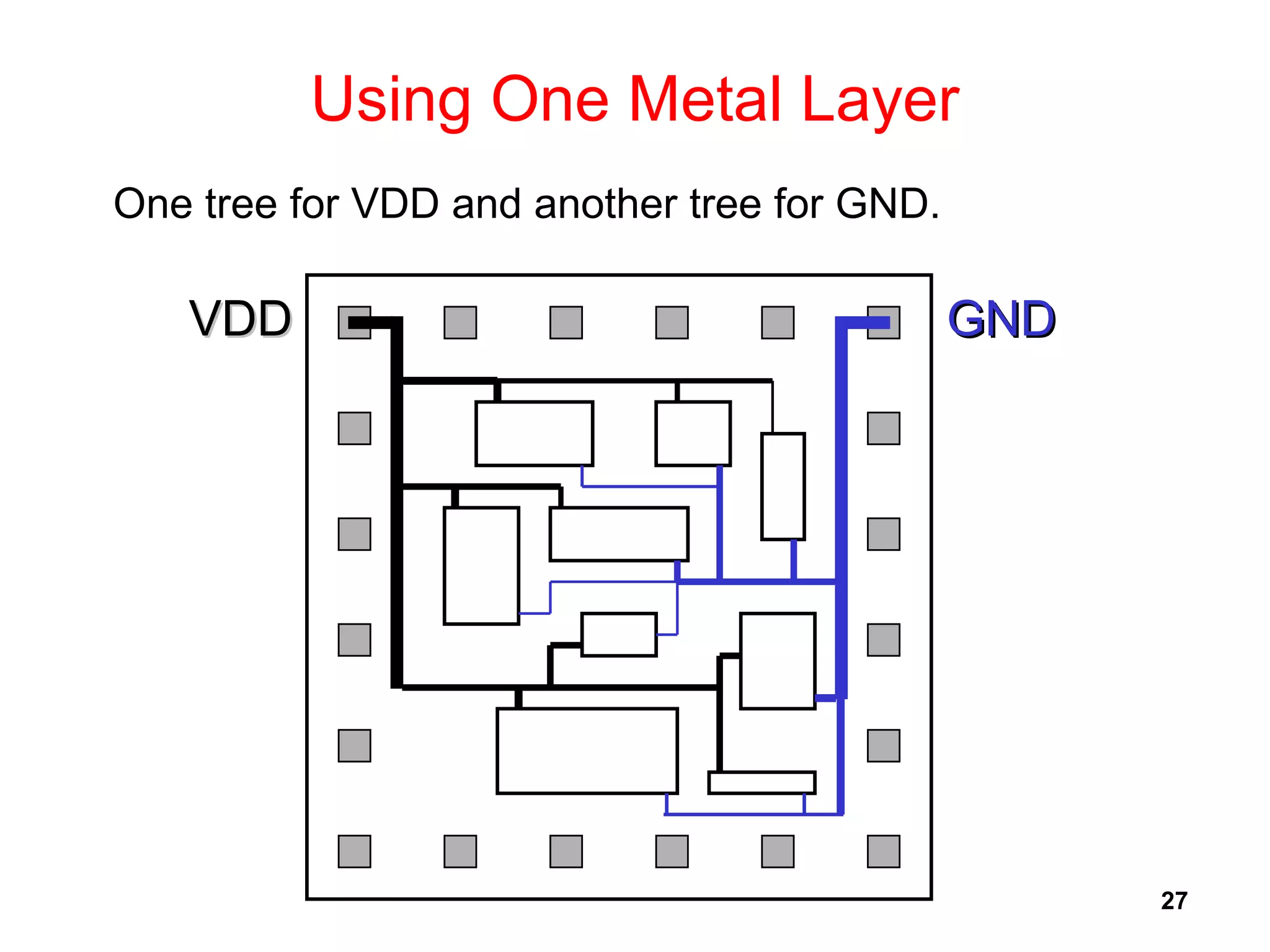
Design challenges with multiple metal layers for VDD and GND; implications for standard cell layout.
Modern practices in P/G I/O optimization, capacitor use, and complexities of voltage islands.