Downloaded 148 times
![[1] Karthick Murukesan, Narsimha Rao Mavilla, “Towards Fabrication of Low
Cost High Efficiency c-Si Solar Cells:Progress and Optimisation Using TCAD
Simulation Study” ,India, IEEE 2011.
[2] M. S. Bahrudin, S.F. Abdullah and I. Ahmad, “Statistical Modeling of Solar
Cell using Taguchi Method and TCAD Tool” ,Malaysia, IEEE 2012.
[3] Michael Duane, “The Role of TCAD in Compact Modelling ” , 3320 Scott
Blvd.,MS 1148,Santa Clara,CA.
[4] Sentaurus tool User Guide https://solvnet.synopsys.com..
• Refrences](https://image.slidesharecdn.com/nmosdesignraj-140708221659-phpapp02/75/Nmos-design-using-synopsys-TCAD-tool-23-2048.jpg)


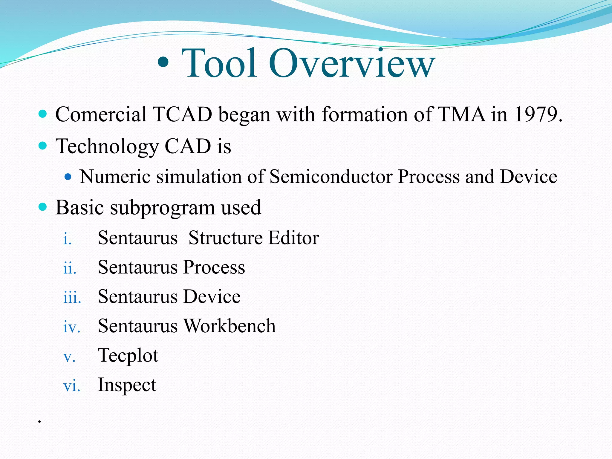
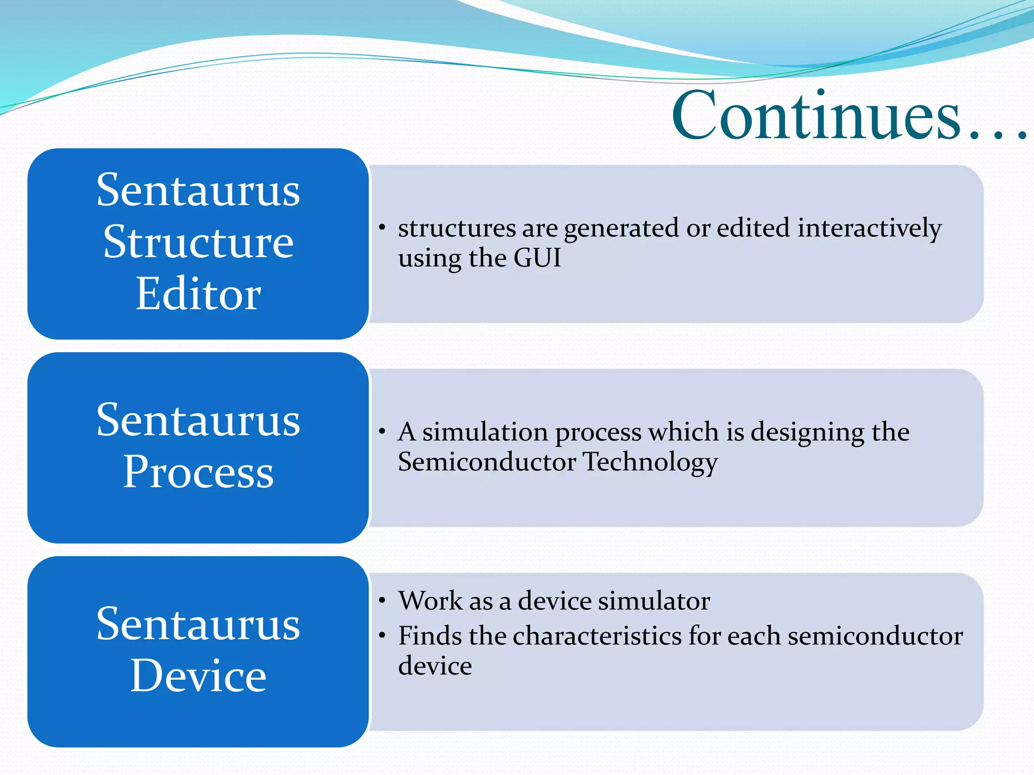
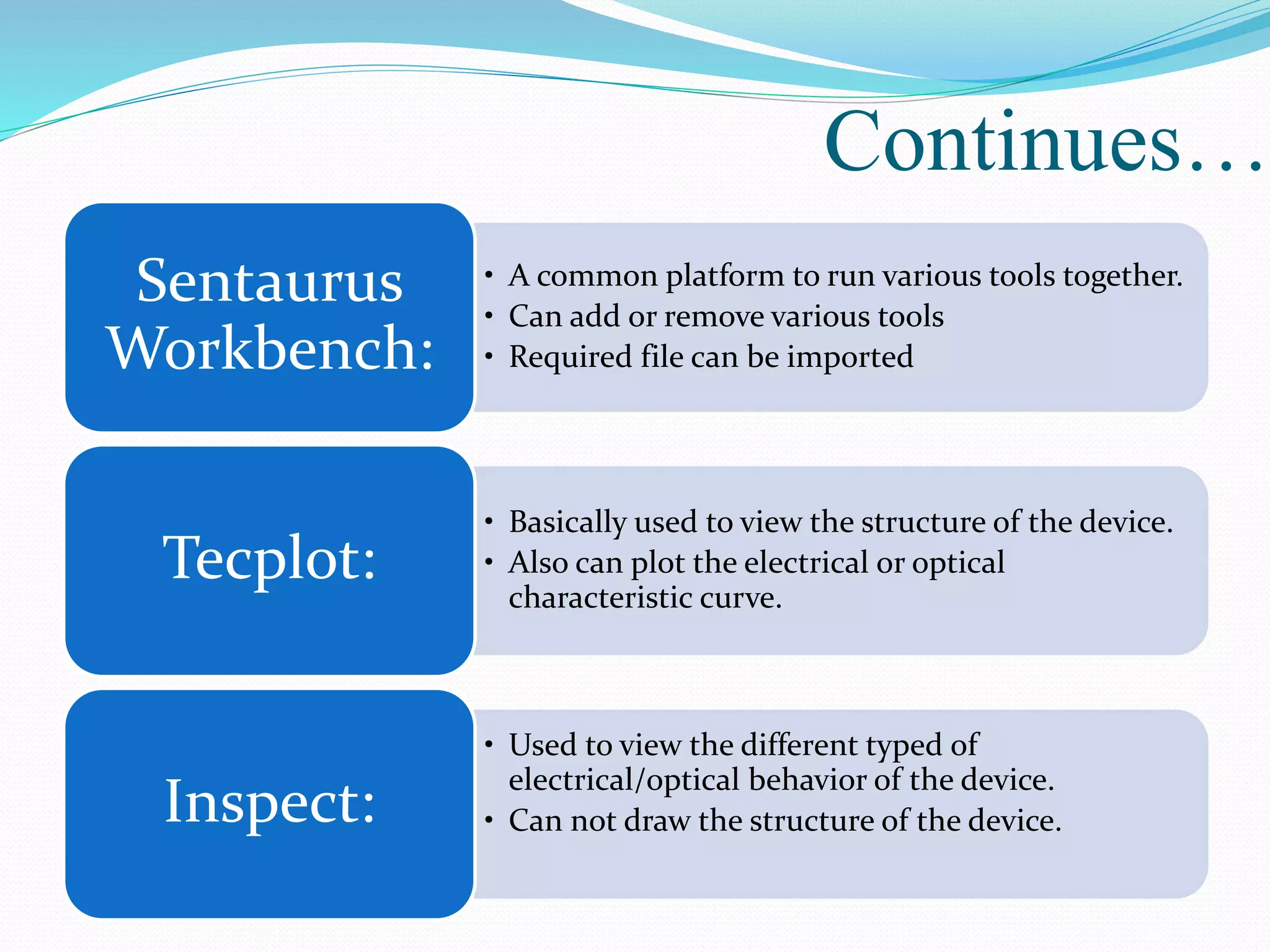
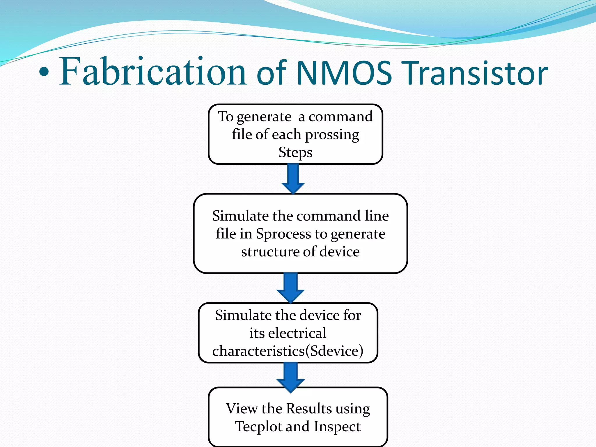
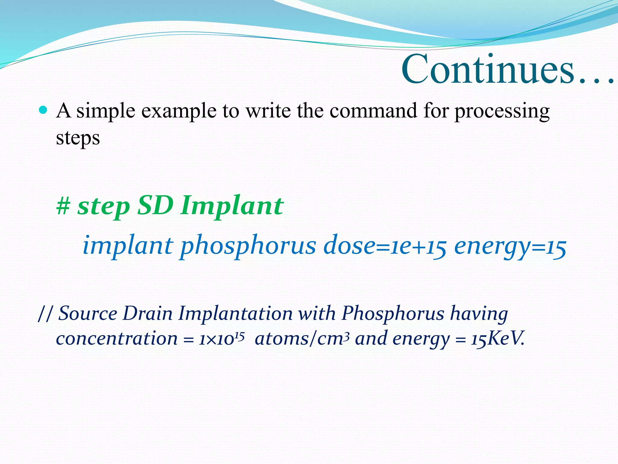
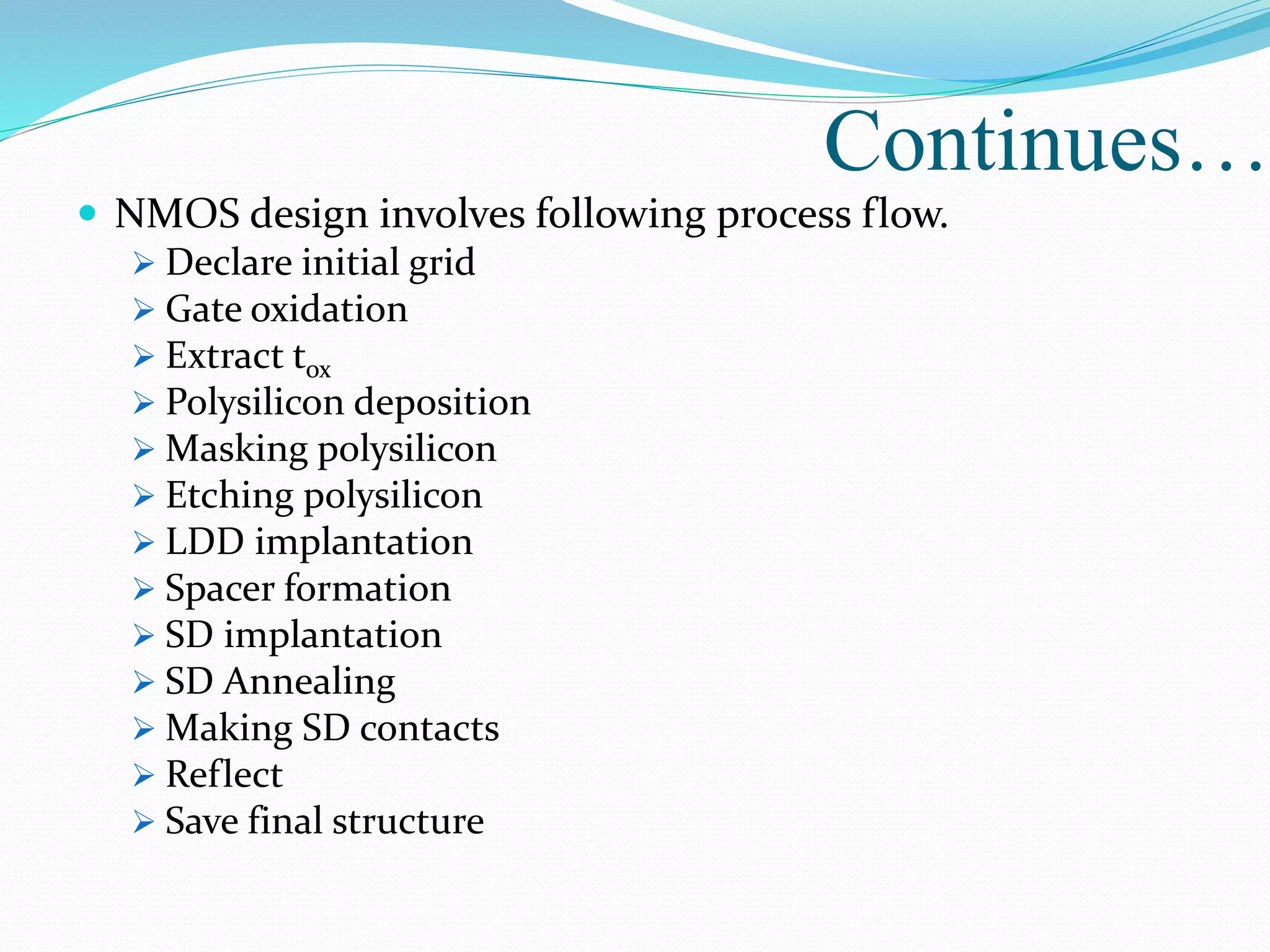
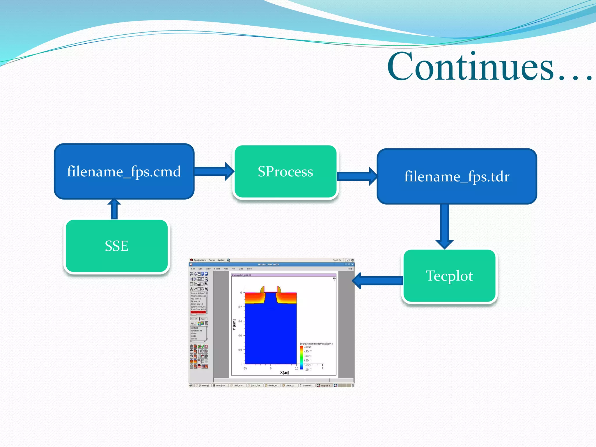
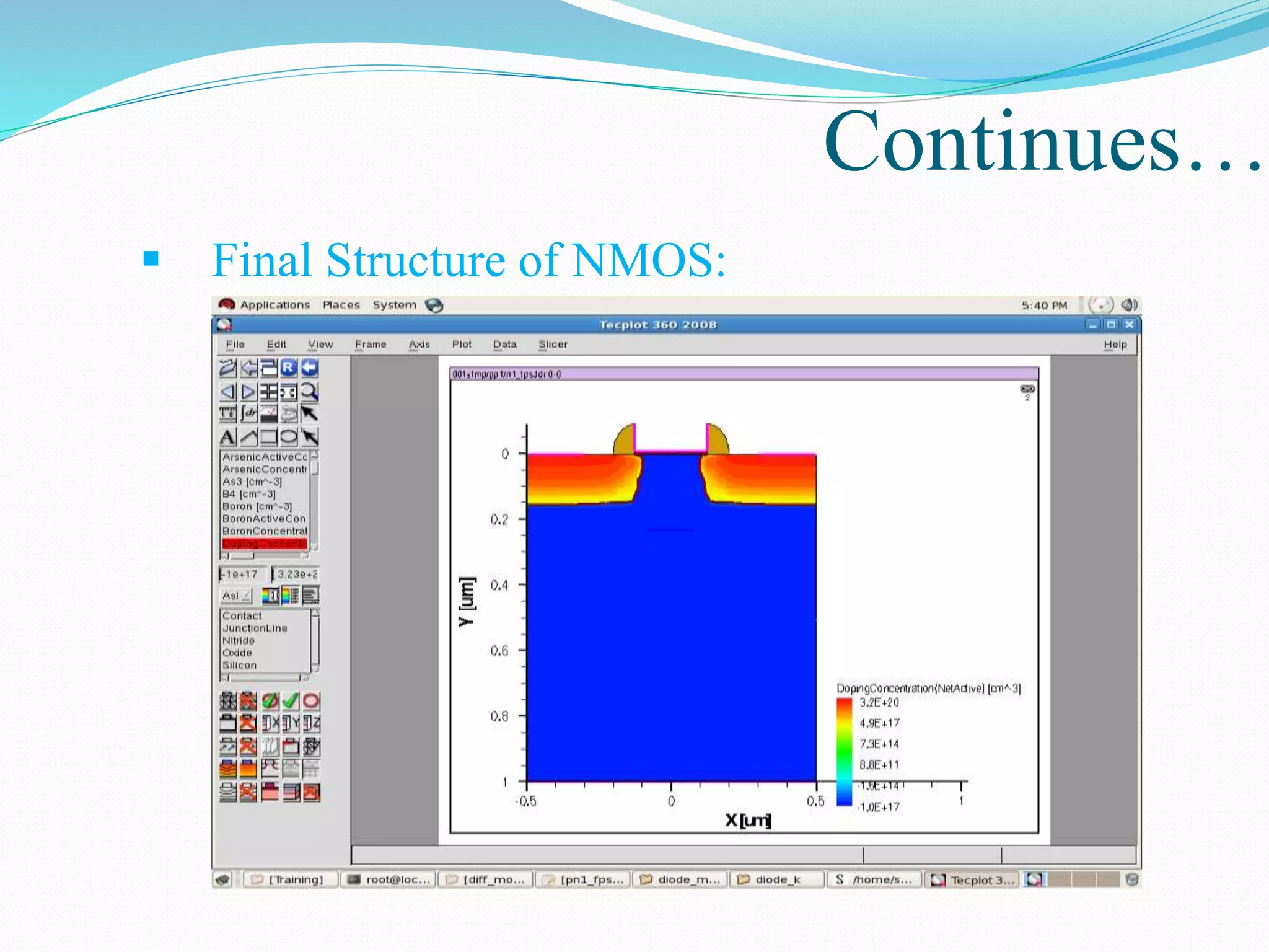
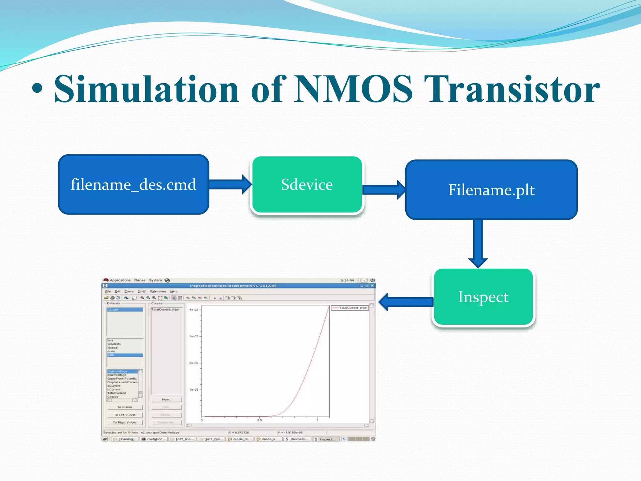
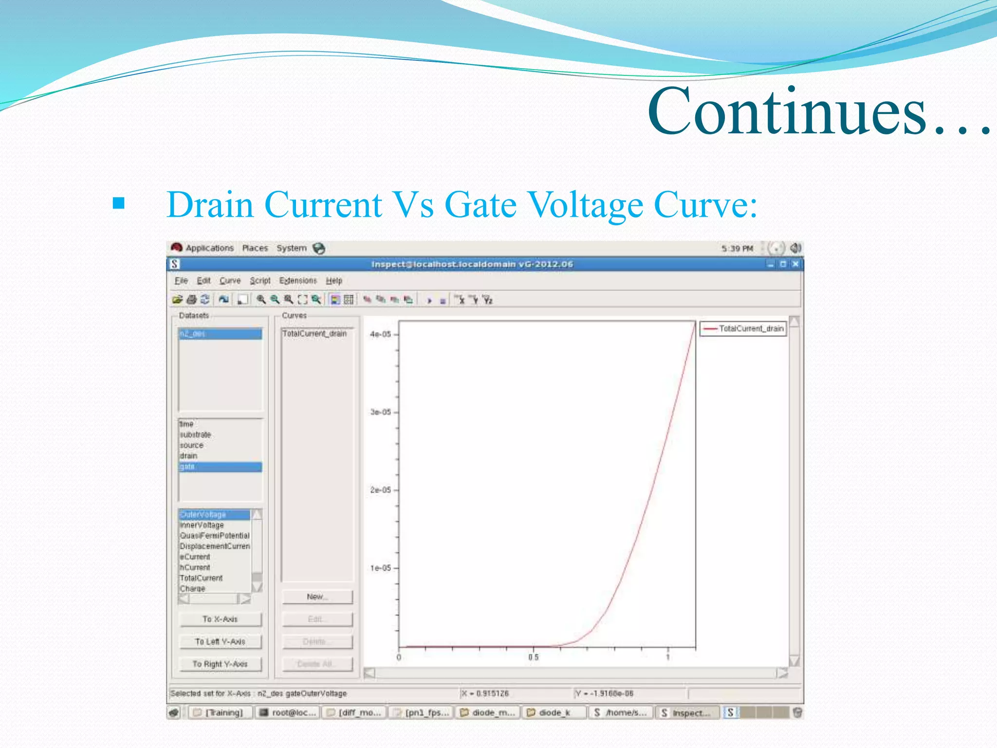
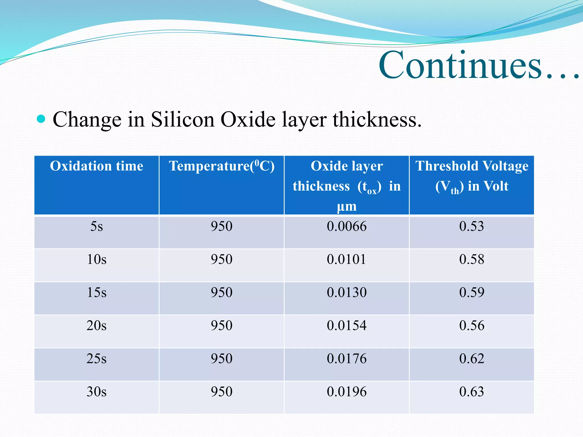
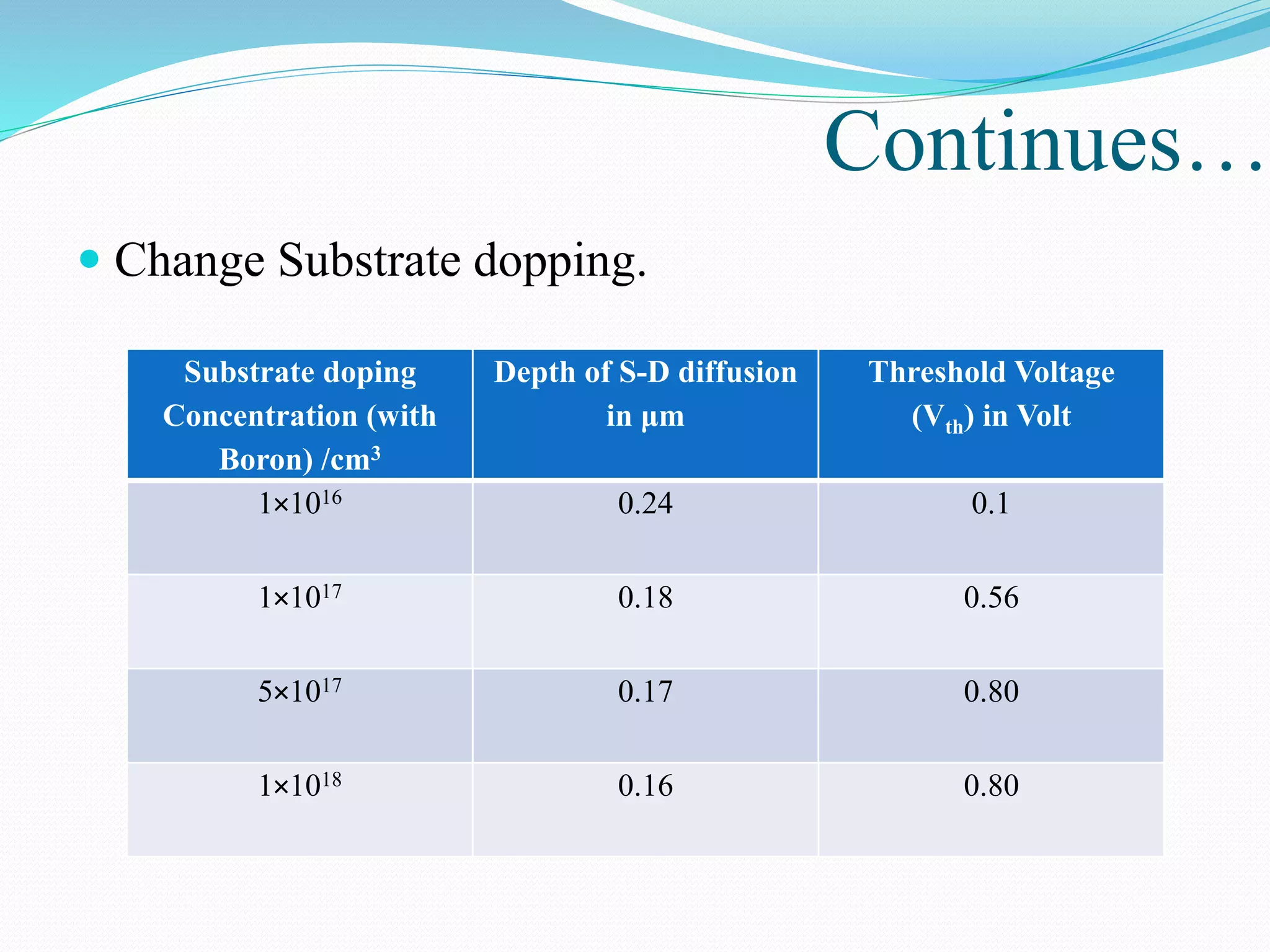
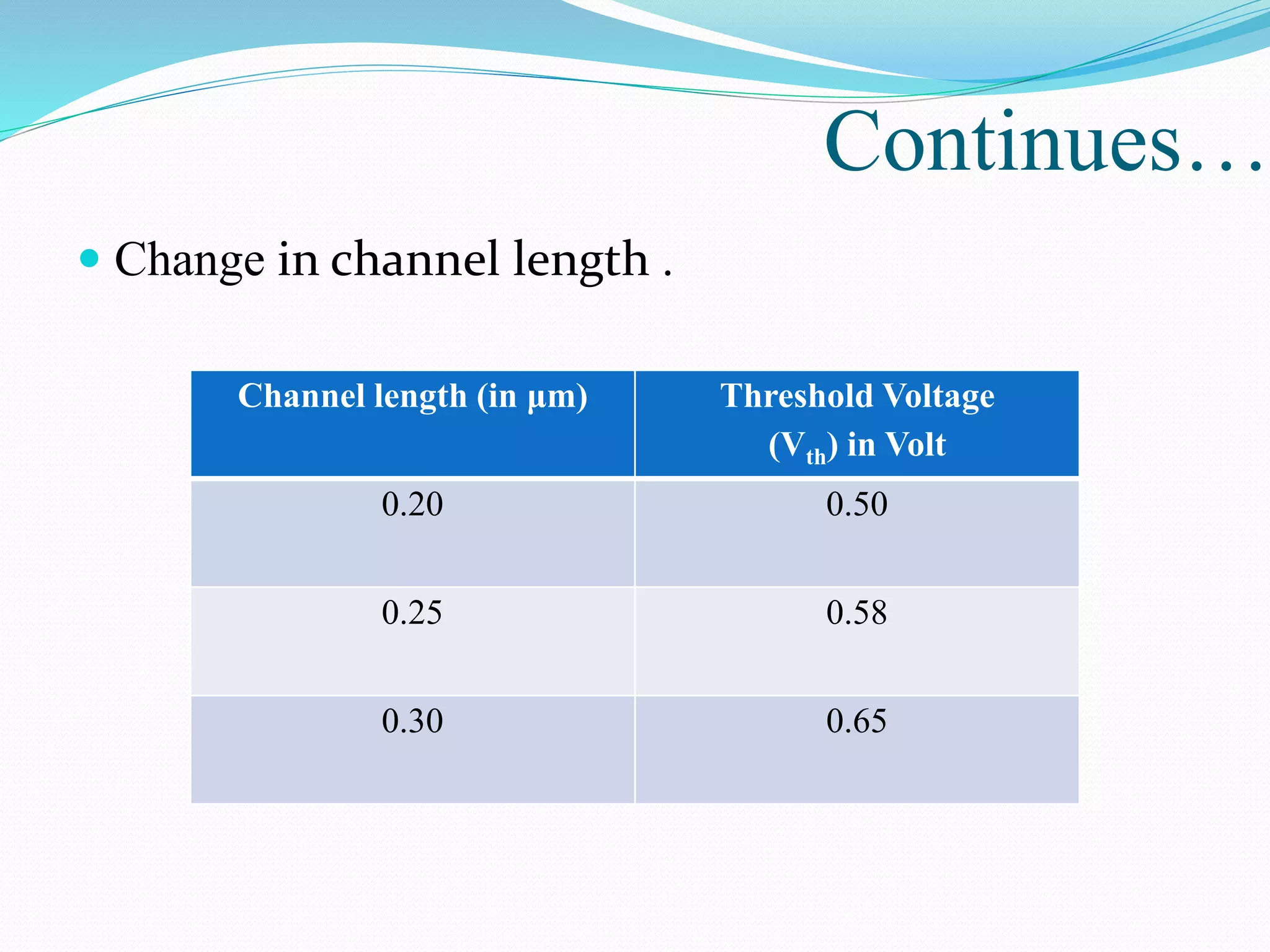
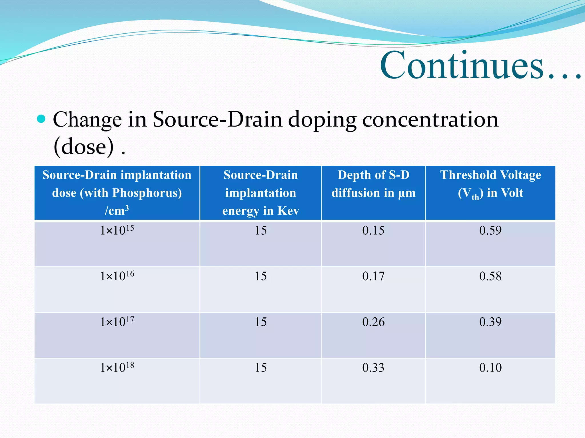
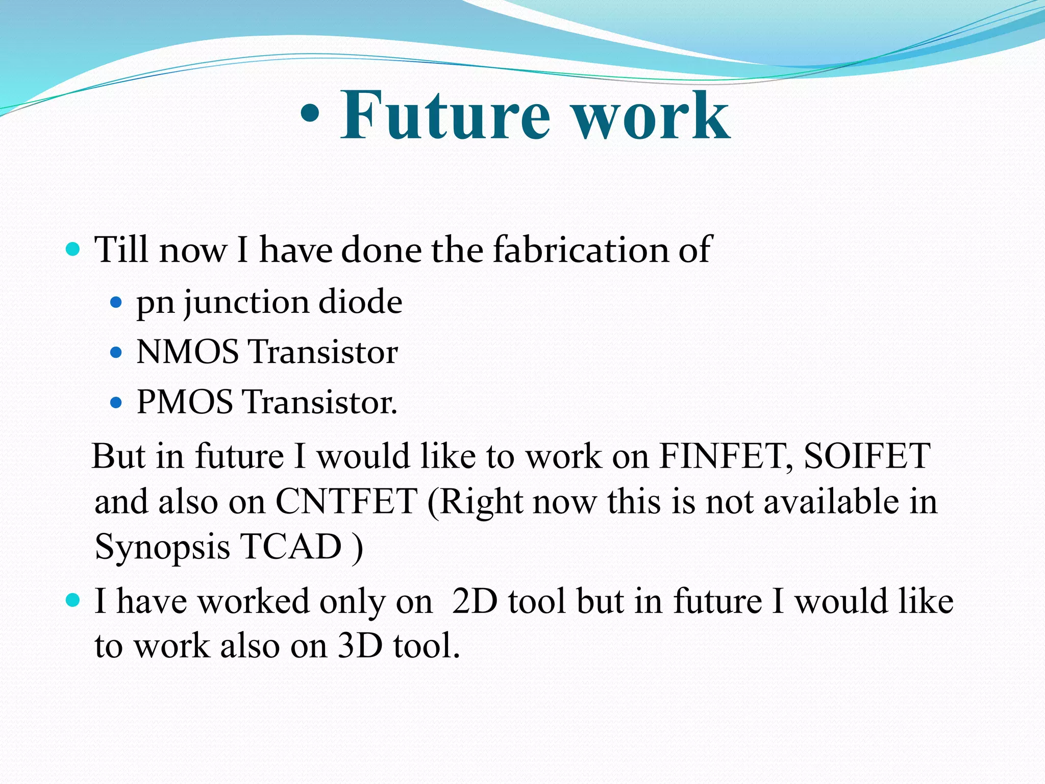
The document summarizes a presentation on simulating an NMOS transistor using TCAD tools. It introduces the topics covered, which include an overview of TCAD tools like Sentaurus Structure Editor, Process, Device, and Workbench. It then describes the fabrication process of the NMOS transistor through simulations in Sentaurus Process. The device is then simulated in Sentaurus Device to obtain electrical characteristics. Analytical results are discussed by varying device parameters. Future work aims to simulate more advanced devices like FinFETs and CNTFETs using 3D tools.