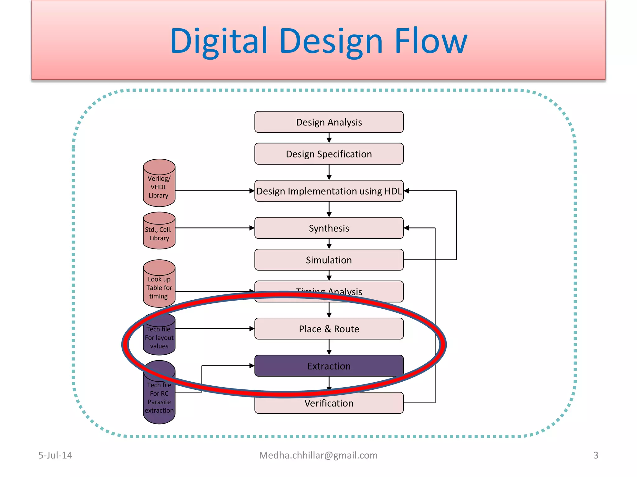
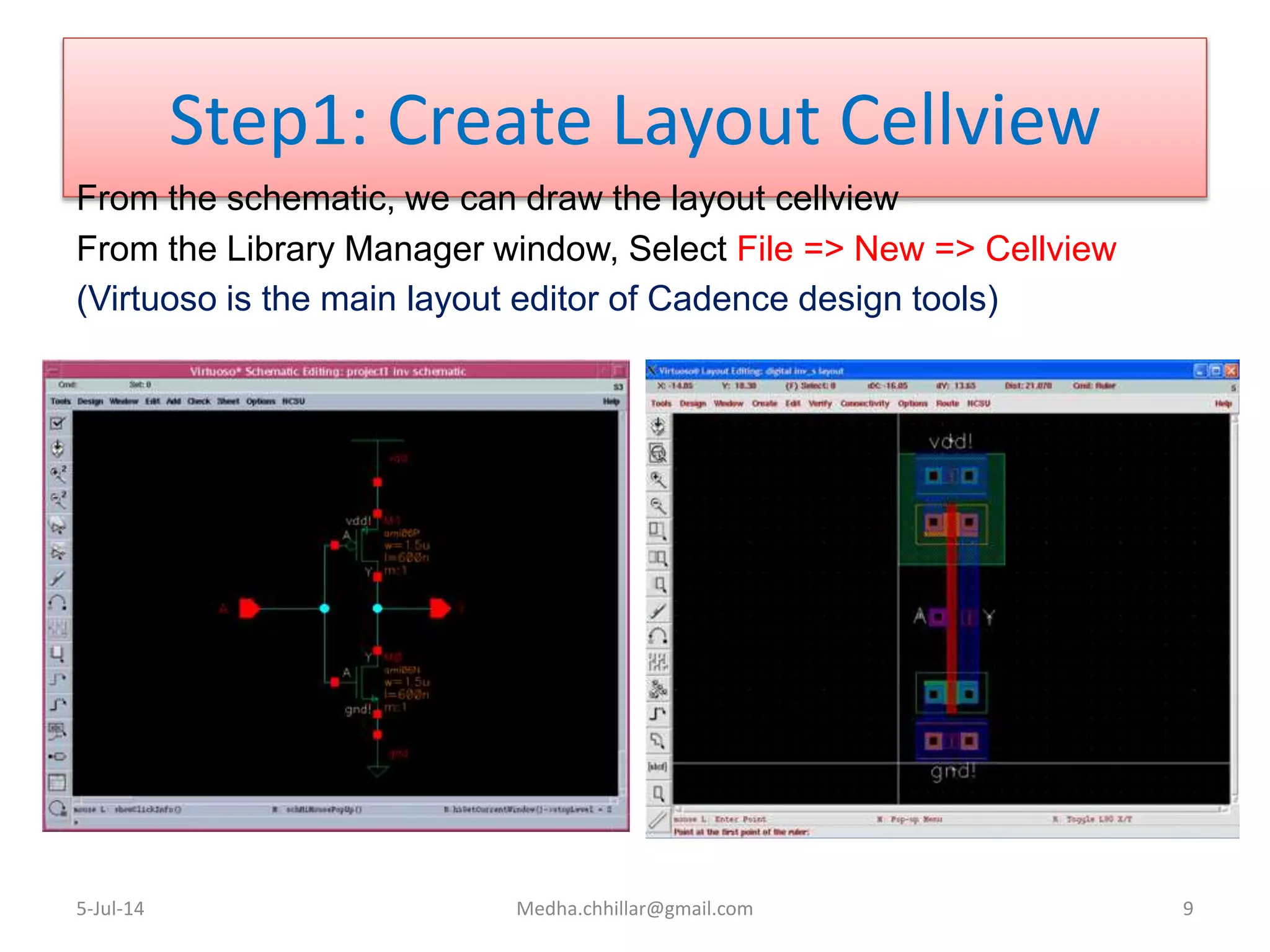
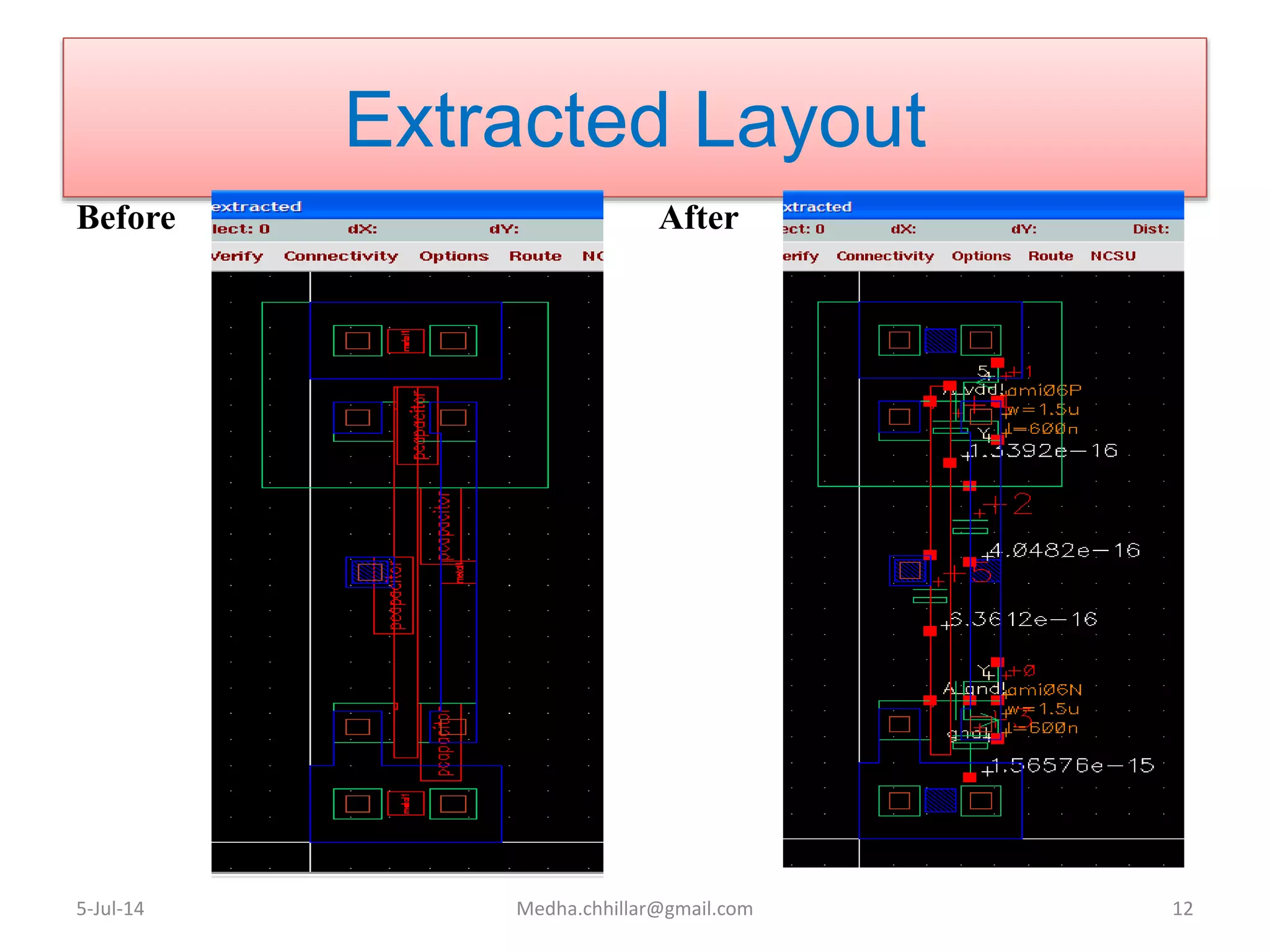
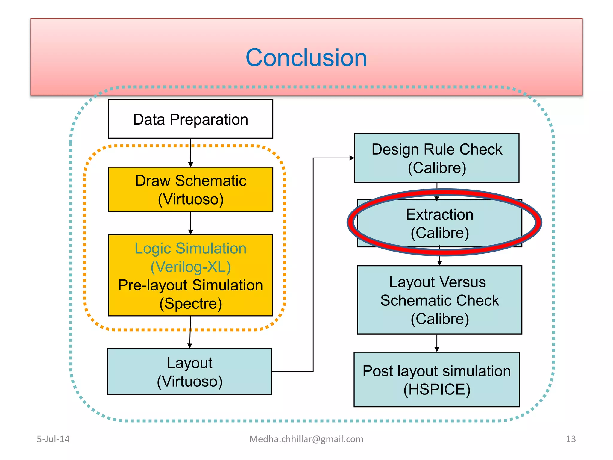
LAYOUT EXTRACTION
AGENDA
• Digital Design Flow
• Basics of Layout
• About Layout Extractor
• Tools used
• Steps to Extract layout
5-Jul-14 Medha.chhillar@gmail.com 2
Digital Design Flow
5-Jul-14 Medha.chhillar@gmail.com 3
Design Analysis
Design Specification
Synthesis
Design Implementation using HDL
Simulation
Timing Analysis
Place & Route
Extraction
Verification
Verilog/
VHDL
Library
Std., Cell.
Library
Look up
Table for
timing
Tech file
For layout
values
Tech file
For RC
Parasite
extraction
Basics of Layout
• Layout can be very time consuming
– Design gates to fit together nicely
– Build a library of standard cells
– Must follow a technology rule
• Standard cell design methodology
– VDD and GND should abut (standard height)
– Adjacent gates should satisfy design rules
– nMOS at bottom and pMOS at top
– All gates include well and substrate contacts
5-Jul-14 Medha.chhillar@gmail.com 4
What Are Layout Extractors??
• Once the layout is made, there always is parasitic
capacitances and resistances associated with the
design.
• This is because of the compact layouts to make the
chips smaller. More you make compact layout more
will it introduce these parasitic components.
• These interferes in the functioning and performance of
the circuit in terms of timing, speed and power
consumption.
5-Jul-14 Medha.chhillar@gmail.com 5
Contd…
• Examine the inter-relationship of mask layers
to infer the existence of transistors and other
components
• Related to Design Rule Checkers
– Design-rule Verification
• Some form of layout extraction is usually done
to create data for back annotation
5-Jul-14 Medha.chhillar@gmail.com 6
Tools used for Extraction
• FastCap, FastHenry
• Star-RCXT
• QRC
• Calibre xACT3D
etc…
5-Jul-14 Medha.chhillar@gmail.com 7
Steps to Extract a Layout
• Create Layout Cellview
• Design Rule Checking
• Layout Parameter Extraction
• Layout vs. Schematic Comparison
5-Jul-14
Courtesy:http://www.egr.msu.edu/classes/ece410/mason/files/TutorialB.pdf
8
Step1: Create Layout Cellview
From the schematic, we can draw the layout cellview
From the Library Manager window, Select File => New => Cellview
(Virtuoso is the main layout editor of Cadence design tools)
5-Jul-14 Medha.chhillar@gmail.com 9
Step2:Design Rule Checking
• After you have finished your layout, an automatic program will check
each and every polygon in your design against these design rules
and report violations. This process is called Design Rule Checking
(DRC) and MUST be done for every layout to ensure it will function
properly when fabricated.
• After the DRC is complete, the bottom line in the CIW(Command
Interpreter Window) will show “# Total errors found”
• The DRC will be successful when you see the results saying “0 Total
errors found”
5-Jul-14 Medha.chhillar@gmail.com 10
Step3: Layout Parameter
Extraction
• mask layout contains only physical data
• Extraction process identifies the devices from the layout and
generates a SPICE-like netlist and other files necessary to complete
the design process
• In the Virtuoso Layout Editing window select Verify => Extract
5-Jul-14 Medha.chhillar@gmail.com 11
Extracted Layout
Before After
5-Jul-14 Medha.chhillar@gmail.com 12
Conclusion
5-Jul-14 Medha.chhillar@gmail.com 13
Data Preparation
Draw Schematic
(Virtuoso)
Logic Simulation
(Verilog-XL)
Pre-layout Simulation
(Spectre)
Layout
(Virtuoso)
Design Rule Check
(Calibre)
Layout Versus
Schematic Check
(Calibre)
Extraction
(Calibre)
Post layout simulation
(HSPICE)
THANK YOU
5-Jul-14 Medha.chhillar@gmail.com 14

CAD: Layout Extraction

  • 1.
  • 2.
    AGENDA • Digital DesignFlow • Basics of Layout • About Layout Extractor • Tools used • Steps to Extract layout 5-Jul-14 Medha.chhillar@gmail.com 2
  • 3.
    Digital Design Flow 5-Jul-14Medha.chhillar@gmail.com 3 Design Analysis Design Specification Synthesis Design Implementation using HDL Simulation Timing Analysis Place & Route Extraction Verification Verilog/ VHDL Library Std., Cell. Library Look up Table for timing Tech file For layout values Tech file For RC Parasite extraction
  • 4.
    Basics of Layout •Layout can be very time consuming – Design gates to fit together nicely – Build a library of standard cells – Must follow a technology rule • Standard cell design methodology – VDD and GND should abut (standard height) – Adjacent gates should satisfy design rules – nMOS at bottom and pMOS at top – All gates include well and substrate contacts 5-Jul-14 Medha.chhillar@gmail.com 4
  • 5.
    What Are LayoutExtractors?? • Once the layout is made, there always is parasitic capacitances and resistances associated with the design. • This is because of the compact layouts to make the chips smaller. More you make compact layout more will it introduce these parasitic components. • These interferes in the functioning and performance of the circuit in terms of timing, speed and power consumption. 5-Jul-14 Medha.chhillar@gmail.com 5
  • 6.
    Contd… • Examine theinter-relationship of mask layers to infer the existence of transistors and other components • Related to Design Rule Checkers – Design-rule Verification • Some form of layout extraction is usually done to create data for back annotation 5-Jul-14 Medha.chhillar@gmail.com 6
  • 7.
    Tools used forExtraction • FastCap, FastHenry • Star-RCXT • QRC • Calibre xACT3D etc… 5-Jul-14 Medha.chhillar@gmail.com 7
  • 8.
    Steps to Extracta Layout • Create Layout Cellview • Design Rule Checking • Layout Parameter Extraction • Layout vs. Schematic Comparison 5-Jul-14 Courtesy:http://www.egr.msu.edu/classes/ece410/mason/files/TutorialB.pdf 8
  • 9.
    Step1: Create LayoutCellview From the schematic, we can draw the layout cellview From the Library Manager window, Select File => New => Cellview (Virtuoso is the main layout editor of Cadence design tools) 5-Jul-14 Medha.chhillar@gmail.com 9
  • 10.
    Step2:Design Rule Checking •After you have finished your layout, an automatic program will check each and every polygon in your design against these design rules and report violations. This process is called Design Rule Checking (DRC) and MUST be done for every layout to ensure it will function properly when fabricated. • After the DRC is complete, the bottom line in the CIW(Command Interpreter Window) will show “# Total errors found” • The DRC will be successful when you see the results saying “0 Total errors found” 5-Jul-14 Medha.chhillar@gmail.com 10
  • 11.
    Step3: Layout Parameter Extraction •mask layout contains only physical data • Extraction process identifies the devices from the layout and generates a SPICE-like netlist and other files necessary to complete the design process • In the Virtuoso Layout Editing window select Verify => Extract 5-Jul-14 Medha.chhillar@gmail.com 11
  • 12.
    Extracted Layout Before After 5-Jul-14Medha.chhillar@gmail.com 12
  • 13.
    Conclusion 5-Jul-14 Medha.chhillar@gmail.com 13 DataPreparation Draw Schematic (Virtuoso) Logic Simulation (Verilog-XL) Pre-layout Simulation (Spectre) Layout (Virtuoso) Design Rule Check (Calibre) Layout Versus Schematic Check (Calibre) Extraction (Calibre) Post layout simulation (HSPICE)
  • 14.

Editor's Notes

  • #7 Back Annotation: Once a layout has been constructed and there is isomorphism between schematic n/w and layout n/w, one can correlate extracted capacitances from the layout with the schematic and perform simulation or timing analysis to verify performance. This is done by moving the capacitance that appears on a layout node to the corresponding schematic node while accounting for existing capacitance on the schematic node. For instance, the schematic may already have source-drain and gate load due to gates connected to the node and only routing capacitance is required to be added. This operation is called “Back-Annotation”.