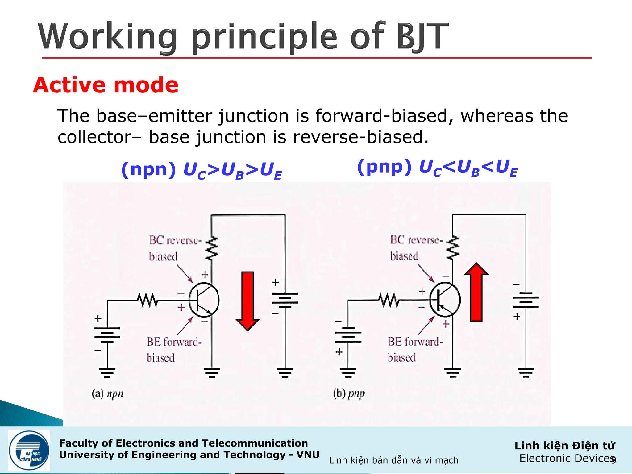
Faculty of Electronics and Telecommunication
University of Engineering and Technology - VNU
Linh kiện Điện tử
Electronic Devices
1) ELECTRONIC DEVICES, 9th edition, Thomas L. Floyd, Prentice Hall
2) Semiconductor Physics And Devices, 3rd ed. - J. Neamen
3) Robert L. Boylestad, Louis Nashelsky, Electronic Devices and Circuit Theory, 8th Edition,
Prentice Hall
4) Linh kiện bán dẫn và vi mạch, Hồ Văn Sung, NXB Giáo Dục, 2007
5) Giáo trình linh kiện điện tử, Trương Văn Tám, ĐH Cần Thơ, 2003.
References
Faculty of Electronics and Telecommunication
University of Engineering and Technology - VNU
Linh kiện Điện tử
Electronic Devices
2
 The bipolar junction transistor (BJT) is constructed with three doped
semiconductor regions separated by two pn junctions
 Regions are called emitter, base and collector
The invention of the
bipolar transistor in
1948 ushered in a
revolution in electronics
TS. Phạm Ngọc Thảo
Faculty of Electronics and Telecommunication
University of Engineering and Technology - VNU
Linh kiện Điện tử
Electronic Devices
3
TS. Phạm Ngọc Thảo
TRANSFER+ RESISTOR
→ TRANSISTOR
Vi = 200 mV  VL = 50V
 Increase x250 times
AMPLIFIER (KHUẾCH ĐẠI)
Faculty of Electronics and Telecommunication
University of Engineering and Technology - VNU
Linh kiện Điện tử
Electronic Devices
4
General-purpose/
small-signal
Power transistors
and packages.
Multiple-
transistor
packages
TS. Phạm Ngọc Thảo
Faculty of Electronics and Telecommunication
University of Engineering and Technology - VNU
Linh kiện Điện tử
Electronic Devices
5
TS. Phạm Ngọc Thảo
Faculty of Electronics and Telecommunication
University of Engineering and Technology - VNU
Linh kiện Điện tử
Electronic Devices
6
pnp npn
Common-Base
CB Configuration
Common-Collector
CC Configuration
Common-Emitter
CE Configuration
TS. Phạm Ngọc Thảo
Input
signal
Output
signal
Input
signal
Input
signal
Input
signal
Input
signal
Input
signal
Output
signal
Output
signal
Output
signal
Output
signal
Output
signal
Faculty of Electronics and Telecommunication
University of Engineering and Technology - VNU
Linh kiện Điện tử
Electronic Devices
7
The base–emitter and collector–base junctions of a transistor are
both reverse-biased.
The base–emitter and collector–base junctions are forward-biased.
The base–emitter junction is forward-biased, whereas the collector–
base junction is reverse-biased.
E
Faculty of Electronics and Telecommunication
University of Engineering and Technology - VNU
Linh kiện Điện tử
Electronic Devices
Linh kiện bán dẫn và vi mạch 8
Cutoff mode
The base–emitter and collector–base
junctions of a transistor are both
reverse-biased.
VCE ≈ VCC
Saturation mode
The base–emitter and collector–base
junctions of a transistor are both
forward-biased.
VCE ≈ 0
Faculty of Electronics and Telecommunication
University of Engineering and Technology - VNU
Linh kiện Điện tử
Electronic Devices
The base–emitter junction is forward-biased, whereas the
collector– base junction is reverse-biased.
Linh kiện bán dẫn và vi mạch 9
Active mode
(pnp) UC<UB<UE
(npn) UC>UB>UE
Faculty of Electronics and Telecommunication
University of Engineering and Technology - VNU
Linh kiện Điện tử
Electronic Devices
10
Active mode
The base–emitter junction is forward-biased, whereas the
collector– base junction is reverse-biased.
Faculty of Electronics and Telecommunication
University of Engineering and Technology - VNU
Linh kiện Điện tử
Electronic Devices
11
Chuyển tiếp P-N giữa cực Base và cực
Emitter được phân cực thuận bởi nguồn
VEE. Chuyển tiếp P-N giữa cực Base và
cực Collector được phân cực nghịch bởi
nguồn VCC.
Điện tử từ cực âm của nguồn VEE di
chuyển vào vùng Emitter qua vùng
Base, đáng lẽ trở về cực dương của
nguồn VEE nhưng vì:
+ Vì vùng Base rất hẹp với 2 vùng kia
+ Nguồn VCC >> VEE cho nên đa số điện
tử bị hấp dẫn về nó
Do đó, số lượng điện tử từ vùng Base
vào vùng thu tới cực dương của nguồn
VCC rất nhiều so với số lượng điện tử từ
vùng Base tới cực dương của nguồn VEE.
Sự dịch chuyển của điện tử tạo thành
dòng điện.
Dòng đi vào cực Base dgl dòng IB;
Dòng đi vào cực Collector dgl dòng IC;
Dòng đi vào cực Emitter dgl dòng IE.
n n
p
Faculty of Electronics and Telecommunication
University of Engineering and Technology - VNU
Linh kiện Điện tử
Electronic Devices
 Quy ước về chiều dòng điện là chiều từ cực dương đi qua
dây dẫn và các linh kiện tiêu thụ điện tới cực âm của
nguồn điện.
 Trong trường hợp npn, dòng dịch chuyển của các electron
tích điện âm dịch chuyển ngược chiều với chiều của dòng
điện
 npn còn được gọi là đèn (bóng) bán dẫn, BJT, ngược.
 Trong trường hợp pnp, dòng dịch chuyển của các lỗ trống
tích điện dương dịch chuyển cùng chiều chiều với chiều của
dòng điện
 pnp còn được gọi là đèn (bóng) bán dẫn, BJT, thuận.
12
Faculty of Electronics and Telecommunication
University of Engineering and Technology - VNU
Linh kiện Điện tử
Electronic Devices
13
We have
(1) IE = IB + IC
(2) IC =  IE where   0.95~0.99
Replace (2) into (1)
Take
The collector current is comprised of
two currents:
, β: Current gains (Current
amplification factors)
Faculty of Electronics and Telecommunication
University of Engineering and Technology - VNU
Linh kiện Điện tử
Electronic Devices
 Using empirical methods, measure the parameters of the
circuit to draw BJT characteristic curves.
14
TS. Phạm Ngọc Thảo
Faculty of Electronics and Telecommunication
University of Engineering and Technology - VNU
Linh kiện Điện tử
Electronic Devices
15
Đặc tuyến ngõ vào IB (VBE)
Đặc tuyến truyền dẫn IC (VBE)
Faculty of Electronics and Telecommunication
University of Engineering and Technology - VNU
Linh kiện Điện tử
Electronic Devices
16
Faculty of Electronics and Telecommunication
University of Engineering and Technology - VNU
Linh kiện Điện tử
Electronic Devices
17
Common-Emitter Configuration
IB = f (VBE)|V =const
CE
IC = f (VCE)|I =const
B
TS. Phạm Ngọc Thảo
Faculty of Electronics and Telecommunication
University of Engineering and Technology - VNU
Linh kiện Điện tử
Electronic Devices
18
Common-Collector Configuration
TS. Phạm Ngọc Thảo
Faculty of Electronics and Telecommunication
University of Engineering and Technology - VNU
Linh kiện Điện tử
Electronic Devices
19
Common-Collector Configuration
IB = f (VCB)|V =const
CE
IE = f (VCE)|I =const
B
TS. Phạm Ngọc Thảo
Faculty of Electronics and Telecommunication
University of Engineering and Technology - VNU
Linh kiện Điện tử
Electronic Devices
 A BJT can be used as a switching device in logic circuits to turn on
or off current to a load. As a switch, the transistor is normally in
either cutoff (load is OFF) or saturation (load is ON)
20
BJT as a switch
Switching action of an ideal transistor
Faculty of Electronics and Telecommunication
University of Engineering and Technology - VNU
Linh kiện Điện tử
Electronic Devices
 Signal amplification can be understood as linearly increasing the
signal amplitude electrical signal. BJT can be used for signal
amplification.
 Let BJT amplify the signal the signal requires the BJT bias so that
Base-Emitter is forward biased and Collector-Base is reverse
biased.
 In the amplifier circuit exists both direct (dc) and alternating
components (ac). One-dimensional quantities denoted according
to the primary index rule are capital letters Indexes are also
uppercase (example: IB). Alternating quantities are denoted
according the main index rule is the lower case sub-index is the
lower case (eg Ib)
 The BJT is able to amplify signals due to the Collector current
approximately times the Base current. (IC = βIB)
21
BJT as an amplifier
Faculty of Electronics and Telecommunication
University of Engineering and Technology - VNU
Linh kiện Điện tử
Electronic Devices
 The transistor can be employed as an amplifying device
 There is an “exchange” of dc power to the ac domain that permits
establishing a higher output ac power.
 A conversion efficiencyis defined by =Po(ac)/Pi(dc) , where Po(ac) is
the ac power to the load and Pi(dc) is the dc power supplied.
 The factor missing from the discussion above that permits an ac
power output greater than the input ac power is the applied dc
power. It is the principal contributor to the total output power
even though part of it is dissipated by the device and resistive
elements.
 In other words, there is an “exchange” of dc power to the ac
domain that permits establishing a higher output ac power.
 In fact, a conversion efficiencyis defined by h=Po(ac)/Pi(dc), where
Po(ac) is the ac power to the load and Pi(dc) is the dc power supplied
22
Faculty of Electronics and Telecommunication
University of Engineering and Technology - VNU
Linh kiện Điện tử
Electronic Devices
 There are 2 analysis; dc analysis and ac analysis. The
purpose of dc analysis is to determine the initial operating
values of IC, IB and VCE (Q-point). The goal is to set the Q-point
such that it does not go into saturation or cutoff when an ac
signal is applied. If the Q-point is in active region, the transistor
can operate as an amplifier.
 The purpose of ac analysis is to obtain the gain.
 An amplifier is a system that has a gaining ability to amplify
where a small electrical signal will be converted into a strong
one. Amplifiers are classified as small signal amplifiers
(preamplifiers) and strong signal amplifiers (power amplifiers).
 Amplifiers are able to amplify current, voltage and/or power.
In other words, only amplifiers are able to produce power gain
where as other devices such as transformer are only able to
produce voltage and current gain
23
Transistors as a Small Signal Amplifier
Faculty of Electronics and Telecommunication
University of Engineering and Technology - VNU
Linh kiện Điện tử
Electronic Devices
24
Faculty of Electronics and Telecommunication
University of Engineering and Technology - VNU
Linh kiện Điện tử
Electronic Devices
 For saturation mode and cutoff mode, we just provide a sufficiently
large (small) bias voltage so that the junction Base-Emitter , the
junction Collector-Base are both forward (reverse) biasses.
 For active mode, in order to obtain the amplified signal without
distorting, a steady voltage dc must be supplied to the terminals of
the transistor (so that when adding an AC signal , the transistor does
not work into saturation or cutoff modes)
25
Faculty of Electronics and Telecommunication
University of Engineering and Technology - VNU
Linh kiện Điện tử
Electronic Devices
 β: increases with increase in
temperature
 |VBE|: decreases about 2.5 mV
per degree Celsius (°C) increase
in temperature
 ICO(reverse saturation current):
doubles in value for every 10°C
increase in temperature
 When the temperature changes,
the trasistor parameters will
change because IC = αIE + ICB0,
so when the temperature
changes, the Q-point will change
26
A stability factor (S) is defined for
each of the parameters affecting
bias stability as follows:
Faculty of Electronics and Telecommunication
University of Engineering and Technology - VNU
Linh kiện Điện tử
Electronic Devices
27
Fixed-bias
Configuration
(Mạch định
thiên cố định)
Emitter-bias
configuration
(Mạch định
thiên
Emitter)
Voltage-
divider bias
configuration
(Mạch định
thiên phân áp)
Collector
feedback
configura
tion
(Mạch
định
thiên hồi
tiếp)
Faculty of Electronics and Telecommunication
University of Engineering and Technology - VNU
Linh kiện Điện tử
Electronic Devices
28
With dc supply, f = 0 Hz,
dung kháng của tụ điện
XC = 1/ (2fC) = 1/(20C) =  
Faculty of Electronics and Telecommunication
University of Engineering and Technology - VNU
Linh kiện Điện tử
Electronic Devices
 Writing Kirchhoff’s voltage equation
for the loop
29
Forward Bias of Base–Emitter
Faculty of Electronics and Telecommunication
University of Engineering and Technology - VNU
Linh kiện Điện tử
Electronic Devices
30
Collector–Emitter Loop
The magnitude of the collector
current is related directly to IB
through
Applying Kirchhoff’s voltage law
around the indicated closed loop
In the other words, we have
Because VE = 0V, so that
Faculty of Electronics and Telecommunication
University of Engineering and Technology - VNU
Linh kiện Điện tử
Electronic Devices
31
Load-Line Analysis
Load-line analysis: (Left) the network;
(Right) the device characteristics
The network of an output
equation that relates the
variables IC and VCE in the
following manner:
(y = ax +b)
The load line established by
Faculty of Electronics and Telecommunication
University of Engineering and Technology - VNU
Linh kiện Điện tử
Electronic Devices
32
Movement of the Q-point
with increasing level of IB
Effect of an increasing
level of RC on the load
line and the Q-point
Effect of lower values of
VCC on the load line and
the Q-point
Faculty of Electronics and Telecommunication
University of Engineering and Technology - VNU
Linh kiện Điện tử
Electronic Devices
33
= IC x RC
Faculty of Electronics and Telecommunication
University of Engineering and Technology - VNU
Linh kiện Điện tử
Electronic Devices
34
BJT bias circuit with emitter resistor dc equivalent
Faculty of Electronics and Telecommunication
University of Engineering and Technology - VNU
Linh kiện Điện tử
Electronic Devices
35
Base–Emitter Loop Writing Kirchhoff’s voltage law around
the indicated loop
where
Fixed-bias
Faculty of Electronics and Telecommunication
University of Engineering and Technology - VNU
Linh kiện Điện tử
Electronic Devices
36
Collector–Emitter Loop
Writing Kirchhoff’s voltage law for the
indicated loop
where
VE is the voltage from emitter to
ground and is determined by
VC is the voltage from collector to
ground can be determined from
OR
Faculty of Electronics and Telecommunication
University of Engineering and Technology - VNU
Linh kiện Điện tử
Electronic Devices
37
The collector–emitter loop equation
that defines the load line is
Load-Line Analysis
The load line established by
Load line for the emitter-bias configuration
Faculty of Electronics and Telecommunication
University of Engineering and Technology - VNU
Linh kiện Điện tử
Electronic Devices
38
Voltage-divider bias configuration
Defining the Q-point for the voltage-divider
bias configuration
 Exact Analysis
 Approximate Analysis
Faculty of Electronics and Telecommunication
University of Engineering and Technology - VNU
Linh kiện Điện tử
Electronic Devices
39
Exact Analysis
DC components of the
voltage-divider configuration
Re-drawing the input side
of the network
Determining RTh
https://3ce.vn/dinh-ly-thevenin/  RTH and VTH or ETH
Định lý Thevenin
Faculty of Electronics and Telecommunication
University of Engineering and Technology - VNU
Linh kiện Điện tử
Electronic Devices
40
Exact Analysis
Determining ETh
Inserting the Thévenin
equivalent circuit
The voltage source VCC is returned to the
network and the open-circuit Thévenin
voltage of determined as follows by
applying the voltage-divider rule:
IB_Q point can be determined by first
applying Kirchhoff’s voltage law in the
clockwise direction for the loop
indicated:
Faculty of Electronics and Telecommunication
University of Engineering and Technology - VNU
Linh kiện Điện tử
Electronic Devices
41
Approximate Analysis The resistance Ri is the equivalent
resistance between base and ground
The voltage across R2, which is actually
the base voltage determined using the
voltage-divider rule (hence the name for
the configuration)
Because Ri =(β +1)RE  βRE the condition that will define whether the
approximate approach can be applied is
IB << I2
I1 ~ I2  R1 nt R2
Faculty of Electronics and Telecommunication
University of Engineering and Technology - VNU
Linh kiện Điện tử
Electronic Devices
42
The level of VE can be calculated from
The emitter current can be determined from
The collector-to-emitter voltage is determined by
Approximate Analysis
The Q-point (as determined by IC(Q) and VCE(Q)) is independent of β
Faculty of Electronics and Telecommunication
University of Engineering and Technology - VNU
Linh kiện Điện tử
Electronic Devices
43
Load-Line Analysis
The similarities with the output circuit of the emitter-biased
configuration result in the same intersections for the load line of the
voltage-divider configuration
The level of IB is of course determined by a different equation for the
voltage-divider bias and the emitter-bias configurations.
Faculty of Electronics and Telecommunication
University of Engineering and Technology - VNU
Linh kiện Điện tử
Electronic Devices
44
Base–Emitter Loop
DC bias circuit with voltage feedback
Base–emitter loop for
the network
Faculty of Electronics and Telecommunication
University of Engineering and Technology - VNU
Linh kiện Điện tử
Electronic Devices
Base–Emitter Loop
Writing Kirchhoff’s voltage law around
the indicated loop
Substituting
In general, the equation for IB has the
following format
IC’= IC + IB
IC = β IB
IE = IC + IB
IC = β IB
Faculty of Electronics and Telecommunication
University of Engineering and Technology - VNU
Linh kiện Điện tử
Electronic Devices
46
Collector–Emitter Loop
Collector–emitter loop
for the network
Applying Kirchhoff’s voltage law around the
indicated loop
which is exactly as obtained for the emitter-
bias and voltage-divider bias configurations
Faculty of Electronics and Telecommunication
University of Engineering and Technology - VNU
Linh kiện Điện tử
Electronic Devices
47
Faculty of Electronics and Telecommunication
University of Engineering and Technology - VNU
Linh kiện Điện tử
Electronic Devices
 The key to transistor small-signal analysis is the use of the
equivalent circuits (models)
 The re model became the more desirable approach because an
important parameter of the equivalent circuit was determined by
the actual operating conditions
 The re model is really a reduced version of the hybrid  model used
almost exclusively for high-frequency analysis. This model also
includes a connection between output and sinput to include the
feedback effect of the output voltage and the input quantities.
48
Faculty of Electronics and Telecommunication
University of Engineering and Technology - VNU
Linh kiện Điện tử
Electronic Devices
49
Transistor circuit The network of next figure following
removal of the dc supply and
insertion of the short-circuit
equivalent for the capacitors.
Faculty of Electronics and Telecommunication
University of Engineering and Technology - VNU
Linh kiện Điện tử
Electronic Devices
50
Defining the important
parameters of any system
Demonstrating the reason for the
defined directions and polarities
Faculty of Electronics and Telecommunication
University of Engineering and Technology - VNU
Linh kiện Điện tử
Electronic Devices
51
Circuit of a small figure redrawn for small-signal ac analysis
Current gain
Faculty of Electronics and Telecommunication
University of Engineering and Technology - VNU
Linh kiện Điện tử
Electronic Devices
52
The ac equivalent of a transistor network is obtained by:
1. Setting all dc sources to zero and replacing them by a short-
circuit equivalent
2. Replacing all capacitors by a short-circuit equivalent
3. Removing all elements bypassed by the short-circuit equivalents
introduced by steps 1 and 2
4. Redrawing the network in a more convenient and logical form
Faculty of Electronics and Telecommunication
University of Engineering and Technology - VNU
Linh kiện Điện tử
Electronic Devices
53
Common-Emitter Configuration
Finding the input
equivalent circuit
for a BJT transistor
Equivalent circuit
for the input side
of a BJT transistor
BJT equivalent circuit
Ie (= Ib + Ic)
Faculty of Electronics and Telecommunication
University of Engineering and Technology - VNU
Linh kiện Điện tử
Electronic Devices
54
Common-Emitter Configuration
Dynamic resistance
Now, for the input side:
Solving for Vbe:
and
Faculty of Electronics and Telecommunication
University of Engineering and Technology - VNU
Linh kiện Điện tử
Electronic Devices
55
Improved BJT equivalent circuit
BJT equivalent circuit
Common-Emitter Configuration
re model for the common-emitter transistor
configuration including effects of ro
Faculty of Electronics and Telecommunication
University of Engineering and Technology - VNU
Linh kiện Điện tử
Electronic Devices
56
If the slope of the curves is extended
until they reach the horizontal axis, it
is interesting to note in Figure that
they will all intersect at a voltage
called the Early voltage.
Faculty of Electronics and Telecommunication
University of Engineering and Technology - VNU
Linh kiện Điện tử
Electronic Devices
57
Common-Base Configuration
Common-Base BJT transistor
Equivalent circuit for configuration
Of the above figure
No phase shift between the input and
output voltages
Faculty of Electronics and Telecommunication
University of Engineering and Technology - VNU
Linh kiện Điện tử
Electronic Devices
58
Common-Collector Configuration
For the common-collector configuration, the model defined for the
common-emitter configuration is normally applied rather than
defining a model for the common-collector configuration
npn versus pnp
The dc analysis of npn and pnp configurations is quite different in the
sense that the currents will have opposite directions and the voltages
opposite polarities.
However, for an ac analysis where the signal will progress between
positive and negative values, the ac equivalent circuit will be the same.
Faculty of Electronics and Telecommunication
University of Engineering and Technology - VNU
Linh kiện Điện tử
Electronic Devices
59
Common-emitter fixed-bias
configuration
Network of the left figure following the
removal of the effects of VCC, C1, and C2
Faculty of Electronics and Telecommunication
University of Engineering and Technology - VNU
Linh kiện Điện tử
Electronic Devices
60
The re model
Faculty of Electronics and Telecommunication
University of Engineering and Technology - VNU
Linh kiện Điện tử
Electronic Devices
61
The re model
Note the explicit absence of β in the equation,
although we recognize that must be utilized to
determine re.
Faculty of Electronics and Telecommunication
University of Engineering and Technology - VNU
Linh kiện Điện tử
Electronic Devices
62
Phase Relationship
The negative sign in the resulting equation for Av reveals that a
180°phase shift occurs between the input and output signals, as
shown in the figure
Faculty of Electronics and Telecommunication
University of Engineering and Technology - VNU
Linh kiện Điện tử
Electronic Devices
63
Faculty of Electronics and Telecommunication
University of Engineering and Technology - VNU
Linh kiện Điện tử
Electronic Devices
64
Substituting the re equivalent circuit into
the ac equivalent network of voltage-
divider bias configuration
Faculty of Electronics and Telecommunication
University of Engineering and Technology - VNU
Linh kiện Điện tử
Electronic Devices
65
From the figure with Vi set to 0V,
resulting in Ib =0 mA and βIb =0 mA,
Faculty of Electronics and Telecommunication
University of Engineering and Technology - VNU
Linh kiện Điện tử
Electronic Devices
66
Faculty of Electronics and Telecommunication
University of Engineering and Technology - VNU
Linh kiện Điện tử
Electronic Devices
The re model has the advantage that the parameters are defined by
the actual operating conditions, whereas the parameters of the
hybrid equivalent circuit are defined in general terms for any
operating conditions.
67
The description of the hybrid
equivalent model will begin with
the general two-port system
Faculty of Electronics and Telecommunication
University of Engineering and Technology - VNU
Linh kiện Điện tử
Electronic Devices
68
Complete hybrid equivalent circuit
h11  input resistance  hi
h12  reverse transfer voltage ratio  hr
h21  forward transfer current ratio  hf
h22  output conductance  ho
The re transistor model
Faculty of Electronics and Telecommunication
University of Engineering and Technology - VNU
Linh kiện Điện tử
Electronic Devices
69
Common-base configuration
Hybrid equivalent circuit
Common-emitter configuration
Hybrid equivalent circuit
Faculty of Electronics and Telecommunication
University of Engineering and Technology - VNU
Linh kiện Điện tử
Electronic Devices
70
Effect of removing hre and hoe from
the hybird equivalent circuit
Approximate hybrid
equivalent model
Because hr is normally a relatively small quantity, its removal is
approximated by hr = 0 and hrVo =0, resulting in a short-circuit
equivalent for the feedback element as shown in the left right. The
resistance determined by 1/ho is often large enough to be ignored in
comparison to a parallel load, permitting its replacement by an open-
circuit equivalent for the CE and CB models.
The right figure is quite similar to the general structure of the common-
base and common-emitter equivalent circuits obtained with the re
model.
hrVo= 0
(hr ~ 0) (ho >>)
Faculty of Electronics and Telecommunication
University of Engineering and Technology - VNU
Linh kiện Điện tử
Electronic Devices
71
Hybrid versus re model: common-emitter configuration
Hybrid versus re model: common-base configuration
Faculty of Electronics and Telecommunication
University of Engineering and Technology - VNU
Linh kiện Điện tử
Electronic Devices
72
Approximate common-emitter
hybrid equivalent circuit
Approximate common-base
hybrid equivalent circuit
The analysis using the approximate hybrid equivalent circuit of the
common-emitter configuration and of the common-base configuration
is very similar eto that just performed using the re model.
Faculty of Electronics and Telecommunication
University of Engineering and Technology - VNU
Linh kiện Điện tử
Electronic Devices
73
Fixed-Bias Configuration Substituting the approximate hybrid
equivalent circuit into the ac
equivalent network of the next figure
Using R’ =1/h oe||RC, we obtain
Faculty of Electronics and Telecommunication
University of Engineering and Technology - VNU
Linh kiện Điện tử
Electronic Devices
74
Fixed-Bias Configuration
Assuming that RB>>h ie and 1/hoe 10RC, we find Ib Ii and Io=Ic=h𝑓𝑒Ib
=hfeIi , and so
Voltage Gain:
Current Gain:
Faculty of Electronics and Telecommunication
University of Engineering and Technology - VNU
Linh kiện Điện tử
Electronic Devices
75
Faculty of Electronics and Telecommunication
University of Engineering and Technology - VNU
Linh kiện Điện tử
Electronic Devices
76
Two-port system
Substituting the complete hybrid equivalent circuit into the two-port system
Faculty of Electronics and Telecommunication
University of Engineering and Technology - VNU
Linh kiện Điện tử
Electronic Devices
77
Current Gain, Ai = Io/ Ii
Applying Kirchhoff’s current law to the output circuit yields
Substituting
Rewriting the equation above, we have
Note that the current gain reduces to
the familiar result of Ai =hf if the factor
hoRL is sufficiently small compared to 1
Faculty of Electronics and Telecommunication
University of Engineering and Technology - VNU
Linh kiện Điện tử
Electronic Devices
78
Voltage Gain, Av = Vo/ Vi
Applying Kirchhoff’s voltage law to the input circuit results in
Substituting and
Solving for the ratio Vo/ V i yields
In this case, the familiar form of
Av =-hfRL /hi returns if the factor
(h iho–hf hr)RL is sufficiently small
compared to hi.
Faculty of Electronics and Telecommunication
University of Engineering and Technology - VNU
Linh kiện Điện tử
Electronic Devices
79
Input impedance, Zi = Vi/ Ii
For the input circuit
The familiar form of Zi =hi is obtained if the second factor in the
denominator (hoRL) is sufficiently smaller than one.
Faculty of Electronics and Telecommunication
University of Engineering and Technology - VNU
Linh kiện Điện tử
Electronic Devices
80
Output Impedance, Zo=Vo/Io
The output impedance of an amplifier is defined to be the ratio of the
output voltage to the output current with the signal Vs set to zero.
For the input circuit with Vs = 0,
In this case, the output impedance is
reduced to the familiar form Zo=1/ho
for the transis-tor when the second
factor in the denominator is
sufficiently smaller than the first.
Faculty of Electronics and Telecommunication
University of Engineering and Technology - VNU
Linh kiện Điện tử
Electronic Devices
 Includes parameters that do not appear in the other two models
primarily to provide a more accurate model for high-frequency
effects.
81
hybrid  high-frequency transistor
small-signal ac equivalent circuit
Faculty of Electronics and Telecommunication
University of Engineering and Technology - VNU
Linh kiện Điện tử
Electronic Devices
82
Faculty of Electronics and Telecommunication
University of Engineering and Technology - VNU
Linh kiện Điện tử
Electronic Devices
83

Bipolar Junction Transistor Study and plan

  • 1.
    Faculty of Electronicsand Telecommunication University of Engineering and Technology - VNU Linh kiện Điện tử Electronic Devices 1) ELECTRONIC DEVICES, 9th edition, Thomas L. Floyd, Prentice Hall 2) Semiconductor Physics And Devices, 3rd ed. - J. Neamen 3) Robert L. Boylestad, Louis Nashelsky, Electronic Devices and Circuit Theory, 8th Edition, Prentice Hall 4) Linh kiện bán dẫn và vi mạch, Hồ Văn Sung, NXB Giáo Dục, 2007 5) Giáo trình linh kiện điện tử, Trương Văn Tám, ĐH Cần Thơ, 2003. References
  • 2.
    Faculty of Electronicsand Telecommunication University of Engineering and Technology - VNU Linh kiện Điện tử Electronic Devices 2  The bipolar junction transistor (BJT) is constructed with three doped semiconductor regions separated by two pn junctions  Regions are called emitter, base and collector The invention of the bipolar transistor in 1948 ushered in a revolution in electronics TS. Phạm Ngọc Thảo
  • 3.
    Faculty of Electronicsand Telecommunication University of Engineering and Technology - VNU Linh kiện Điện tử Electronic Devices 3 TS. Phạm Ngọc Thảo TRANSFER+ RESISTOR → TRANSISTOR Vi = 200 mV  VL = 50V  Increase x250 times AMPLIFIER (KHUẾCH ĐẠI)
  • 4.
    Faculty of Electronicsand Telecommunication University of Engineering and Technology - VNU Linh kiện Điện tử Electronic Devices 4 General-purpose/ small-signal Power transistors and packages. Multiple- transistor packages TS. Phạm Ngọc Thảo
  • 5.
    Faculty of Electronicsand Telecommunication University of Engineering and Technology - VNU Linh kiện Điện tử Electronic Devices 5 TS. Phạm Ngọc Thảo
  • 6.
    Faculty of Electronicsand Telecommunication University of Engineering and Technology - VNU Linh kiện Điện tử Electronic Devices 6 pnp npn Common-Base CB Configuration Common-Collector CC Configuration Common-Emitter CE Configuration TS. Phạm Ngọc Thảo Input signal Output signal Input signal Input signal Input signal Input signal Input signal Output signal Output signal Output signal Output signal Output signal
  • 7.
    Faculty of Electronicsand Telecommunication University of Engineering and Technology - VNU Linh kiện Điện tử Electronic Devices 7 The base–emitter and collector–base junctions of a transistor are both reverse-biased. The base–emitter and collector–base junctions are forward-biased. The base–emitter junction is forward-biased, whereas the collector– base junction is reverse-biased. E
  • 8.
    Faculty of Electronicsand Telecommunication University of Engineering and Technology - VNU Linh kiện Điện tử Electronic Devices Linh kiện bán dẫn và vi mạch 8 Cutoff mode The base–emitter and collector–base junctions of a transistor are both reverse-biased. VCE ≈ VCC Saturation mode The base–emitter and collector–base junctions of a transistor are both forward-biased. VCE ≈ 0
  • 9.
    Faculty of Electronicsand Telecommunication University of Engineering and Technology - VNU Linh kiện Điện tử Electronic Devices The base–emitter junction is forward-biased, whereas the collector– base junction is reverse-biased. Linh kiện bán dẫn và vi mạch 9 Active mode (pnp) UC<UB<UE (npn) UC>UB>UE
  • 10.
    Faculty of Electronicsand Telecommunication University of Engineering and Technology - VNU Linh kiện Điện tử Electronic Devices 10 Active mode The base–emitter junction is forward-biased, whereas the collector– base junction is reverse-biased.
  • 11.
    Faculty of Electronicsand Telecommunication University of Engineering and Technology - VNU Linh kiện Điện tử Electronic Devices 11 Chuyển tiếp P-N giữa cực Base và cực Emitter được phân cực thuận bởi nguồn VEE. Chuyển tiếp P-N giữa cực Base và cực Collector được phân cực nghịch bởi nguồn VCC. Điện tử từ cực âm của nguồn VEE di chuyển vào vùng Emitter qua vùng Base, đáng lẽ trở về cực dương của nguồn VEE nhưng vì: + Vì vùng Base rất hẹp với 2 vùng kia + Nguồn VCC >> VEE cho nên đa số điện tử bị hấp dẫn về nó Do đó, số lượng điện tử từ vùng Base vào vùng thu tới cực dương của nguồn VCC rất nhiều so với số lượng điện tử từ vùng Base tới cực dương của nguồn VEE. Sự dịch chuyển của điện tử tạo thành dòng điện. Dòng đi vào cực Base dgl dòng IB; Dòng đi vào cực Collector dgl dòng IC; Dòng đi vào cực Emitter dgl dòng IE. n n p
  • 12.
    Faculty of Electronicsand Telecommunication University of Engineering and Technology - VNU Linh kiện Điện tử Electronic Devices  Quy ước về chiều dòng điện là chiều từ cực dương đi qua dây dẫn và các linh kiện tiêu thụ điện tới cực âm của nguồn điện.  Trong trường hợp npn, dòng dịch chuyển của các electron tích điện âm dịch chuyển ngược chiều với chiều của dòng điện  npn còn được gọi là đèn (bóng) bán dẫn, BJT, ngược.  Trong trường hợp pnp, dòng dịch chuyển của các lỗ trống tích điện dương dịch chuyển cùng chiều chiều với chiều của dòng điện  pnp còn được gọi là đèn (bóng) bán dẫn, BJT, thuận. 12
  • 13.
    Faculty of Electronicsand Telecommunication University of Engineering and Technology - VNU Linh kiện Điện tử Electronic Devices 13 We have (1) IE = IB + IC (2) IC =  IE where   0.95~0.99 Replace (2) into (1) Take The collector current is comprised of two currents: , β: Current gains (Current amplification factors)
  • 14.
    Faculty of Electronicsand Telecommunication University of Engineering and Technology - VNU Linh kiện Điện tử Electronic Devices  Using empirical methods, measure the parameters of the circuit to draw BJT characteristic curves. 14 TS. Phạm Ngọc Thảo
  • 15.
    Faculty of Electronicsand Telecommunication University of Engineering and Technology - VNU Linh kiện Điện tử Electronic Devices 15 Đặc tuyến ngõ vào IB (VBE) Đặc tuyến truyền dẫn IC (VBE)
  • 16.
    Faculty of Electronicsand Telecommunication University of Engineering and Technology - VNU Linh kiện Điện tử Electronic Devices 16
  • 17.
    Faculty of Electronicsand Telecommunication University of Engineering and Technology - VNU Linh kiện Điện tử Electronic Devices 17 Common-Emitter Configuration IB = f (VBE)|V =const CE IC = f (VCE)|I =const B TS. Phạm Ngọc Thảo
  • 18.
    Faculty of Electronicsand Telecommunication University of Engineering and Technology - VNU Linh kiện Điện tử Electronic Devices 18 Common-Collector Configuration TS. Phạm Ngọc Thảo
  • 19.
    Faculty of Electronicsand Telecommunication University of Engineering and Technology - VNU Linh kiện Điện tử Electronic Devices 19 Common-Collector Configuration IB = f (VCB)|V =const CE IE = f (VCE)|I =const B TS. Phạm Ngọc Thảo
  • 20.
    Faculty of Electronicsand Telecommunication University of Engineering and Technology - VNU Linh kiện Điện tử Electronic Devices  A BJT can be used as a switching device in logic circuits to turn on or off current to a load. As a switch, the transistor is normally in either cutoff (load is OFF) or saturation (load is ON) 20 BJT as a switch Switching action of an ideal transistor
  • 21.
    Faculty of Electronicsand Telecommunication University of Engineering and Technology - VNU Linh kiện Điện tử Electronic Devices  Signal amplification can be understood as linearly increasing the signal amplitude electrical signal. BJT can be used for signal amplification.  Let BJT amplify the signal the signal requires the BJT bias so that Base-Emitter is forward biased and Collector-Base is reverse biased.  In the amplifier circuit exists both direct (dc) and alternating components (ac). One-dimensional quantities denoted according to the primary index rule are capital letters Indexes are also uppercase (example: IB). Alternating quantities are denoted according the main index rule is the lower case sub-index is the lower case (eg Ib)  The BJT is able to amplify signals due to the Collector current approximately times the Base current. (IC = βIB) 21 BJT as an amplifier
  • 22.
    Faculty of Electronicsand Telecommunication University of Engineering and Technology - VNU Linh kiện Điện tử Electronic Devices  The transistor can be employed as an amplifying device  There is an “exchange” of dc power to the ac domain that permits establishing a higher output ac power.  A conversion efficiencyis defined by =Po(ac)/Pi(dc) , where Po(ac) is the ac power to the load and Pi(dc) is the dc power supplied.  The factor missing from the discussion above that permits an ac power output greater than the input ac power is the applied dc power. It is the principal contributor to the total output power even though part of it is dissipated by the device and resistive elements.  In other words, there is an “exchange” of dc power to the ac domain that permits establishing a higher output ac power.  In fact, a conversion efficiencyis defined by h=Po(ac)/Pi(dc), where Po(ac) is the ac power to the load and Pi(dc) is the dc power supplied 22
  • 23.
    Faculty of Electronicsand Telecommunication University of Engineering and Technology - VNU Linh kiện Điện tử Electronic Devices  There are 2 analysis; dc analysis and ac analysis. The purpose of dc analysis is to determine the initial operating values of IC, IB and VCE (Q-point). The goal is to set the Q-point such that it does not go into saturation or cutoff when an ac signal is applied. If the Q-point is in active region, the transistor can operate as an amplifier.  The purpose of ac analysis is to obtain the gain.  An amplifier is a system that has a gaining ability to amplify where a small electrical signal will be converted into a strong one. Amplifiers are classified as small signal amplifiers (preamplifiers) and strong signal amplifiers (power amplifiers).  Amplifiers are able to amplify current, voltage and/or power. In other words, only amplifiers are able to produce power gain where as other devices such as transformer are only able to produce voltage and current gain 23 Transistors as a Small Signal Amplifier
  • 24.
    Faculty of Electronicsand Telecommunication University of Engineering and Technology - VNU Linh kiện Điện tử Electronic Devices 24
  • 25.
    Faculty of Electronicsand Telecommunication University of Engineering and Technology - VNU Linh kiện Điện tử Electronic Devices  For saturation mode and cutoff mode, we just provide a sufficiently large (small) bias voltage so that the junction Base-Emitter , the junction Collector-Base are both forward (reverse) biasses.  For active mode, in order to obtain the amplified signal without distorting, a steady voltage dc must be supplied to the terminals of the transistor (so that when adding an AC signal , the transistor does not work into saturation or cutoff modes) 25
  • 26.
    Faculty of Electronicsand Telecommunication University of Engineering and Technology - VNU Linh kiện Điện tử Electronic Devices  β: increases with increase in temperature  |VBE|: decreases about 2.5 mV per degree Celsius (°C) increase in temperature  ICO(reverse saturation current): doubles in value for every 10°C increase in temperature  When the temperature changes, the trasistor parameters will change because IC = αIE + ICB0, so when the temperature changes, the Q-point will change 26 A stability factor (S) is defined for each of the parameters affecting bias stability as follows:
  • 27.
    Faculty of Electronicsand Telecommunication University of Engineering and Technology - VNU Linh kiện Điện tử Electronic Devices 27 Fixed-bias Configuration (Mạch định thiên cố định) Emitter-bias configuration (Mạch định thiên Emitter) Voltage- divider bias configuration (Mạch định thiên phân áp) Collector feedback configura tion (Mạch định thiên hồi tiếp)
  • 28.
    Faculty of Electronicsand Telecommunication University of Engineering and Technology - VNU Linh kiện Điện tử Electronic Devices 28 With dc supply, f = 0 Hz, dung kháng của tụ điện XC = 1/ (2fC) = 1/(20C) =  
  • 29.
    Faculty of Electronicsand Telecommunication University of Engineering and Technology - VNU Linh kiện Điện tử Electronic Devices  Writing Kirchhoff’s voltage equation for the loop 29 Forward Bias of Base–Emitter
  • 30.
    Faculty of Electronicsand Telecommunication University of Engineering and Technology - VNU Linh kiện Điện tử Electronic Devices 30 Collector–Emitter Loop The magnitude of the collector current is related directly to IB through Applying Kirchhoff’s voltage law around the indicated closed loop In the other words, we have Because VE = 0V, so that
  • 31.
    Faculty of Electronicsand Telecommunication University of Engineering and Technology - VNU Linh kiện Điện tử Electronic Devices 31 Load-Line Analysis Load-line analysis: (Left) the network; (Right) the device characteristics The network of an output equation that relates the variables IC and VCE in the following manner: (y = ax +b) The load line established by
  • 32.
    Faculty of Electronicsand Telecommunication University of Engineering and Technology - VNU Linh kiện Điện tử Electronic Devices 32 Movement of the Q-point with increasing level of IB Effect of an increasing level of RC on the load line and the Q-point Effect of lower values of VCC on the load line and the Q-point
  • 33.
    Faculty of Electronicsand Telecommunication University of Engineering and Technology - VNU Linh kiện Điện tử Electronic Devices 33 = IC x RC
  • 34.
    Faculty of Electronicsand Telecommunication University of Engineering and Technology - VNU Linh kiện Điện tử Electronic Devices 34 BJT bias circuit with emitter resistor dc equivalent
  • 35.
    Faculty of Electronicsand Telecommunication University of Engineering and Technology - VNU Linh kiện Điện tử Electronic Devices 35 Base–Emitter Loop Writing Kirchhoff’s voltage law around the indicated loop where Fixed-bias
  • 36.
    Faculty of Electronicsand Telecommunication University of Engineering and Technology - VNU Linh kiện Điện tử Electronic Devices 36 Collector–Emitter Loop Writing Kirchhoff’s voltage law for the indicated loop where VE is the voltage from emitter to ground and is determined by VC is the voltage from collector to ground can be determined from OR
  • 37.
    Faculty of Electronicsand Telecommunication University of Engineering and Technology - VNU Linh kiện Điện tử Electronic Devices 37 The collector–emitter loop equation that defines the load line is Load-Line Analysis The load line established by Load line for the emitter-bias configuration
  • 38.
    Faculty of Electronicsand Telecommunication University of Engineering and Technology - VNU Linh kiện Điện tử Electronic Devices 38 Voltage-divider bias configuration Defining the Q-point for the voltage-divider bias configuration  Exact Analysis  Approximate Analysis
  • 39.
    Faculty of Electronicsand Telecommunication University of Engineering and Technology - VNU Linh kiện Điện tử Electronic Devices 39 Exact Analysis DC components of the voltage-divider configuration Re-drawing the input side of the network Determining RTh https://3ce.vn/dinh-ly-thevenin/  RTH and VTH or ETH Định lý Thevenin
  • 40.
    Faculty of Electronicsand Telecommunication University of Engineering and Technology - VNU Linh kiện Điện tử Electronic Devices 40 Exact Analysis Determining ETh Inserting the Thévenin equivalent circuit The voltage source VCC is returned to the network and the open-circuit Thévenin voltage of determined as follows by applying the voltage-divider rule: IB_Q point can be determined by first applying Kirchhoff’s voltage law in the clockwise direction for the loop indicated:
  • 41.
    Faculty of Electronicsand Telecommunication University of Engineering and Technology - VNU Linh kiện Điện tử Electronic Devices 41 Approximate Analysis The resistance Ri is the equivalent resistance between base and ground The voltage across R2, which is actually the base voltage determined using the voltage-divider rule (hence the name for the configuration) Because Ri =(β +1)RE  βRE the condition that will define whether the approximate approach can be applied is IB << I2 I1 ~ I2  R1 nt R2
  • 42.
    Faculty of Electronicsand Telecommunication University of Engineering and Technology - VNU Linh kiện Điện tử Electronic Devices 42 The level of VE can be calculated from The emitter current can be determined from The collector-to-emitter voltage is determined by Approximate Analysis The Q-point (as determined by IC(Q) and VCE(Q)) is independent of β
  • 43.
    Faculty of Electronicsand Telecommunication University of Engineering and Technology - VNU Linh kiện Điện tử Electronic Devices 43 Load-Line Analysis The similarities with the output circuit of the emitter-biased configuration result in the same intersections for the load line of the voltage-divider configuration The level of IB is of course determined by a different equation for the voltage-divider bias and the emitter-bias configurations.
  • 44.
    Faculty of Electronicsand Telecommunication University of Engineering and Technology - VNU Linh kiện Điện tử Electronic Devices 44 Base–Emitter Loop DC bias circuit with voltage feedback Base–emitter loop for the network
  • 45.
    Faculty of Electronicsand Telecommunication University of Engineering and Technology - VNU Linh kiện Điện tử Electronic Devices Base–Emitter Loop Writing Kirchhoff’s voltage law around the indicated loop Substituting In general, the equation for IB has the following format IC’= IC + IB IC = β IB IE = IC + IB IC = β IB
  • 46.
    Faculty of Electronicsand Telecommunication University of Engineering and Technology - VNU Linh kiện Điện tử Electronic Devices 46 Collector–Emitter Loop Collector–emitter loop for the network Applying Kirchhoff’s voltage law around the indicated loop which is exactly as obtained for the emitter- bias and voltage-divider bias configurations
  • 47.
    Faculty of Electronicsand Telecommunication University of Engineering and Technology - VNU Linh kiện Điện tử Electronic Devices 47
  • 48.
    Faculty of Electronicsand Telecommunication University of Engineering and Technology - VNU Linh kiện Điện tử Electronic Devices  The key to transistor small-signal analysis is the use of the equivalent circuits (models)  The re model became the more desirable approach because an important parameter of the equivalent circuit was determined by the actual operating conditions  The re model is really a reduced version of the hybrid  model used almost exclusively for high-frequency analysis. This model also includes a connection between output and sinput to include the feedback effect of the output voltage and the input quantities. 48
  • 49.
    Faculty of Electronicsand Telecommunication University of Engineering and Technology - VNU Linh kiện Điện tử Electronic Devices 49 Transistor circuit The network of next figure following removal of the dc supply and insertion of the short-circuit equivalent for the capacitors.
  • 50.
    Faculty of Electronicsand Telecommunication University of Engineering and Technology - VNU Linh kiện Điện tử Electronic Devices 50 Defining the important parameters of any system Demonstrating the reason for the defined directions and polarities
  • 51.
    Faculty of Electronicsand Telecommunication University of Engineering and Technology - VNU Linh kiện Điện tử Electronic Devices 51 Circuit of a small figure redrawn for small-signal ac analysis Current gain
  • 52.
    Faculty of Electronicsand Telecommunication University of Engineering and Technology - VNU Linh kiện Điện tử Electronic Devices 52 The ac equivalent of a transistor network is obtained by: 1. Setting all dc sources to zero and replacing them by a short- circuit equivalent 2. Replacing all capacitors by a short-circuit equivalent 3. Removing all elements bypassed by the short-circuit equivalents introduced by steps 1 and 2 4. Redrawing the network in a more convenient and logical form
  • 53.
    Faculty of Electronicsand Telecommunication University of Engineering and Technology - VNU Linh kiện Điện tử Electronic Devices 53 Common-Emitter Configuration Finding the input equivalent circuit for a BJT transistor Equivalent circuit for the input side of a BJT transistor BJT equivalent circuit Ie (= Ib + Ic)
  • 54.
    Faculty of Electronicsand Telecommunication University of Engineering and Technology - VNU Linh kiện Điện tử Electronic Devices 54 Common-Emitter Configuration Dynamic resistance Now, for the input side: Solving for Vbe: and
  • 55.
    Faculty of Electronicsand Telecommunication University of Engineering and Technology - VNU Linh kiện Điện tử Electronic Devices 55 Improved BJT equivalent circuit BJT equivalent circuit Common-Emitter Configuration re model for the common-emitter transistor configuration including effects of ro
  • 56.
    Faculty of Electronicsand Telecommunication University of Engineering and Technology - VNU Linh kiện Điện tử Electronic Devices 56 If the slope of the curves is extended until they reach the horizontal axis, it is interesting to note in Figure that they will all intersect at a voltage called the Early voltage.
  • 57.
    Faculty of Electronicsand Telecommunication University of Engineering and Technology - VNU Linh kiện Điện tử Electronic Devices 57 Common-Base Configuration Common-Base BJT transistor Equivalent circuit for configuration Of the above figure No phase shift between the input and output voltages
  • 58.
    Faculty of Electronicsand Telecommunication University of Engineering and Technology - VNU Linh kiện Điện tử Electronic Devices 58 Common-Collector Configuration For the common-collector configuration, the model defined for the common-emitter configuration is normally applied rather than defining a model for the common-collector configuration npn versus pnp The dc analysis of npn and pnp configurations is quite different in the sense that the currents will have opposite directions and the voltages opposite polarities. However, for an ac analysis where the signal will progress between positive and negative values, the ac equivalent circuit will be the same.
  • 59.
    Faculty of Electronicsand Telecommunication University of Engineering and Technology - VNU Linh kiện Điện tử Electronic Devices 59 Common-emitter fixed-bias configuration Network of the left figure following the removal of the effects of VCC, C1, and C2
  • 60.
    Faculty of Electronicsand Telecommunication University of Engineering and Technology - VNU Linh kiện Điện tử Electronic Devices 60 The re model
  • 61.
    Faculty of Electronicsand Telecommunication University of Engineering and Technology - VNU Linh kiện Điện tử Electronic Devices 61 The re model Note the explicit absence of β in the equation, although we recognize that must be utilized to determine re.
  • 62.
    Faculty of Electronicsand Telecommunication University of Engineering and Technology - VNU Linh kiện Điện tử Electronic Devices 62 Phase Relationship The negative sign in the resulting equation for Av reveals that a 180°phase shift occurs between the input and output signals, as shown in the figure
  • 63.
    Faculty of Electronicsand Telecommunication University of Engineering and Technology - VNU Linh kiện Điện tử Electronic Devices 63
  • 64.
    Faculty of Electronicsand Telecommunication University of Engineering and Technology - VNU Linh kiện Điện tử Electronic Devices 64 Substituting the re equivalent circuit into the ac equivalent network of voltage- divider bias configuration
  • 65.
    Faculty of Electronicsand Telecommunication University of Engineering and Technology - VNU Linh kiện Điện tử Electronic Devices 65 From the figure with Vi set to 0V, resulting in Ib =0 mA and βIb =0 mA,
  • 66.
    Faculty of Electronicsand Telecommunication University of Engineering and Technology - VNU Linh kiện Điện tử Electronic Devices 66
  • 67.
    Faculty of Electronicsand Telecommunication University of Engineering and Technology - VNU Linh kiện Điện tử Electronic Devices The re model has the advantage that the parameters are defined by the actual operating conditions, whereas the parameters of the hybrid equivalent circuit are defined in general terms for any operating conditions. 67 The description of the hybrid equivalent model will begin with the general two-port system
  • 68.
    Faculty of Electronicsand Telecommunication University of Engineering and Technology - VNU Linh kiện Điện tử Electronic Devices 68 Complete hybrid equivalent circuit h11  input resistance  hi h12  reverse transfer voltage ratio  hr h21  forward transfer current ratio  hf h22  output conductance  ho The re transistor model
  • 69.
    Faculty of Electronicsand Telecommunication University of Engineering and Technology - VNU Linh kiện Điện tử Electronic Devices 69 Common-base configuration Hybrid equivalent circuit Common-emitter configuration Hybrid equivalent circuit
  • 70.
    Faculty of Electronicsand Telecommunication University of Engineering and Technology - VNU Linh kiện Điện tử Electronic Devices 70 Effect of removing hre and hoe from the hybird equivalent circuit Approximate hybrid equivalent model Because hr is normally a relatively small quantity, its removal is approximated by hr = 0 and hrVo =0, resulting in a short-circuit equivalent for the feedback element as shown in the left right. The resistance determined by 1/ho is often large enough to be ignored in comparison to a parallel load, permitting its replacement by an open- circuit equivalent for the CE and CB models. The right figure is quite similar to the general structure of the common- base and common-emitter equivalent circuits obtained with the re model. hrVo= 0 (hr ~ 0) (ho >>)
  • 71.
    Faculty of Electronicsand Telecommunication University of Engineering and Technology - VNU Linh kiện Điện tử Electronic Devices 71 Hybrid versus re model: common-emitter configuration Hybrid versus re model: common-base configuration
  • 72.
    Faculty of Electronicsand Telecommunication University of Engineering and Technology - VNU Linh kiện Điện tử Electronic Devices 72 Approximate common-emitter hybrid equivalent circuit Approximate common-base hybrid equivalent circuit The analysis using the approximate hybrid equivalent circuit of the common-emitter configuration and of the common-base configuration is very similar eto that just performed using the re model.
  • 73.
    Faculty of Electronicsand Telecommunication University of Engineering and Technology - VNU Linh kiện Điện tử Electronic Devices 73 Fixed-Bias Configuration Substituting the approximate hybrid equivalent circuit into the ac equivalent network of the next figure Using R’ =1/h oe||RC, we obtain
  • 74.
    Faculty of Electronicsand Telecommunication University of Engineering and Technology - VNU Linh kiện Điện tử Electronic Devices 74 Fixed-Bias Configuration Assuming that RB>>h ie and 1/hoe 10RC, we find Ib Ii and Io=Ic=h𝑓𝑒Ib =hfeIi , and so Voltage Gain: Current Gain:
  • 75.
    Faculty of Electronicsand Telecommunication University of Engineering and Technology - VNU Linh kiện Điện tử Electronic Devices 75
  • 76.
    Faculty of Electronicsand Telecommunication University of Engineering and Technology - VNU Linh kiện Điện tử Electronic Devices 76 Two-port system Substituting the complete hybrid equivalent circuit into the two-port system
  • 77.
    Faculty of Electronicsand Telecommunication University of Engineering and Technology - VNU Linh kiện Điện tử Electronic Devices 77 Current Gain, Ai = Io/ Ii Applying Kirchhoff’s current law to the output circuit yields Substituting Rewriting the equation above, we have Note that the current gain reduces to the familiar result of Ai =hf if the factor hoRL is sufficiently small compared to 1
  • 78.
    Faculty of Electronicsand Telecommunication University of Engineering and Technology - VNU Linh kiện Điện tử Electronic Devices 78 Voltage Gain, Av = Vo/ Vi Applying Kirchhoff’s voltage law to the input circuit results in Substituting and Solving for the ratio Vo/ V i yields In this case, the familiar form of Av =-hfRL /hi returns if the factor (h iho–hf hr)RL is sufficiently small compared to hi.
  • 79.
    Faculty of Electronicsand Telecommunication University of Engineering and Technology - VNU Linh kiện Điện tử Electronic Devices 79 Input impedance, Zi = Vi/ Ii For the input circuit The familiar form of Zi =hi is obtained if the second factor in the denominator (hoRL) is sufficiently smaller than one.
  • 80.
    Faculty of Electronicsand Telecommunication University of Engineering and Technology - VNU Linh kiện Điện tử Electronic Devices 80 Output Impedance, Zo=Vo/Io The output impedance of an amplifier is defined to be the ratio of the output voltage to the output current with the signal Vs set to zero. For the input circuit with Vs = 0, In this case, the output impedance is reduced to the familiar form Zo=1/ho for the transis-tor when the second factor in the denominator is sufficiently smaller than the first.
  • 81.
    Faculty of Electronicsand Telecommunication University of Engineering and Technology - VNU Linh kiện Điện tử Electronic Devices  Includes parameters that do not appear in the other two models primarily to provide a more accurate model for high-frequency effects. 81 hybrid  high-frequency transistor small-signal ac equivalent circuit
  • 82.
    Faculty of Electronicsand Telecommunication University of Engineering and Technology - VNU Linh kiện Điện tử Electronic Devices 82
  • 83.
    Faculty of Electronicsand Telecommunication University of Engineering and Technology - VNU Linh kiện Điện tử Electronic Devices 83