BJT Configuration
Prof. MangishDesai
Electronics and Telecommunication Department
Goa College of Engineering
Farmagudi Ponda Goa
Lecture 13: Duration 1 Hour
BJT configuration
2.
Content
14.1 Common CollectorConfiguration
14.2 Relations and Equations
14.3 Comparison Between BJT configurations
14.4 Limits of Operation
BJT configuration
3.
14.1 COMMON COLLECTOR[CC]CONFIGURATION:
• The Common Collector Amplifier is another type of bipolar junction transistor, (BJT)
configuration where the input signal is applied to the base terminal and the output signal
taken from the emitter terminal. Thus the collector terminal is common to both the input
and output circuits. This type of configuration is called Common Collector, (CC) because the
collector terminal is effectively “grounded” or “earthed” through the power supply.
• In many ways the common collector configuration (CC) is the reverse of the common emitter
(CE) configuration as the connected load resistor is changed from the collector terminal for
RC to the emitter terminal for RE.
• The common collector or grounded collector configuration is commonly used in impedance
matching; where high impedance input source needs to be connected to a low impedance
output load requiring a high current gain.
• The input characteristics will be a between input current IB and input voltage VBC. For all
practical purposes, the output characteristics of the common-collector configuration are the
same as for the common-emitter configuration. For the common-collector configuration the
output characteristics are a plot of IE versus VEC for a range of values of IB. The input current,
therefore, is the same for both the common-emitter and common collector characteristics.
BJT configuration
4.
14.1 COMMON COLLECTOR[CC]CONFIGURATION:
• Current amplification factor γ. In common collector circuit, input current is the base
current IB and output current is the emitter current IE. The ratio of change in emitter
current ( I
Δ E) to the change in base current ( I
Δ B) is known as current amplification
factor in common collector (CC) arrangement.
BJT configuration
5.
14.2 RELATIONS ANDEQUATIONS
Case1 :For CB configuration, we Know that collector current consist of
1. That part of emitter current which reaches the collector terminal i.e. I
α E.
2. The leakage current ICO due to the movement of minority carriers across base-collector
junction on account of it being reverse biased. The leakage current in CB is termed as
ICBO.
Case2: In CE configuration, IB is the input current and IC is the output current.
• We know and
• Therefore
• Thus
BJT configuration
6.
14.2 RELATIONS ANDEQUATIONS
BJT configuration
The relation between the leakage currents of CB and CE configuration is given as
Substituting we get
7.
14.2 RELATIONS ANDEQUATIONS
• We know and
• Also
• Or or
• Substituting
• Diving numerator and denominator with we get
BJT configuration
8.
14.2 RELATIONS ANDEQUATIONS
• We know and
• Also
• Or or
• Substituting
• Diving numerator and denominator with we get
BJT configuration
9.
14.3 Comparison ofTransistor Configuration
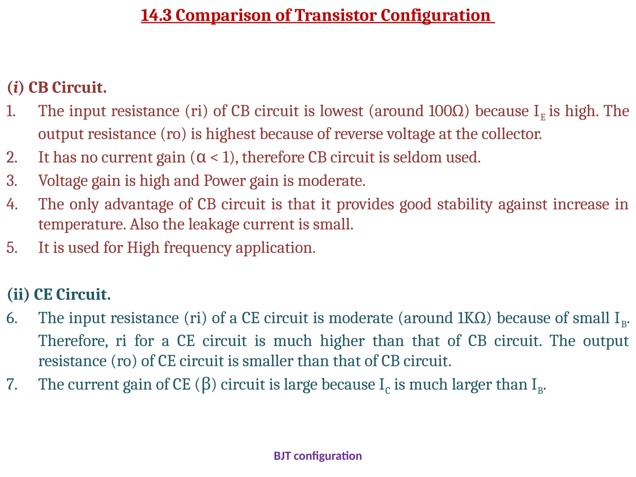
(i) CB Circuit.
1. The input resistance (ri) of CB circuit is lowest (around 100Ω) because IE is high. The
output resistance (ro) is highest because of reverse voltage at the collector.
2. It has no current gain ( < 1), therefore CB circuit is seldom used.
α
3. Voltage gain is high and Power gain is moderate.
4. The only advantage of CB circuit is that it provides good stability against increase in
temperature. Also the leakage current is small.
5. It is used for High frequency application.
(ii) CE Circuit.
6. The input resistance (ri) of a CE circuit is moderate (around 1KΩ) because of small IB.
Therefore, ri for a CE circuit is much higher than that of CB circuit. The output
resistance (ro) of CE circuit is smaller than that of CB circuit.
7. The current gain of CE ( ) circuit is large because I
β C is much larger than IB.
BJT configuration
10.
14.3 Comparison ofTransistor Configuration
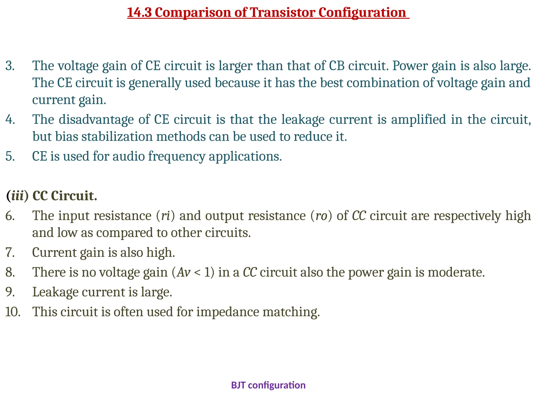
3. The voltage gain of CE circuit is larger than that of CB circuit. Power gain is also large.
The CE circuit is generally used because it has the best combination of voltage gain and
current gain.
4. The disadvantage of CE circuit is that the leakage current is amplified in the circuit,
but bias stabilization methods can be used to reduce it.
5. CE is used for audio frequency applications.
(iii) CC Circuit.
6. The input resistance (ri) and output resistance (ro) of CC circuit are respectively high
and low as compared to other circuits.
7. Current gain is also high.
8. There is no voltage gain (Av < 1) in a CC circuit also the power gain is moderate.
9. Leakage current is large.
10. This circuit is often used for impedance matching.
BJT configuration
11.
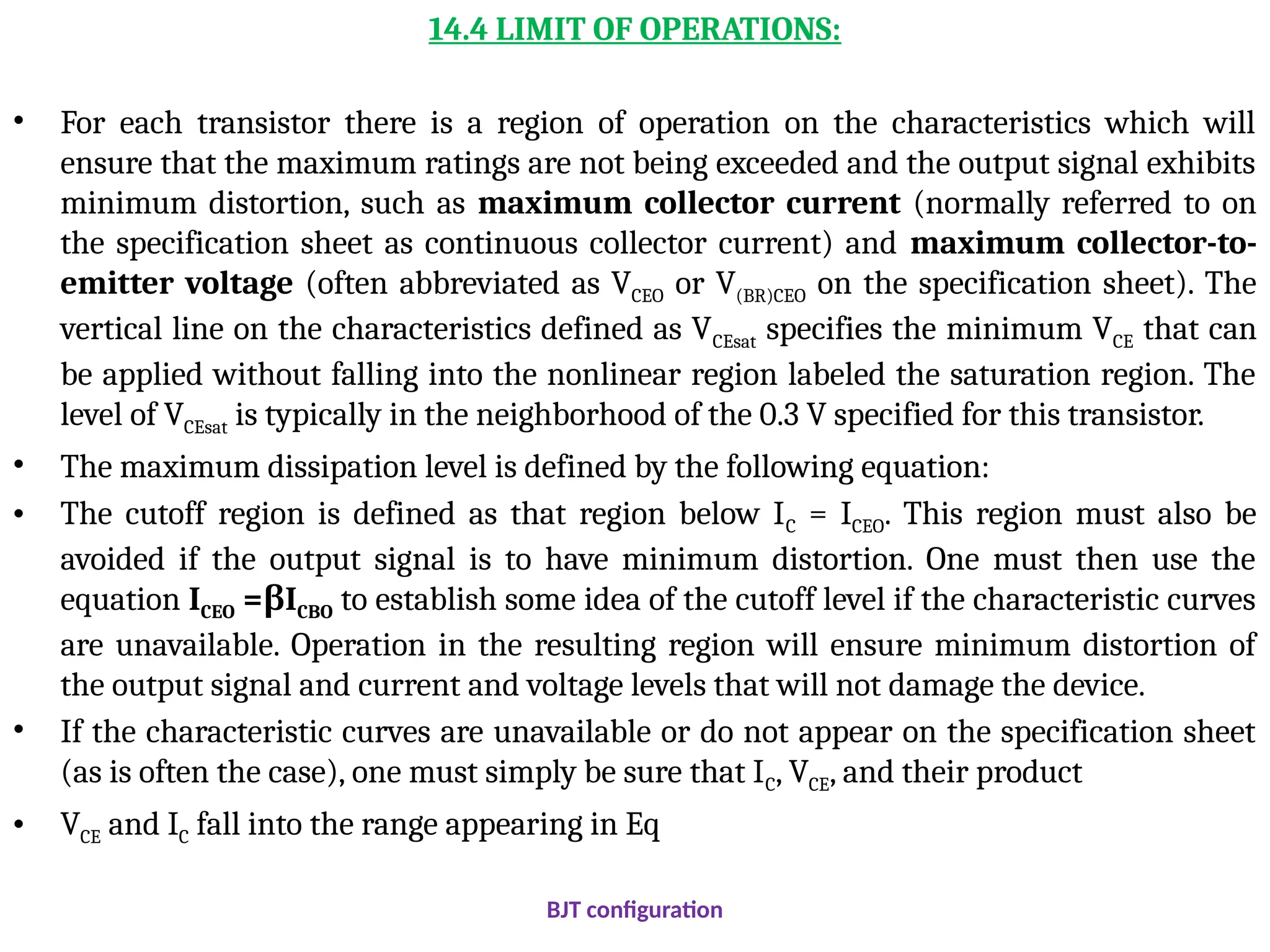
14.4 LIMIT OFOPERATIONS:
• For each transistor there is a region of operation on the characteristics which will
ensure that the maximum ratings are not being exceeded and the output signal exhibits
minimum distortion, such as maximum collector current (normally referred to on
the specification sheet as continuous collector current) and maximum collector-to-
emitter voltage (often abbreviated as VCEO or V(BR)CEO on the specification sheet). The
vertical line on the characteristics defined as VCEsat specifies the minimum VCE that can
be applied without falling into the nonlinear region labeled the saturation region. The
level of VCEsat is typically in the neighborhood of the 0.3 V specified for this transistor.
• The maximum dissipation level is defined by the following equation:
• The cutoff region is defined as that region below IC = ICEO. This region must also be
avoided if the output signal is to have minimum distortion. One must then use the
equation ICEO = I
β CBO to establish some idea of the cutoff level if the characteristic curves
are unavailable. Operation in the resulting region will ensure minimum distortion of
the output signal and current and voltage levels that will not damage the device.
• If the characteristic curves are unavailable or do not appear on the specification sheet
(as is often the case), one must simply be sure that IC, VCE, and their product
• VCE and IC fall into the range appearing in Eq
BJT configuration
![14.1 COMMON COLLECTOR [CC]CONFIGURATION:
• The Common Collector Amplifier is another type of bipolar junction transistor, (BJT)
configuration where the input signal is applied to the base terminal and the output signal
taken from the emitter terminal. Thus the collector terminal is common to both the input
and output circuits. This type of configuration is called Common Collector, (CC) because the
collector terminal is effectively “grounded” or “earthed” through the power supply.
• In many ways the common collector configuration (CC) is the reverse of the common emitter
(CE) configuration as the connected load resistor is changed from the collector terminal for
RC to the emitter terminal for RE.
• The common collector or grounded collector configuration is commonly used in impedance
matching; where high impedance input source needs to be connected to a low impedance
output load requiring a high current gain.
• The input characteristics will be a between input current IB and input voltage VBC. For all
practical purposes, the output characteristics of the common-collector configuration are the
same as for the common-emitter configuration. For the common-collector configuration the
output characteristics are a plot of IE versus VEC for a range of values of IB. The input current,
therefore, is the same for both the common-emitter and common collector characteristics.
BJT configuration](https://image.slidesharecdn.com/bee2020-21bjtconfcc-250720174352-2bcdd6f7/75/BEE-2020-21-BJT-conf-CC-pptx-transistors-3-2048.jpg)
![14.1 COMMON COLLECTOR [CC]CONFIGURATION:
• Current amplification factor γ. In common collector circuit, input current is the base
current IB and output current is the emitter current IE. The ratio of change in emitter
current ( I
Δ E) to the change in base current ( I
Δ B) is known as current amplification
factor in common collector (CC) arrangement.
BJT configuration](https://image.slidesharecdn.com/bee2020-21bjtconfcc-250720174352-2bcdd6f7/75/BEE-2020-21-BJT-conf-CC-pptx-transistors-4-2048.jpg)