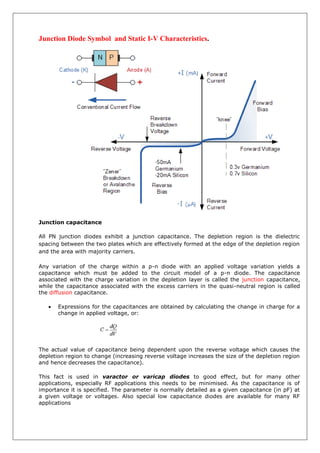
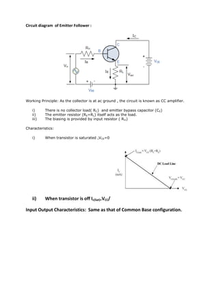
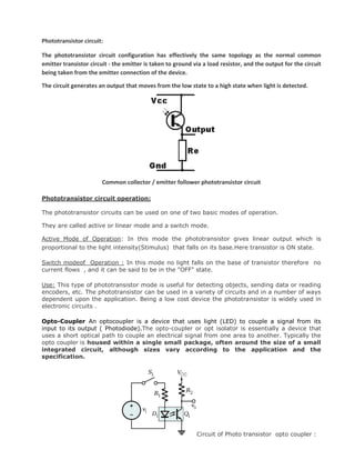
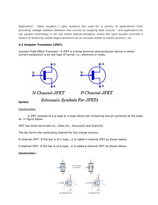
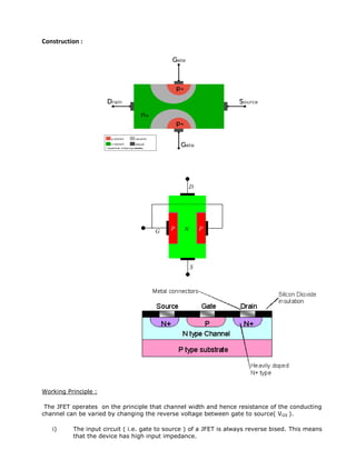
SlideShare a Scribd company logo
1 of 73
Download to read offline
Class Notes of
BET102 Basic Electronics Engineering
Common to 1st
/2nd
Semester
of
Diploma in Engineering.
Under SCTE&VT , Odisha.
Prepared By:
Rajendra Kumar Prusty
Asima Rout
Sarat Kumar Muduli
BET-102 Basic Electronics Engineering.
Chapter-1
1. ELECTRONIC DEVICES
1.1 Define Electronics & its application.
The world's reliance on electronics is so great that commentators claim people live in an
"electronic age." People are surrounded by electronics—televisions, radios, computers, mobiles,
Laptop and DVD players, along with products with major electric components, such as
microwave ovens, refrigerators, and other kitchen appliances, automatic vehicles, Robotics, as
well as hearing aids and medical instruments and numerous applications in industry.
Definition: The branch of engineering which deals with current conduction through a Vacuum
or Gas or Semiconductor is known as Electronics. An electronic device is that in which current
flows through a vacuum or gas or semiconductor. This control of electrons is accomplished by
devices that resist, carry, select, steer, switch, store, manipulate, and exploit the electron.
Or
Electronics deals with electrical circuits that involve active electrical components such as
vacuum tubes, transistors, diodes and integrated circuits, and associated passive
interconnection technologies. Commonly, electronic devices contain circuitry consisting
primarily or exclusively of active semiconductors supplemented with passive elements; such a
circuit is described as an electronic circuit.
Pre Knowledge (Some of the basic definitions):
Passive Components: Capable of operating without an external power source. Typical passive
components are resistors, capacitors, inductors.
Active components: Requiring a source of power to operate. Includes transistors (all types), integrated
circuits (all types), TRIACs, SCRs, LEDs, etc.
APPLICATIONS of Electronics:
Electronic components: capacitor (C), cathode ray tube (CTR), diode (D), digital signal
processor (DSP, field effect transistor (FET), integrated circuit (IC), junction gate field effect
transistor (JFET), inductor (L), Liquid crystal display (LCD), light dependent resistor (LDR, light
emitting diode (LED), Metal oxide semiconductor field effect transistor (MOSFET), transistor
(Q), resistor (R), relay (RLA, RY), switch (SW), transformer (T), thermistor (TH), transistor
(Tr), integrated circuit (U, IC), variable capacitor (VC), variable resistor (VR) and more.
Consumer Electronics include products like – Audio Systems, Video Systems, TV (Television),
Computer, Laptop, Digital Camera, DVD Players, Home and Kitchen Appliances, GPS, Mobiles
Phones etc.
Communication. Electronic communication systems connect people around the world. Using
telephones, Internet and computers, people in different countries communicate almost
instantly. Radios transmit sounds and televisions transmit sounds and pictures great distances.
Cellular telephones enable a person to call another person. Within seconds, fax machines send
and receive copies of documents over telephone lines/Satellite.
Information processing. Scientists, artists, students, government and business workers, and
hobbyists at home all rely on computers, Internet to handle huge amounts of information
quickly and accurately. Computers solve difficult mathematical problems, maintain vast
amounts of data, create complex simulations, and perform a multitude of other tasks that help
people in their everyday lives.
Medicine and research. Include product like X-ray machines ECG (Electrocardiogram) use
radiation to take images of bones and internal organs. Radiation therapy, or radiotherapy, uses
X-rays and other forms of radiation to fight cancer. Many hearing-impaired people depend on
hearing aids to electrically amplify sound waves.
Computers and other electronic instruments provide scientists and other researchers with
powerful tools to better understand their area of study. Computers, for example, help scientists
design new drug molecules, track weather systems, and test theories about how galaxies and
stars develop. Electron microscopes use electrons rather than visible light to magnify specimens
1 million times or more.
Automation. Electronic components enable many common home appliances, such as
refrigerators, washing machines, and toasters, to function smoothly and efficiently. People can
electronically program coffeemakers, lawn sprinklers, and many other products to turn on and
off automatically. Microwave ovens heat food quickly by penetrating it with short radio waves
produced by a vacuum tube.
Instrumentation. Measuring Instruments like CRO, Multimeter, ph-meter, strain gauge,
VTVM, Frequency Counter are used in different Laboratory/organisations.
Many automobiles have electronic controls in their engines and fuel systems. Electronic devices
also control air bags, which inflate to protect a driver and passengers in a collision.
1.2 Define Electronic Emission & different types of Emission.
The Electronics devices depends the movements of free Electrons in an evacuated space.
The liberation of electrons from the surface of a metal is known as Electron Emission.
 For electron emission, metals are used because they have many free electrons.
 The electrons are free only to transfer from one atom to another within the metal but
they cannot leave the metal surface to provide electron emission.
 Thus at the surface of the metal, a free electron encounters forces that prevent it to
leave the metal.
 In other words, the metallic surface offer a barrier to free electrons, their kinetic
energy increases and is known as surface barrier.
 However, if sufficient energy is given to the free electrons, their kinetic energy
increases and thus the electrons will cross over the surface barrier to leave the metal.
 This additional energy required by an electron to overcome the surface barrier of the
metal is called work function of the metal.
The metallic surface offers a barrier to free electrons and is known as surface barrier.
Work function (W0): The amount of additional energy(such as heat energy, energy stored in
electric field, light energy or kinetic energy of the electric charges bombarding the metal
surface) required to emit an electron from a metallic surface is known as work function of that
metal. The minimum energy required by an electron to just escape (i.e. with zero velocity) from
metal's surface is called Work function (W0) of the metal. The work function of pure metals
varies (roughly) from 2eV to 6eV. Its value depends upon the nature of the metal, its purity
and the conditions of the surface.
Different types of Emission:
There are following four principal method of obtaining electron emission from the surface of a
metal:
1. Thermionic Emission - (Due to Thermal energy)
2. Field Emission - (Due to application of strong electric field)
3. Secondary Emission – ( due to bombardment of high-speed electrons)
4. Photo Electric Emission – ( by the application of light)
1. Thermionic Emission
The process of electron emission from a metal surface by supplying thermal energy to it is
known as Thermionic emission.
In this type of emission the electron emission is achieved by heating the electrode to a
sufficient temperature (about 2500o
C) to enable the free electrons to leave the metal surface.
Due to heating the electrons get enough energy that they emit from the surface of that material
heat energy is converted into kinetic energy, causing accelerated motion of free electrons and
electrons acquire additional energy equal to the work function of the metal. An electron emitted
from a hot cathode comes out with a velocity that presents different between the kinetic energy
possessed by electron just before emission usually used in cathode of diode, triode, pentode,
CRT and many other. The higher the temperature, the greater is the emission of electrons. The
commonly used materials for electron emission are tungsten, thoriated tungsten and metallic
oxides of barium and strontium.
S.No. Emitter Work Function Operating Temperature
1 Tungsten 4.52 eV 2327ºC
2 Thoriated tungsten 2.63 eV 1700ºC
3 Oxide-coated 1.1 eV 750ºC
2. Field Emission
The process of electron emission by the application of strong electric field at the surface of a
metal is known as field emission.
When metal surface is placed in an electric field, the electron rotating in their orbits
experience a force due to electrostatic field. Hence the process of electron emission by
application of strong electric field at the surface of a metal is called field emission. It is also
called cold cathode emission or auto- electronic emission.
3. Secondary Emission
Electron emission from a metallic surface by the bombardment of high-speed electrons
or other particles is known as secondary emission.
When high-speed electrons suddenly strike a metallic surface, they may give some or all
of their kinetic energy to the free electrons in the metal. If the energy of the striking
electrons is sufficient, it may cause free electrons to escape from the metal surface. This
phenomenon is called secondary emission. The electrons that strike the metal are called
primary electrons while the emitted electrons are known as secondary electrons. The
intensity of secondary emission depends upon the emitter material, mass and energy of the
bombarding particles.
4. Photo Electric Emission
Electron emission from a metallic surface by the application of light is known as photo
electric emission.
When a beam of light strikes the surface of cathode normally made of potassium, Sodium the
energy of photons of light is transfer to the free electrons of cathode. In this method, the
energy of light falling upon the metal surface is transferred to the free electrons within the
metal to enable them to leave the surface. The greater the intensity of light beam falling on the
metal surface, the greater is the photoelectric emission. The emitted electrons are known as
photo electrons and the phenomenon is known as photoelectric emission. Photo-electric
emission is utilised in photo tubes which form the basis of television and sound films.
1.3 Classification of solid according to electrical conductivity (Conductor, Semiconductor &
Insulator) with respect to energy band diagram only.
Pre-Knowledge:
(i) Valence band. The range of energies (i.e. band) possessed by valence electrons is
known as valence band. The electrons in the outermost orbit of an atom are known as
valence electrons. This band may be completely or partially filled.
(ii) Conduction band.
The range of energies (i.e. band) possessed by conduction band electrons is known as
conduction band. Generally, insulators have empty conduction band. On the other
hand, it is partially filled for conductors. The free electrons which are responsible for the
conduction of current in a conductor are called conduction electrons.
(iii) Forbidden energy gap. The separation between conduction band and valence
band on the energy level diagram is known as forbidden energy gap.
Fig 1. Energy band diagram
Classification:
Solid-state materials According to electrical conductivity can be classified into three
groups. Such as:
1. Insulators - Insulators are materials having an electrical conductivity
(like diamond: 10-14S/cm);
2. Semiconductors - semiconductors have a conductivity (for
silicon it can range from 10-5S/cm to 103S/cm)
3. Conductors - at last conductors are materials with high conductivities:
(like silver: 106S/cm.)
Figure 2 : Representation of energy bands
(i) Insulators. Insulators (e.g. wood, glass, plastics,rubber etc.) are those substances which do
not allow the passage of electric current through them. In terms of energy band, the
valence band is full while the conduction band is empty as shown in Fig 2. Further, the
energy gap between valence and conduction bands is very large (15 eV). Therefore, a very
high electric field is required to push the valence electrons to the conduction band. For this
reason, the electrical conductivity of such materials is extremely small. At room
temperature, the valence electrons of the insulators do not have enough energy to cross
over to the conduction band. However, when the temperature is raised, some of the
valence electrons may acquire enough energy to cross over to the conduction band. Hence,
the resistance of an insulator decreases with the increase in temperature i.e. an insulator
has negative temperature coefficient of resistance.
(ii) Conductors. Conductors (e.g. copper, aluminum) are those substances which easily allow
the passage of electric current through them. It is because there are a large number of free
electrons available in a conductor. In terms of energy band as in Fig 2, the valence and
conduction bands overlap each other due to this overlapping; a slight potential difference
across a conductor causes the free electrons to constitute electric current.
(iii) Semicondutors. Semiconductors (e.g. germanium, silicon etc.) are those substances
whose electrical conductivity lies in between conductors and insulators. In terms of energy
band, the valence band is almost filled and conduction band is almost empty in fig 2.
Further, the energy gap between valence and conduction bands is very small. The
semiconductor has :
(a) Filled valence band
(b) Empty conduction band
(c) Small energy gap or forbidden gap ( 1 eV) between valence and conduction bands.
(d) Semiconductor virtually behaves as an insulator at low temperatures. However, even at
room temperature, some electrons cross over to the conduction band, imparting little
conductivity (i.e. conductor).
1.3 Discuss Intrinsic & Extrinsic Semiconductor.
Intrinsic Semiconductor
A semiconductor in an extremely pure form is known as an intrinsic semiconductor.
In this case the holes in the valence band are vacancies created by electrons that have been
thermally excited to the conduction band and hole-electron pairs are created. When electric
field is applied across an intrinsic semiconductor, the current conduction takes place by two
processes, namely; by free electrons and holes as shown in Fig 3. The free electrons are
produced due to the breaking up of some covalent bonds by thermal energy. At the same time,
holes are created in the covalent bonds. Under the influence of electric field, conduction
through the semiconductor is by both free electrons and holes. Therefore, the total current
inside the semiconductor is the sum of currents due to free electrons and holes. This creates
new holes near the positive terminal which again drift towards the negative terminal.
Figure 3 : Diagram showing the electronic bonds in an intrinsic semiconductor (Si)
Extrinsic Semiconductor
An extrinsic semiconductor is a semiconductor doped by addition of small amount
impurity which is able to change its electrical properties (conduction), making it suitable for
electronic applications (diodes, transistors, etc.) or optoelectronic applications (light emitters
and detectors). This is achieved by adding a small amount of suitable impurity (having 3 or 5
valence electron) to a semiconductor (having 4 valence electron). It is then called impurity or
extrinsic semiconductor.
 The process of adding impurities to a semiconductor is known as doping. The purpose of
adding impurity is to increase either the number of free electrons or holes in the
semiconductor crystal.
 If a penta valent impurity (having 5 valence electrons) is added to the semiconductor, a
large number of free electrons are produced in the semiconductor.
 If a trivalent impurity (having 3 valence electrons) is added to the semiconductor, large
number of holes are produced in the semiconductor crystal.
 Depending upon the type of impurity added, extrinsic semiconductors are classified into:
(i) n-type semiconductor
(ii) p-type semiconductor
(i) n-type Semiconductor
When a small amount of pentavalent impurity is added to a pure semiconductor, it is known as n-type
semiconductor.
The addition of pentavalent impurity pro-vides a large number of free electrons in the
semiconductor crystal. Typical examples of pentavalent impurities are arsenic ,
antimony,Bismuth and Phosphorous etc. Such impurities which produce n-type semiconductor
are known as donor impurities because they donate or provide free electrons to the
semiconductor crystal.
Figure 4 : Schematic representation of electronic bonds in a Silicon crystal doped with Arsenic As (n
doping)
 Electrons are said to be the majority carriers whereas holes are the minority carriers.
(ii) p-type Semiconductor
When a small amount of trivalent impurity is added to a pure semiconductor, it is called p-type
Semiconductor.
The addition of trivalent impurity provides a large number of holes in the semiconductor.
Typical examples of trivalent impurities are gallium , indium, boron etc. Such impurities which
produce p-type semiconductor are known as acceptor impurities because the holes created can
accept the electrons fig 5.
Figure 5 : schematic representation of a Si crystal doped with boron (B)
Electrons are said to be the minority carriers whereas holes are the majority carriers.
1.4 Explain the difference between vacuum tube & semiconductor.
Figure 6: Vacuum tubes
Vacuum Tubes:
Advantages
1. Superior sound quality.
2. Can handle large currents
3. Tolerant of large overloads and voltage spikes.
4. Characteristics highly independent of temperature, greatly simplifying biasing.
5. Wider dynamic range than transistors circuits, due to higher operating voltages and
overload tolerance.
6. Capacitive coupling can be done with small, high-quality film capacitors, due to
inherently high-impedances of tube circuits.
7. Operation is usually in Class A or Class AB, minimizing crossover notch distortion.
8. Tubes can be relatively easily replaced by user.
Disadvantages
1. Bulky(Larger in Size), hence not suitable for portable products
2. Higher operating voltages required.
3. High power consumption; needs heater supply that generates waste heat and yields
lower efficiency, notably for small-signal circuits.
4. Glass tubes are fragile, compared to metal transistors.
5. Cathode electron-emitting materials are used up in operation.
6. High-impedance devices that need impedance matching transformer for low-impedance
loads, like speakers; however, the magnetic cushion provided by an output transformer
prevents the output tubes from blowing up.
7. Sometimes higher cost than equivalently powered transistors.
8. Complicated in manufacturing process.
Transistors:
Advantages
1. Usually smaller size, lower cost and longer life.
2. Can handle small current
3. Can be combined in the millions on one cheap die to make an integrated circuit, whereas
tubes are limited to at most three functional units per glass bulb.
4. Lower power consumption, less waste heat, and high efficiency than equivalent tubes,
especially in small-signal circuits.
5. Can operate on lower-voltage supplies for greater safety, lower costs, tighter clearances.
6. Usually more physical ruggedness than tubes (depends upon construction).
Disadvantages
1. Tendency toward higher distortion
2. Complex circuits and considerable negative feedback required for low distortion.
3. Large unit-to-unit manufacturing tolerances and unreliable variations in key parameters,
such as gain and threshold voltage.
4. Device parameters vary considerably with temperature, complicating biasing and
increasing likelihood of thermal runaway.
5. Cooling is less efficient than with tubes, because lower operating temperature is required
for reliability. Tubes prefer hot; transistors do not. Massive, expensive and unwieldy
heat sinks are always required for power transistors, yet they are not always effective
(power output transistors still blow up; whereas, tubes fade down gracefully over time
with warning.)
6. Less tolerant of overloads and voltage spikes than tubes.
7. Capacitive coupling usually requires high-value electrolytic capacitors, which give audibly
and measurably inferior performance at audio frequency extremes.
8. Greater tendency to pick up radio frequency interference and self-oscillate to the point
of self-destruction, due to rectification by low-voltage diode junctions or slew-rate
effects.
9. Maintenance more difficult; devices are not easily replaced by user.
1.5 State basic concept of Integrated Circuits (I.C) & its use.
Figure 7: Integrated Circuits
An integrated circuit (IC), sometimes called a chip or microchip, is a semiconductor wafer on
which thousands or millions of tiny resistors, capacitors, and transistors are fabricated. An IC
can function as an amplifier, oscillator, timer, counter, computer memory, or microprocessor. A
particular IC is categorized as either linear analog or digital, depending on its intended
application. IC's are are of Linear , digital and mixed types
Linear ICs have continuously variable output (theoretically capable of attaining an infinite
number of states) that depends on the input signal level. As the term implies, the output signal
level is a linear function of the input signal level. Linear ICs are used as audio-frequency (AF)
and radio-frequency (RF) amplifiers. The operational amplifier (op amp) is a common device in
these applications.
Digital ICs operate at only a few defined levels or states, rather than over a continuous range of
signal amplitudes. These devices are used in computers, computer networks, modems, and
frequency counters. The fundamental building blocks of digital ICs are logic gates, which work
with binary data, that is, signals that have only two different states, called low (logic 0) and
high (logic 1).
Applications and Uses of Integrated Circuits
The advantages of Integrated Circuits are:
1. Very small size: Hundred times smaller than the discrete circuits.
2. Lesser weight: As large number of components can be packed into a single chip, weight is reduced
3. Reduced cost: The mass production technique has helped to reduce the price,
4. High reliability: Due to absence of soldered connection, few interconnections and small temperature
rise failure rate is low.
5. Low power requirement: As the size is small power consumption is less.
6. Easy replacement: In case of failure chip can easily be replaced.
Linear IC's also known as analog Integrated circuits are:
1. Power amplifiers
2. Small-signal amplifiers
3. Operational amplifiers
4. Microwave amplifiers
5. RF and IF amplifiers
6. Voltage comparators
7. Multipliers
8. Radio receivers
9. Voltage regulators
Digital IC's are mostly used in computers. They are also referred as switching circuits because their input and
output voltages are limited to two levels - high and low i.e. binary. They include:
1. Flip-flops
2. Logic gates
3. Timers
4. Counters
5. Multiplexers
6. Calculator chips
7. Memory chips
8. Clock chips
9. Microprocessors
10. Microcontrollers
11. Temperature sensors
Mixed type applications - cars (automotive controls), televisions, computers, microwaves,
portable devices like laptops, MP3, play stations, cameras, cellular phones to ship equipments,
aero planes, space craft’s. These are also used in switching telephone circuits and data
processing. They also found applications in military equipments. The most common application
of IC is digital watch which tells hour, second, minute, day and month. Another common but
important application is scientific calculator which can perform basic functions like addition,
subtraction, multiplication and division as well as complex functions like square root, cube,
permutations, combinations , trigonometric functions, etc
Chapter Review Questions:
1. Define Electronics & its application.
2. Define work function.
3. Define Electronic Emission & different types of Emission.
4. Explain Conductor, Semiconductor & Insulator with respect to energy band
diagram only.
5. Define doping.
6. Define energy gap & valence electrons
7. Discuss Intrinsic Semiconductor.
8. Discuss Extrinsic Semiconductor.
9. Explain the difference between vacuum tube & semiconductor.
10. State basic concept of integrated circuits (I.C) & its use.
11. Define accepter & donor atom
12. List different types of Impurity.
Chapter-2
2.1 Define Rectifier & state its use.
The conversion of bidirectional alternating current (a.c.) into unidirectional direct current (d.c.)
is called rectification. Electronic devices can convert a.c. power into d.c. power with very high
efficiency.
Example-Diodes : Diodes are useful electrical components for rectification purposes. Diodes are
used in many applications like the following.
 Converting AC power from the 60Hz line into DC power for radios, televisions, telephone
answering machines, computers, and many other electronic devices.
 Converting radio frequency signals into audible signals in radios.
 used as rectifier in DC Power Supplies.
 In Demodulation or Detector Circuits.
 In clamping networks used as DC Restorers
 In clipping circuits used for waveform generation.
 As switches in digital logic circuit
2.1.1 Rectifying diode
Review of P-type and N-type semiconductor junction of P-type & N-type i.e. PN junction Barrier
voltage, depletion region, Junction Capacitance.
A p–n junction is a boundary or interface between two types of semiconductor material,
p-type and n-type, inside a single crystal of semiconductor. p–n junctions are
elementary "building blocks" of most semiconductor electronic devices such as
diodes, transistors, solar cells, LEDs, and integrated circuits. After joining p-type
and n-type semiconductors, electrons from the n region near the p–n interface tend to
diffuse into the p region. The regions nearby the p–n interfaces lose their neutrality and
become charged, forming the space charge region or depletion layer
Fig 8 (a) Blocks of P and N semiconductor in contact have no exploitable properties. (b) Single
crystal doped with P and N type impurities develops a potential barrier.
This separation of charges at the PN junction constitutes a potential barrier. This potential
barrier must be overcome by an external voltage source to make the junction conduct.
PN Junction Diodes
Example: Circuit symbol:
Function
Diodes allow electricity to flow in only one direction. The arrow of the circuit symbol shows the
direction in which the current can flow.
Forward Voltage Drop
When a forward voltage is applied to diode, a small voltage
experiences across a conducting diode, it is called the
forward voltage drop and is about 0.7V for all normal
diodes which are made from silicon. The forward voltage drop
of a diode is almost constant whatever the current passing
through the diode so they have a very steep characteristic
(current-voltage graph).
Reverse Voltage
When a reverse voltage is applied a perfect diode does not conduct, but all real diodes leak a very
tiny current of a few µA or less. This can be ignored in most circuits because it will be very much
smaller than the current flowing in the forward direction. However, all diodes have a maximum
reverse voltage (usually 50V or more) and if this is exceeded the diode will fail and pass a large
current in the reverse direction, this is called breakdown.
Ordinary diodes can be split into two types: Signal diodes which pass small currents of 100mA
or less and Rectifier diodes which can pass large currents. In addition there are other types of
diodes as such : LEDs, Zener diodes ,Tunnel diode,PIN diode,Photo diode and Varicap diode etc.
Practical Knowledge:
Connecting and soldering
Diodes must be connected the correct way round, the diagram may
be labeled a or + for anode and k or - for cathode (yes, it really is
k, not c, for cathode!). The cathode is marked by a line painted on
the body. Diodes are labeled with their code in small print, you
may need a magnifying glass to read this on small signal diodes!
Small signal diodes can be damaged by heat when soldering, but
the risk is small unless you are using a germanium diode (codes beginning OA...) in which
case you should use a heat sink clipped to the lead between the joint and the diode body. A
standard crocodile clip can be used as a heat sink.
Signal diodes (small current)
Signal diodes are used to process information (electrical signals) in circuits, so they are only
required to pass small currents of up to 100mA.
General purpose signal diodes such as the 1N4148 are made from silicon and have a forward
voltage drop of 0.7V.
Germanium diodes such as the OA90 have a lower forward voltage drop of 0.2V and this
makes them suitable to use in radio circuits as detectors which extract the audio signal from
the weak radio signal.
For general use, where the size of the forward voltage drop is less important, silicon diodes are
better because they are less easily damaged by heat when soldering, they have a lower
resistance when conducting, and they have very low leakage currents when a reverse voltage is
applied.
Biasing of Diode: The process of applying an external voltage is called as “biasing”.
Pre Knowledge:
Zero Bias: When no external voltage potential is applied to the PN junction diode called Zero
Biased Junction Diode. However if the diodes terminals are shorted together, a few holes
(majority carriers) in the P-type material with enough energy to overcome the potential barrier
will move across the junction against this barrier potential. This is known as the “Forward
Current” and is referenced as IF.. Likewise, holes generated in the N-type material (minority
carriers) and move across the junction in the opposite direction. This is known as the “Reverse
Current” and is referenced as IR. This transfer of electrons and holes back and forth across the
PN junction is known as diffusion, as shown Fig 9.
Fig 9: Zero Bias
But how ever there are two ways in which we can bias a pn junction diode.
1) Forward bias
2) Reverse bias
Forward Bias – The voltage potential is connected positive, (+ve) to the P-type material and negative, (-ve)
to the N-type material across the diode which has the effect of Decreasing the PN junction diodes’s width.
Reverse Bias – The voltage potential is connected negative, (-ve) to the P-type material and positive, (+ve) to
the N-type material across the diode which has the effect of Increasing the PN junction diode’s width.
2.1.2 Forward & Reverse bias & V-I characteristics of PN junction Diode
Forward Biased PN Junction Diode
When a diode is connected in a Forward Bias condition, a negative voltage is applied to the n-
type material and a positive voltage is applied to the p-type material. If this external voltage
becomes greater than the value of the potential barrier, approx. 0.7 volts for silicon and 0.3
volts for germanium, the potential barriers opposition will be overcome and current will start to
flow.
Forward Characteristics Curve for a Junction Diode
The application of a forward biasing voltage on the junction diode results
 the depletion layer becoming very thin and narrow which represents a low impedance
path through the junction thereby allowing high currents to flow.
 The point at which this sudden increase in current takes place is represented on the
static I-V characteristics curve above as the “knee” point.
Reduction in the Depletion Layer due to Forward Bias
Reverse Biased PN Junction Diode
When a diode is connected in a Reverse Bias condition, a positive voltage is applied to the N-
type material and a negative voltage is applied to the P-type material. The positive voltage
applied to the N-type material attracts electrons towards the positive electrode and away from
the junction, while the holes in the P-type end are also attracted away from the junction
towards the negative electrode. Thus
 the depletion layer grows wider due to a lack of electrons and holes and presents a high
impedance path, almost an insulator.
 The result is that a high potential barrier is created thus preventing current from flowing
through the semiconductor material.
 a high resistance value to the PN junction and practically zero current flows through the
junction diode with an increase in bias voltage. However, a very small leakage current
does flow through the junction which can be measured in microamperes, ( μA ).
Increase in the Depletion Layer due to Reverse Bias
Reverse Characteristics Curve for a Junction Diode
Junction Diode Symbol and Static I-V Characteristics.
Junction capacitance
All PN junction diodes exhibit a junction capacitance. The depletion region is the dielectric
spacing between the two plates which are effectively formed at the edge of the depletion region
and the area with majority carriers.
Any variation of the charge within a p-n diode with an applied voltage variation yields a
capacitance which must be added to the circuit model of a p-n diode. The capacitance
associated with the charge variation in the depletion layer is called the junction capacitance,
while the capacitance associated with the excess carriers in the quasi-neutral region is called
the diffusion capacitance.
 Expressions for the capacitances are obtained by calculating the change in charge for a
change in applied voltage, or:
The actual value of capacitance being dependent upon the reverse voltage which causes the
depletion region to change (increasing reverse voltage increases the size of the depletion region
and hence decreases the capacitance).
This fact is used in varactor or varicap diodes to good effect, but for many other
applications, especially RF applications this needs to be minimised. As the capacitance is of
importance it is specified. The parameter is normally detailed as a given capacitance (in pF) at
a given voltage or voltages. Also special low capacitance diodes are available for many RF
applications
Junction Diode Summary
The PN junction region of a Junction Diode has the following important characteristics:
 Semiconductors contain two types of mobile charge carriers, Holes and Electrons.
 The holes are positively charged while the electrons negatively charged.
 A semiconductor may be doped with donor impurities such as Antimony (N-type doping),
so that it contains mobile charges which are primarily electrons.
 A semiconductor may be doped with acceptor impurities such as Boron (P-type doping),
so that it contains mobile charges which are mainly holes.
 The junction region itself has no charge carriers and is known as the depletion region.
 The junction (depletion) region has a physical thickness that varies with the applied
voltage.
 When a diode is Zero Biased no external energy source is applied and a natural
Potential Barrier is developed across a depletion layer which is approximately 0.5 to
0.7v for silicon diodes and approximately 0.3 of a volt for germanium diodes.
 When a junction diode is Forward Biased the thickness of the depletion region reduces
and the diode acts like a short circuit allowing full current to flow.
 When a junction diode is Reverse Biased the thickness of the depletion region
increases and the
2.1.2 Specifications:-(Definition)
Forward voltage drop, Reversed saturation current, maximum forward current ,power dissipation
Package view of diodes of different power ratings(to be shown during practical hours)
The list below provides details of the various diode characteristics, and diode parameters found in
the datasheets and specifications for diodes.
 Semiconductor material: Silicon is the most widely used material as if offers high
levels of performance for most applications and it offers low manufacturing costs. The
other material that is used is germanium. Germanium materials are generally reserved
for more specialist diodes.
 Forward voltage drop (Vf): The voltage across a PN junction diode arise for two
reasons. The first of the nature of the semiconductor PN junction and results from the
turn-on voltage mentioned above. This voltage enables the depletion layer to be
overcome and for current to flow. The second arises from the normal resistive losses in
the device. It is the instantaneous forward voltage that a pn junction can conduct
without damage the pn junction.
 Peak Inverse Voltage (PIV): It is the maximum voltage a diode can withstand in the
reverse direction without damage to pn junction.
 Maximum forward current: It is the maximum instantaneous forward current that a
pn junction can conduct without damage the pn junction When designing a circuit that
passes any levels of current it is necessary to ensure that the maximum current levels
for the diode are not exceeded. As the current levels rise, so additional heat is dissipated
and this needs to be removed.
 Maximum power ratting: It is the maximum power that can be dissipated without
damage the pn junction.
2.2 Zener Diode :Construction (reference to doping level)
2.2.2 Symbol ,circuit diagram for characteristics (forwarded & reversed
Zener diodes
Circuit symbol:
Zener diodes or as they may sometimes be called, reference diodes operate like an ordinary
diode in the forward bias direction. They have the normal turn on voltage of 0.6 volts for a
silicon diode. However in the reverse direction their operation is rather different. Zener diodes
are used to maintain a fixed voltage. They are designed to 'breakdown' in a reliable and non-
destructive way so that they can be used in reverse to maintain a fixed voltage across their
terminals. The diagram shows how they are connected, with a resistor in series to limit the
current.
Zener diodes can be distinguished from ordinary diodes by their code and breakdown voltage
which are printed on them. Zener diode codes begin BZX... or BZY... Their breakdown voltage
is printed with V in place of a decimal point, so 4V7 means 4.7V for example. Some of Zener
diodes are rated by their breakdown voltage and maximum power:
 The minimum voltage available is 2.7V.
 Power ratings of 400mW and 1.3W are common.
Zener v-i characteristic
The vi characteristic of the Zener to voltage reference diode is the key to its operation. In the
forward direction, the diode performs like any other, but it is in the reverse direction where its
specific performance parameters can be utilised.
Fig 10 Zener diode characteristic
Although the voltage reference diode is normally referred to as a Zener diode, there are two
different breakdown mechanisms that can occur:
 Zener effect: This effect predominates below 5.5 volts.
 Impact ionisation: This effect predominates above 5.5 volts.
Simple Zener diode circuit for voltage regulator
When used in a regulator circuit, the Zener diode must
have the current entering it limited. If a perfect
voltage source was placed across it, then it would
draw excessive current once the breakdown voltage
had been reached. To overcome this the Zener diode
must be driven by a current source. This will limit the
current to the chosen value. The value of the series
resistor is simple to calculate. It is simply the voltage
across the resistor, divided by the current required.
The level of Zener current can be chosen to suit the
circuit and the Zener diode used.
Fig 12 Simple circuit of a Zener diode shunt regulator
Application of Zener
Used in Voltage Stabilizer, Clipper Circuit, Reference voltage limiter circuits
2.2.3 Differences between avalanche & zerner breakdown?
Zener breakdown:
In Zener breakdown the electrostatic attraction between the negative electrons and a large positive voltage
is so great that it pulls electrons out of their covalent bonds and away from their parent atoms. ie Electrons
are transferred from the valence to the conduction band. In this situation the current can still be limited by
the limited number of free electrons produced by the applied voltage so it is possible to cause Zener
breakdown without damaging the semiconductor. The important points are:
 Both sides of PN junction are heavily doped
 Depletion layer is narrow
 A strong electric field is produced
 Large number of holes and electrons are produced
 Zener current is independent of applied voltage
Avalanche breakdown
Avalanche breakdown occurs when the applied voltage is so large that electrons that are pulled
from their covalent bonds are accelerated to great velocities. These electrons collide with the
silicon atoms and knock off more electrons. These electrons are then also accelerated and
subsequently collide with other atoms. Each collision produces more electrons which leads to
more collisions etc. The current in the semiconductor rapidly increases and the material can
quickly be destroyed. The important points are:
 Both sides of PN junction are lightly doped
 Depletion layer is large
 Electric field is not so strong
 Electron hole pairs are generated
 Charge carriers acquire energy from the applied potential
2.3. (i)Special Diodes :
Tunnel Diode
The tunnel diode is a form of very fast semiconductor diode that can operate well into the
microwave radio frequency region.
Tunnel diode circuit symbol
Despite the operation of the tunnel diode. its circuit symbol as shown in fig. 13 is based on that
for the standard diode, but has 'tails' added to the bar element of the symbol to differentiate it
from other forms of PN junction diode.
Fig 13-Tunnel diode circuit symbol
Tunnel diode theory basics
Tunneling is an effect that is caused by quantum mechanical effects when electrons pass
through a potential barrier. It can be visualized in very basic terms by them "tunneling" through
the energy barrier. The tunneling only occurs under certain conditions. It occurs within tunnel
diodes because of the very high doping levels employed.
At reverse bias, the electrons tunnel from the valence band in the p-type material to the
conduction band in the n-type material, and the level of the current increase monotonically The
characteristic curve for a tunnel diode shows an area of negative resistance. When forward
biased the current in the diode rises at first, but later it can be seen to fall with increasing
voltage, before finally rising again.
It is also interesting to note that current also flows in the reverse direction - the reverse
breakdown voltage is actually zero and the diode conducts in the reverse direction. The
characteristics near the original are virtually symmetrical.
Fig 14 Tunnel diode VI characteristic
The reason for this is that there are a number of different components to forming the overall
curve.
 Normal diode current: This is the 'normal' current that would flow through a PN
junction diode.
 Tunneling current: This is the current that arises as a result of the tunneling effect.
 Excess current: This is a third element of current that contributes to the overall
current within the diode. It results from what may be termed excess current that results
from tunneling though bulk states in the energy gap, and means that the valley current
does not fall to zero.
Advantages
 Very high speed: The high speed of operation means that the tunnel diode can be
used for microwave RF applications.
 Longevity: Studies have been undertaken of the tunnel diode and its performance has
been shown to remain stable over long periods of time, where other semiconductor
devices may have degraded.
Disadvantages
 Reproducibility: It has not been possible to make the tunnel diode with as
reproducible performance to the levels often needed.
 Low peak to valley current ratio: The negative resistance region and the peak to
valley current is not as high as is often be required to produce the levels of performance
that can be attained with other devices.
Applications
Oscillator circuits: Tunnel diodes can be used as high frequency oscillators as the transition
between the high electrical conductivity is very rapid. They can be used to create oscillation as
high as 5Gz. Even they are capable of creativity oscillation up to 100 GHz in a appropriate
digital circuits.
Used in microwave circuits: Normal diode transistors do not perform well in microwave
operation. So, for microwave generators and amplifiers tunnel diode are. In microwave waves
and satellite communication equipments they were used widely, but now a day’s their uses is
decreasing rapidly as transistor for working in wave frequency area available in market.
Resistant to nuclear radiation: Tunnel diodes are resistant to the effects of magnetic fields, high
temperature and radioactivity. That’s why these can be used in modern military equipment.
These are used in nuclear magnetic resource machine also. But the most important field of its
use satellite communication equipments.
(ii) Optical Diodes :- LED, IRLED & photodiode (Symbol, working principal & applications of each)
Light emitting diode (LED)
A light emitting diode (LED) is known to be one of the best optoelectronic devices. The device is
capable of emitting a fairly narrow bandwidth of visible or invisible light when its internal diode
junction attains a forward electric current or voltage. The visible lights that an LED emits are
usually orange, red, yellow, or green. The invisible light includes the infrared light.
We know that a P-N junction can connect the absorbed light energy into its proportional electric
current. The same process is reversed here. That is, the P-N junction emits light when energy is
applied on it. This phenomenon is generally called electro luminance, which can be defined as
the emission of light from a semi-conductor under the influence of an electric field. The charge
carriers recombine in a forward P-N junction as the electrons cross from the N-region and
recombine with the holes existing in the P-region. Free electrons are in the conduction band of
energy levels, while holes are in the valence energy band. Thus the energy level of the holes
will be lesser than the energy levels of the electrons. Some part of the energy must be
dissipated in order to recombine the electrons and the holes. This energy is emitted in the form
of heat and light.
The electrons dissipate energy in the form of heat for silicon and germanium diodes. But in
Galium-Arsenide-phosphorous (GaAsP) and Galium-phosphorous (GaP) semiconductors, the
electrons dissipate energy by emitting photons.
LED Circuit Symbol
The circuit symbol of LED consists of two arrow marks which indicate the radiation emitted by
the diode.
The constructional diagram of a LED is shown below.
Fig. LED Construction
LED Characteristics
LED Characteristics
The forward bias Voltage-Current (V-I) curve and the output characteristics curve is shown in
the figure above.
LED as an Indicator
The circuit shown below is one of the main applications of LED. The circuit is designed by wiring
it in inverse parallel with a normal diode, to prevent the device from being reverse biased. The
value of the series resistance should be half, relative to that o f a DC circuit.
Advantages of LED
 Very low voltage and current are enough to drive the LED.
 Voltage range – 1 to 2 volts.
 Current – 5 to 20 milli amperes.
 Total power output will be less than 150 milli watts.
 The response time is very less – only about 10 nanoseconds.
 The device does not need any heating and warm up time.
 Miniature in size and hence light weight.
 Have a rugged construction and hence can withstand shock and vibrations.
 An LED has a life span of more than 20 years.
Disadvantages
 A slight excess in voltage or current can damage the device.
 The device is known to have a much wider bandwidth compared to the laser.
 The temperature depends on the radiant output power and wavelength.
Photodiodes
A photodiode is a semiconductor device that converts light into current. The current is
generated when photons are absorbed in the photodiode. A small amount of current is also
produced when no light is present.
A photodiode is a diode optimized to produce an electron current flow in response to irradiation
by ultraviolet, visible, or infrared light. Silicon is most often used to fabricate photodiodes;
though, germanium and gallium arsenide can be used. The junction through which light enters
the semiconductor must be thin enough to pass most of the light on to the active region
(depletion region) where light is converted to electron hole pairs.
In Figure 15 shallow P-type diffusion into an N-type wafer produces a PN junction near the
surface of the wafer. The P-type layer needs to be thin to pass as much light as possible. A
heavy N+ diffusion on the back of the wafer makes contact with metalization. The top
metalization may be a fine grid of metallic fingers on the top of the wafer for large cells. In
small photodiodes, the top contact might be a sole bond wire contacting the bare P-type silicon
top.
Symbol & Construction:
Fig 15 :Photodiode: Schematic symbol and cross section (below Photo diodes)
Applications:
Photodiodes are used in consumer electronics devices such as compact disc players, smoke
detectors, and the receivers for infrared remote control devices used to control equipment from
televisions to air conditioners. For many applications either photodiodes or photoconductors
may be used. Either type of photosensor may be used for light measurement, as in camera
light meters, or to respond to light levels, as in switching on street lighting after dark.
Photodiodes may contain optical filters, built-in lenses, and may have large or small surface
areas. Photodiodes usually have a slower response time as its surface area increases. The
common, traditional solar cell used to generate electric solar power is a large area photodiode.
Infrared LED
IR LED is used in this circuit to transmit infrared light.
An Infrared light-emitting diode (IR LED) is a type of electronic device that emits infrared light not
visible to the naked eye.
The wavelength and colour of the light produced depend on the material used in the diode.
Infrared LEDs use material that produces light in the infrared part of the spectrum, that is, just
below what the human eye can see. Different infrared LEDs may produce infrared light of
differing wavelengths, just like different LEDs produce light of different colours.
Since the human eye cannot see the infrared radiations, it is not possible for a person to
identify whether the IR LED is working or not, unlike a common LED. To overcome this
problem, the camera on a cell phone can be used. The camera can show us the IR rays being
emanated from the IR LED in a circuit.
Symbol of IR LED:
Infrared LEDs can be divided into the following three types: small power one (1mW-10mW),
medium power LED (10mW-50mW) and large power LED (50mW-100mW and above). The
modulated light can be generated by adding pulse voltage with specific frequency on the driving
diode.
Infrared emitting diode infrared light, the principle and characteristics are as follows : the matrix of
infrared light-emitting diode light . Infrared emission diode by the infrared radiation efficiency of the
material ( commonly gallium arsenide GaAs) made of a PN junction , applied to the PN junction forward bias
injection current excitation infrared light. Infrared diode current is too small.
Applications:
Infrared LED chips with different wavelengths can be applied in extensive devices, for example:
1. Free air transmission system
2. Optoelectronic switch
3. Floppy disk drive
4. Infrared applied system
5. Smoke detector
6. video surveillance camera
7. Infrared LED chip with wavelength of 940nm: suitable to be used in remote controller,
such as remote controllers for household appliances.
8. 808nm: suitable to be used in medical treatment appliances, space optical
communication, infrared illumination and the pumping sources of the solid-state lasers.
9. 830nm: suitable to be used in the automated card reader system in freeway.
10. 840nm: suitable to be used in colored zoom infrared waterproof video camera.
11. 850nm: suitable to be used in video cameras that are applied in digital photography,
monitoring system, door phone, theft proof alarm and so on.
12. 870nm: suitable to be used in video cameras in marketplace and crossroad.
Chapter review Questions:
1 Define Rectifier & state its use.
2 Explain P-type and N-type semiconductor junction .
3 Define PN junction Barrier voltage, depletion region, Junction Capacitance.
4 Draw Forward biased & reversed biased junction Diode
5 Draw symbol, circuit diagram for characteristics (Forward & reversed) Characteristics PN junction diode.
6 Define Forward voltage drop, Reversed saturation current, maximum forward current ,power
dissipation Package view of diodes of different power ratings
7 Explain Construction (reference to doping level),Symbol ,circuit diagram for characteristics (forwarded
& reversed) of Zener Diode
8 Explain Avalanche & Zener breakdown and its comparison.
9 Define Zener voltage, power dissipation, breaks over current, dynamic resistance & maximum reverse
current.
10 Explain Construction ,Symbol ,circuit diagram for characteristics of Schottky diode
11 Explain Construction ,Symbol ,circuit diagram for characteristics of Tunnel diode
12 Define Optical Diodes
13 Explain Construction ,Symbol ,circuit diagram for characteristics of LED,
14 Explain IR LED & its working principle.
15 Explain Construction ,Symbol ,circuit diagram for characteristics of photodiode
Chapter-3 Rectifiers & Filters.
3.1 Rectifier: Definition- A semiconductor device which converts of an alternating current
( AC ) into direct current ( DC ).
Example : Semiconductor Diode.
Need of Rectifier: To provide continuous voltage ( DC Voltage ) required to run almost all
electronic devices & circuits.
3.1.1 Types of Rectifier : Half Wave Rectifier.
In this type the rectifier conducts current only during the + ve half cycles of the a.c. supply.
Simple Circuit:
Here – ve half cycles are suppressed i.e. during –ve half cycle no current passes through the
diode hence no voltage appears across the load.
Max. rectifier Efficiency= Max. d.c.output power/ a.c. input power =40.6%
Schematic Diagram:
Full Wave Rectifier:
In this type , the rectifier utilises both half cycles of a.c. input voltage to produce the d.c
output.
Full Wave Rectifier(Centre Tapped Type)
During the positive half cycle of the supply, diodeD1 conducts , while diodeD2 is reverse
biased and the current flows through the load as shown .
Similarly ,during the negative half cycle of the supply, diodeD2 conducts , while diodeD1 is
reverse biased and the current flows through the load as shown .
Full Wave Rectifier( Bridge Type) : The Diode Bridge Rectifier
During the positive half cycle of the supply, diodes D1 and D2 conduct in series while diodes D3 and D4
are reverse biased and the current flows through the load as shown below.
The Positive Half-cycle
During the negative half cycle of the supply, diodes D3 and D4 conduct in series, but diodes D1
and D2 switch “OFF” as they are now reverse biased. The current flowing through the load is
the same direction as before.
The Negative Half-cycle
Max. rectifier Efficiency= Max. d.c.output power/ a.c. input power=ἠ =81.2 %
3.1.2 Ripple: Ripple is the output of a rectifier that contains both dc & ac component.
Ripple Factor :The ratio of r.m.s value of ac component to the dc component in the rectifier
output is known as ripple factor.
Ripple Factor= r.m.s value of ac component/ value of dc component.
For Half wave rectification ripple factor =1.21
For Full wave rectification ripple factor =.48
PIV (Peak Inverse Voltage) : It is the maximum reverse voltage that a diode can withstand
without destroying the junction.
TUF(Transformer Utility Factor): Defined as the ratio of power delivered to the load to the ac
rating of the transformer secondary.
TUF = dc power delivered to the load/ac rating of transformer secondary
= Pdc /Pac .rated
= Pdc/Pin.rated
Rectifier Efficiency: The ration of dc power output to the applied input ac power is known as
rectifier efficiency.
Rectifier Efficiency = dc power output / input ac power
3.1.3 Comparison of Three types of Rectifier.
Sl .
No.
Particulars Half wave Centre-Tap
FWR
Bridge FWR
1. No. of Diodes 1 2 4
2. Max. Efficiency 40.6% 81.2% 81.2%
3. Ripple Factor 1.21 0.48 0.48
4. Output Frequency 50Hz 100Hz 100Hz
5. PIV(Peak Inverse Voltage) Vm 2Vm Vm
3.2 FILTERS:
Definition: A filter circuit is a device which removes the ac component (ripple) of rectifier output
but allows the dc component to reach the load.
Need of Filter: To provide smooth DC output to the load.
Types of Filter:
i) Shunt Capacitor: It is also called Capacitor Filter. It offers low reactance to ac &a
very high reactance to the dc component.
The capacitive reactance is XC=1/2πfc ,for d.c , f=0 Then, XC=∞
Hence a capacitor does not allow the d.c to pass through it.
ii) Choke input filter :In this filter one inductor & one capacitor is used.
The inductive reactance is XL=2πfL , for d.c , f(frequency)=0 Then, XL=0, Hence inductor
allows the d.c to pass through it.
It offers high reactance to the ac component but offers almost zero reactance to the dc
component. That means it allows only dc component to flow through it.
iii) Capacitor input filter: It is also called π -Filter.
In this filter one inductor & two capacitors are used.
Here pulsating output from rectifier is applied across 1st
capacitor which offers zero reactance
to a.c& infinite reactance to d.c. Hence d.c component continues to reach across L(Choke Filter)
.
The filter choke then allows the d.c component easily by blocking a.c component if any.
Finally the 2nd
capacitor across load bypasses the a.c component if any which the choke(L)
failed to block by making d.c component to reach across load.
Chapter Review Questions:
1. Define rectifier.
2. Draw the circuit of centre tap FWR & Bridge FWR.
3. State PIV of a diode.
4. Define TUF.
5. State the full wave rectifier efficiency.
6. Compare HWR &FWR.
7. Need of filter in power supply.
8. State different types of filters .
9. Define ripple & ripple factor.
10. Define rectifier efficiency.
Chapter-4 Transistors
4.1 Definition: A semiconductor device which transfers a signal from a low resistance to high
resistance.
Construction: A transistor consists of two pn junctions formed by sandwiching either p-type or
n-type semiconductor between a pair of opposite types.
Accordingly there are two types of transistors namely ;
i) p-n-p transistor ii) n-p-n transistor
The direction of emitter arrow indicates direction of current flow.
Advantages: Small size ,Light weight ,Low supply voltage, No heating, High voltage gain
,Mechanically strong.
Bipolar Junction Transistor (BJT): A BJT consists of two pn junctions formed by sandwiching
either p-type or n-type semiconductor between a pair of opposite types.
4.1.1 Types of Transistor (BJT) Basic concept:
NPN transistor.
It has three sections of doped semiconductors.
 Emitter: The section on one side that supplies carriers(Electrons/Holes) is called
Emitter. The emitter is always forward biased w.r.t. base so that it can supply large no
of majority carriers(Electrons)
 Base: The middle section which forms two pn junctions between emitter & collector is
called the Base.
 Collector: The section on one side that collects carriers(Electrons/Holes) is called
Collector . The collector is always forward reverse bised w.r.t. base. Its function is to
removes charges from its junction with the base.
 Conventional Current Flow in npn: The base emitter junction is forward biased .
allowing low resistance in emitter (input) side & base-collector junction is reverse
biased & provides high resistance in collector(Output) side .
 Accordingly the current flows from emitter towards base & collector
Therefore , Using Kirchhoff’s Current Law:
IE = IB + IC
Emitter Current = Base Current + Collector Current
PNP transistor: Similarly the in pnp , the current conduction is due to majority carriers i.e.
Holes as shown below.
Fig 16 :Relation between different currents in transistor ( IE , IB, IC )
Using Kirchhoff’s Current Law:
IE= IB + IC
Emitter Current = Base Current + Collector Current
4.1.2 Transistor Configurations:CB ,CE& CC
As the Bipolar Transistor is a three terminal device, there are basically three possible ways
to connect it within an electronic circuit with one terminal being common to both the input and
output. Each method of connection responding differently to its input signal within a circuit as
the static characteristics of the transistor vary with each circuit arrangement.
 Common Base Configuration - has Voltage Gain but no Current Gain.
 Common Emitter Configuration - has both Current and Voltage Gain.
 Common Collector Configuration - has Current Gain but no Voltage Gain.
The Common Base (CB) Configuration:
As its name suggests, in the Common Base or grounded base configuration, the BASE
connection is common to both the input signal AND the output signal with the input signal
being applied between the base and the emitter terminals. The corresponding output signal is
taken from between the base and the collector terminals as shown with the base terminal
grounded or connected to a fixed reference voltage point.
Input Output Characteristics :
The Common Emitter (CE) Configuration:
In the Common Emitter or grounded emitter configuration, the input signal is applied between
the base, while the output is taken from between the collector and the emitter as shown. This
type of configuration is the most commonly used circuit for transistor based amplifiers and
which represents the “normal” method of bipolar transistor connection.
Circuit diagram to find the characteristics :
Input Characteristics:
Output Characteristics:
The Common Collector (CC) Configuration:
In the Common Collector or grounded collector configuration, the collector is now common
through the supply. The input signal is connected directly to the base, while the output is
taken from the emitter load as shown. This type of configuration is commonly known as a
Voltage Follower or Emitter Follower circuit: The emitter follower is a current amplifier that
has no voltage gain.
Its important characteristics are:
i. No voltage gain.
ii. It has high input impedance & low out put impedance.
iii. Relatively high current & power gain.
iv. Input & output ac voltages are in phase.
Thus it is an ideal circuit for impedance matching & DC load line analysis.
Circuit diagram of Emitter Follower :
Working Principle: As the collector is at ac ground , the circuit is known as CC amplifier.
i) There is no collector load( RC) and emitter bypass capacitor (CE)
ii) The emitter resistor (RE=RL) itself acts as the load.
iii) The biasing is provided by input resistor ( Rin)
Characteristics:
i) When transistor is saturated ,VCE=0
ii) When transistor is off Ic(Sat)=VCC/
Input Output Characteristics: Same as that of Common Base configuration.
4.1.3 Transistor Parameters:
Input Resistance :It is the ratio of change input voltage to the change in input current.
Output Resistance : It is the ratio of change output voltage to the change in output current.
Transistor Parameters CB CE CC
I/P Resistance Low Low Very High
O/P Resistance Very High High Low
Application High frequency Audio frequency Impedance Matching
Relation between α , β & γ :
Current Amplification Factor in common Base(β):
Defined as the ratio of change in collector current to the change in base current is known as
current amplification facto in CB configuration.
Mathematically,
Current Amplification Factor in common Emitter(α ):
Defined as the ratio of change in collector current to the change in base current is known
as current amplification factor in CE configuration.
Mathematically ,
Current Amplification Factor in common Collector (γ):
Defined as the ratio of change in emitter current to the change in base current is known as
current amplification factor in CC configuration.
Mathematically ,
Relation between α , β & γ :
, ,
,
For Example:We know IE = IB + IC
If IB =5% &IC = 95% , Then IE =100%
Transistor Specification :
V
CEsat: Collector emitter saturation voltage
ICMax: Maximum Collector Current.
VCEO : Collector emitter voltage with base open circuit
ICEO : Collector emitter cut-off current .
α= Current Amplification Factor in common Emitter .
β=Current Amplification Factor in common Base .
VCE breakdown: Collector to emitter breakdown voltage .
Power Dissipation: It is due to large currents for which the transistor heats up (thermal effect)
during its operation.
Remedy: By using Heat Sink ( made up of metal case) the heat can be dissipated &the device
can be expected to operate without self-damage.
4.1.5 Construction , Working Principle , Characteristics of Photo Transistor:
Photo Transistor :
A phototransistor is a light-sensitive transistor. A bipolar transistor encased in a transparent
case so that light can reach the base-collector junction.
Phototransistor symbol
The phototransistor symbol for use in electronic circuit diagrams is very straightforward. It is
formed from the basic transistor symbol with arrows point in to it to indicate that it is light
sensitive.
Working Principle:The electrons that are generated by photons in the base-collector junction
are injected into the base, and this photodiode current is amplified by the transistor's current
gain β . If the emitter is left unconnected, the phototransistor becomes a photodiode.
Phototransistor circuit:
The phototransistor circuit configuration has effectively the same topology as the normal common
emitter transistor circuit - the emitter is taken to ground via a load resistor, and the output for the circuit
being taken from the emitter connection of the device.
The circuit generates an output that moves from the low state to a high state when light is detected.
Common collector / emitter follower phototransistor circuit
Phototransistor circuit operation:
The phototransistor circuits can be used on one of two basic modes of operation.
They are called active or linear mode and a switch mode.
Active Mode of Operation: In this mode the phototransistor gives linear output which is
proportional to the light intensity(Stimulus) that falls on its base.Here transistor is ON state.
Switch modeof Operation : In this mode no light falls on the base of transistor therefore no
current flows , and it can be said to be in the "OFF" state.
Use: This type of phototransistor mode is useful for detecting objects, sending data or reading
encoders, etc. The phototransistor can be used in a variety of circuits and in a number of ways
dependent upon the application. Being a low cost device the phototransistor is widely used in
electronic circuits .
Opto-Coupler An optocoupler is a device that uses light (LED) to couple a signal from its
input to its output ( Photodiode).The opto-coupler or opt isolator is essentially a device that
uses a short optical path to couple an electrical signal from one area to another. Typically the
opto coupler is housed within a single small package, often around the size of a small
integrated circuit, although sizes vary according to the application and the
specification.
Circuit of Photo transistor opto coupler :
Application: Opto couplers / opto isolators are used for a variety of applications from
providing voltage isolation between two circuits to coupling data circuits - one application for
opt coupler technology is for use within optical encoders, where the opto-coupler provides a
means of detecting visible edge transitions on an encoder wheel to detect position, etc.
4.2 Unipolar Transistor (JFET)
Junction Field Effect Transistor: A JFET is a three terminal semiconductor device in which
current conduction is by one type of carrier i.e., electrons or holes.
Symbol:
Construction:
A JFET consists of a p-type or n-type silicon bar containing two pn junctions at the sides
as in figure below.
JFET has three terminals viz., Gate (G) , Source(S) and Drain(D)
The bar forms the conducting channel for the charge carriers.
N-channel JFET: If the bar is of n-type , it is called n-channel JFET as shown below.
P-channel JFET: If the bar is of p-type , it is called p-channel JFET as shown below.
Construction :
Construction :
Working Principle :
The JFET operates on the principle that channel width and hence resistance of the conducting
channel can be varied by changing the reverse voltage between gate to source( VGS ).
i) The input circuit ( i.e. gate to source ) of a JFET is always reverse bised. This means
that the device has high input impedance.
ii) The drain is so biased w.r.t. source that drain current ID flows from the source to
drain.
iii) In all JFET s source current ISis equal to drain currentIDi. e. IS=ID
Applications :
:i) Impedance Matching (High I/P & Low O/P for low noise application)
ii)Phase shift Oscillator (To minimise Loading Effect)
iii) As RF Amplifier( Reducing noise level & will respond to low signal at the antenna)
4.2 Biasing of BJT :
The proper flow of zero signal collector current and maintenance of proper collector –emitter
voltage during passage of signal is known as transistor biasing.
That means to keep the base-emitter junction properly forward biased & collector–base
junction properly reverse bias during the application of signal.
4.3.1 Introduction:
Need of Biasing: Transistor biasing is required for faithful amplification. That means the
process of raising the strength of a week signal without any change in its general shape is
known as faithful amplification.
To ensure this the following basic conditions must be satisfied:
i) Proper flow of zero signal collector current.
ii) Minimum proper base-emitter voltage (VBE) at any instant.
iii) Minimum proper collector-emitter voltage (VCE) at any instant.
Transistor biasing: The proper flow of zero signal collector current and the maintenance of
proper collector –emitter voltage during the passage of signal is known as transistor biasing.
The basic purpose of transistor biasing to keep the base-emitter junction properly forward
biased & collector–base junction properly reverse biased during the application of signal.
Types of Biasing Circuits : Considering simplicity & cost , the most common methods of
transistor biasing from one source supply (i. e. VCC ) are:
1. i)Base bias method.
2. ii)Voltage divider bias .
3. iii)Biasing with collector –feed back resistor
4. Emitter bias method.
Base Bias Circuit:
In this method a high resistance RB is connected between the base & negative end of supply
for npn transistor as shown in fig below.
Circuit Operation of Base Bias Circuit : The required zero signal base current is provided by
VCC and it flows through RB.
i.e. Ic=βIB and VCC=IBRB+VBE
RB=VCC/IB , as VBE is quite small as compared to VCC
It is because base is +vew.r.t emitter so that base emitter junction is forward biased .
Concept of DC Load Line :It is the line on the output characteristics of a transistor circuit which
gives the values of IC and VCE corresponding to zero signal or dc conditions
Saturation :It is the maximum value of for a particular load in a transistor collector current. In
this state transistor behaves like a virtual short (collector – emitter shorted) ) i. e.,
IC=Maximum & VCE=0
Cut-off : When the input base voltage is zero or negative , the transistor is said to be Cut-off
condition. In this state transistor behaves like an open circuit (collector – emitter open) i. e.,
IC=0 & VCE=VCC
DC load line:
DC load line can be constructed by locating the two end points IC(Sat) and VCE(off).
i) When transistor is saturated ,VCE=0
ii) When transistor is off Ic(Sat) = Vcc/RE
Selection operating point (Q-point)
Q point means the quiescent point its depend upon the collector current when collector current
is stable then it is stable its can be find from load line diagram where AC load line and DC load
line intersect its called Q point.
Three operating points of transistor operating in common emitter amplifier.
1. Near cut off
2. Near saturation
3. In the middle of active region
If the operating point is selected near the cutoff region, the output is clipped in negative half cycle
as shown in fig. A.
Fig. A
If the operating point is selected near saturation region, then the output is clipped in positive cycle
as shown in fig. B.
Fig. B Fig. C
If the operating point is selected in the middle of active region, then there is no clipping and
the output follows input faithfully as shown in fig. C. If input is large then clipping at both sides
will take place. The first circuit for biasing the transistor is CE configuration is fixed bias.
Need of Stabilisation :
The process of making operating point independent of temperature changes or variations in
transistor parameters is known as stabilisation.
Once stabilisation is done, the zero signal IC and VCE become independent of temperature
variations or replacement of transistor i.e. the operating point is fixed.
A good biasing circuit always ensures the better stabilization of operating point.
Need for stabilisation. Stabilisation of the operating point is necessary due to the following
reasons :
(i) Temperature dependence of IC
(ii) Individual variations
(iii) Thermal runaway
Chapter Review Questions:
1. What is a transistor ?
2. Define α .
3. State relation between IE , IB& IC .
4. Draw the transistor symbols.
5. State different types of transistor configurations.
6. Draw the input output characteristics of common emitter configuration.
7. Define input & output resistance of transistor in common mode.
8. State relation between α & β and β & γ.
9. State working principle of phototransistor.
10. Draw the symbol of n-channel & p-channel JFET . State the working principle &
application of JFET.
11. State the need of biasing & name different types of biasing.
12. Draw the circuit of base bias methofbising.
13. State saturation & cut-off of transistor.
14. What is Q –point ? State need of stabilization of Q-piont .
15. State power dissipation of transistor.
Chapter-5 Regulated Power Supply.
5.1 Regulator: A device which maintains the output voltage of an ordinary power supply
constant.
Example: Zener diode is used as basic voltage regulator.
5.1.1Need of Regulator:To ensure constant output voltage
i) In spite of load variations.(changes in load Current)
ii) Changes in input a.c voltage .
Voltage Regulation :The variation of output voltage w.r.t the amount of load current drawn
from the power supply is known as voltage regulation.
Voltage Regulation Factor: (Expressed as the % ge of voltage regulation)
% Voltage Regulation = ( VNL-VFL )/VFL X 100
VNL =DC output voltage at no load.
VFL = DC output voltage at full load.
5.1.2 Concept of Load Regulation & Line Regulation:
Load Regulation: (Also called Voltage regulation) The load regulation indicates the change in
output voltage due to change in load current .
Line Regulation : The line regulation of a voltage regulator indicates the change in output
voltage that will occur per unit change in the input voltage.
5.1.3 Basic Zener Diode as a Voltage Regulator.
A zener diode can be used as a voltage regulator to provide a constant voltage from a source
whose voltage may vary over sufficient range.
The zener diode of zener voltage VZ is reversly connected across the load RL across which
constant output is desired . The series resistance R absorbs the output voltage fluctuations so
as to maintain constant voltage across the load.
5.2 Line Regulators: As discussed above.
5.2.1 Basic Block Diagram of DC Regulated Power Supply.
DC Regulated Power Supply: A DC power supply which maintains the output voltage constant
irrespective of a.c mains fluctuations Or load variations is known as regulated DC Power
Supply.
Basic Block Diagram :
Working Principle: The output of power supply (Vin )is fed to the voltage regulator which
produces the final output(Vlaod). The output voltage (Vlaod)remains constant whether the load
current changes or there are fluctuations in the AC input.
5.3 IC s Voltage Regulator : 78XX , 79XXv(Fixed) & LM- 317(As Variable)
78XX Series of IC Regulators:This series of IC regulator provides fixed positive voltage.
Pin Description:
Pin No Function Name
1 Input voltage (5V-18V) Input
2 Ground (0V) Ground
3 Regulated output; 5V (4.8V-5.2V)
Example: 78XX Series.
IC Number Output Voltage.
7805 +5.0 V
7808 +8.0 V
7812 +12.0 V
7818 +18.0 V
7824 +24.0 V
79XX Series of IC Regulators: This series of IC regulator provides fixed negative voltage.
Pin Description:
Pin No Function Name
1 Ground (0V) Ground
2 Input voltage (5V-18V) Input
3 Regulated output; 5V (4.8V-5.2V)
Example: 79XX Series.
IC Number Output Voltage.
7905 -5.0 V
7908 -8.0 V
7912 -12.0 V
7918 -18.0 V
7924 -24.0 V
LM-317 Variable IC Regulator:Also called adjustable voltage regulator.
Pin-1 adjustable/variable , Pin-2 Vout& Pin-3 Vin
By varying the value of R2the output voltage can be adjusted.
Here
Vout= 1.25( R2/R1 + 1)
Chapter Review Questions:
1. What is a regulator ?
2. State voltage regulation.
3. Explain load regulation .
4. Draw the circuit diagram of zener diode as a voltage regulator .
5. State the 78XX & 79XX fixed IC regulator.
6. Draw the basic block diagram of DC regulated power supply.
7. Draw the block diagram of LM 317 IC regulator.
Chapter-6 Small Signal Amplifier
6.1 SINGLE STAGE CE AMPLIFIER WITH VOLTAGE DIVIDER BIAS
One of the primary uses of a transistor is to amplify ac signals. This could be an audio signal or
perhaps some high frequency radio signal. It has to be able to do this without distorting the
original input. The boundary between cutoff and saturation is called the linear region. A
transistor which operates in the linear region is called a linear amplifier.
The above circuit shows the practical circuit of transistor amplifier with common emitter
configuration. Resistance R1, R2 and RE forms the biasing and stabilization circuit. The biasing
circuit must establish a proper operating point otherwise a part of the negative half cycle of
the signal may be cut off in the output. This circuit consists of three capacitors Cin or C1, CE, CC
or C2.
1. Input Capacitor (Cin or C1):- Capacitor Cin is used to couple the signal to the base of
the transistor. If it is not used the source resistance will come across R2 and thus
change the bias.
2. Emitter bypass Capacitor (CE):- this capacitor is used in parallel with RE to provide a
low reactance path to the amplified a.c. signal.
3. Coupling Capacitor (CC or C2):- Coupling capacitor couples one state of amplification
to the next stage. To reduce the drastic change due to the shunting effect of RC.
6.1 LOAD LINE ANALYSIS
A.C. load line is the line on the O/P characteristics of a transistor circuit which gives the value
of iC and vCE when the signal is applied.
VCE max=VCE+ICRAC
ICMAX=IC+VCE/RAC
Where RAC= RC||RL
VOLTAGE GAIN
The voltage gain of the amplifier is the ratio of a.c. output voltage to the a.c. input signal
voltage. Therefore, to find the voltage gain, we should consider only the a.c. currents and
voltages in the circuit.
A.C. load RAC = RC||RL
O/P Volt. Vout = icRAC
I/P Volt. Vin = ibRin
Volt. Gain Av=Vout/Vin
Av= icRAC/ ibRin
 Av=β(RAC/Rin)
And Power gain AP=β2
(RAC/Rin)
BEL AND DECIBEL
The bel represented the power ratio of 10 to 1 between the strength or intensity i.e., power, of
two sounds, and was named after Alexander Graham Bell. Thus a power ratio of 10:1 = 1 bel,
100:1 = 2 bels, and 1000:1 = 3 bels. It is readily seen that the concept of bels represents a
logarithmic relationship since the logarithm of 100 to the base 10 is 2 (corresponding to 2
bels), the logarithm of 1000 to the base 10 is 3 (corresponding to 3 bels), etc. The exact
relationship is given by the formula
Bel = log (P2/P1)
where P2/P1 represents the power ratio.
Since the bel is a rather large unit, its use may prove inconvenient. Usually a smaller unit, the
Decibel or dB, is used. 10 decibels make one bel. A 10:1 power ratio, 1 bel, is 10 dB; a 100:1
ratio, 2 bels, is 20 dB. Thus the formula becomes
Decibels (dB) = 10 log(P2/P1)
6.4 BANDWIDTH
Bandwidth is defined as a band containing all frequencies between upper cut-off and lower cut-
off frequencies. Upper and lower cut-o_ (or 3dB) frequencies corresponds to the frequencies
where the magnitude of signal's Fourier Transform is reduced to half (3dB less than) its
maximum value. Bandwidth enables computation of the power required to transmit a signal.
Where fu is the upper cut-off frequency and fl is the lower cut-off frequency.
6.5 MULTISTAGE OR CASCADE AMPLIFIERS
A transistor circuit containing more than one stage of amplification is known as multi stage
amplifiers.
In a multistage of amplifier, a number of signal amplifier are connected in cascade
arrangement i.e. o/p of first stage is connected to the i/p of the second stage through a
suitable coupling device and so on. The purpose of coupling device is
(i) To transfer a.c. o/p of one stage to the i/p of the next stage.
(ii) To isolate the d.c. conditions of one stage from the next stage.
It is possible to create multistage cascade where each stage is separately biased and coupled
to adjacent stages via DC blocking capacitors.
6.5.1 NEED OF MULTISTAGE AMPLIFIERS
The gain of a single amplifier is inadequate for practical purpose to overcome this additional
amplification over two or three stages are necessary. To achieve this o/p of each amplifier
stage is coupled with the i/p of next stage.
The gain of a multistage amplifier is equals to product of gains of individual stages
The total power gain GT = G1 x G2 x ..... x Gn
In dB GT (dB) = G1 (dB) + G2 (dB) + ..... + Gn (dB)
Chapter review Questions
1. What is a regulator?
2. Explain need of regulators, voltage regulation factor
3. Explain Concept of load regulation & line regulation
4. Explain Basic zener diode as a voltage regulator
5. Define Linear Regulators
6. Explain Basics block diagram of dc power supply
7. Explain Regulator IC’s – 78xx, 79xx & LM 317 as fixed, variable
Chapter-7 Audio & Video Power & Oscillator
7.1 VOLTAGE AND POWER AMPLIFIERS
VOLTAGE AMPLIFIER
 The transistor with high β is used in the circuit. In other words, those transistor are
employed which have thin base.
 The input resistance Rin of a transistor is sought to be quite low as compared to the
collector load Rc.
 Relatively high load Rc is used in the collector. To permit this condition, voltage
amplifiers are always operated at low collector current. If the collector current is
small, we can use large Rc in the collector circuit.
POWER AMPLIFIER
 A power amplifier is required to deliver a large amount of power and as such it has
to handle large current.
 The size of power transistor is made considerably larger in order to dissipate the
heat produced in the transistor during operation.
 The base is made thicker to handle larger current.
7.2 OSCILLATORS
The use of positive feedback that results in a feedback amplifier having closed-loop gain |Af |
greater than 1 and satisfies the phase conditions will result in operation as an oscillator circuit.
An oscillator circuit then provides a varying output signal. If the output signal varies sinusoid
ally, the circuit is referred to as a sinusoidal oscillator. If the output voltage rises quickly to
one voltage level and later drops quickly to another voltage level, the circuit is generally
referred to as a pulse or square-wave oscillator.
Essentials of Oscillators
For sinusoidal input is connected “Linear” because the output is approximately sinusoidal
A linear oscillator contains:
- a frequency selection feedback network
- an amplifier to maintain the loop gain at unity
APPLICATION OF OSCILLATORS
– Oscillators are used to generate signals, e.g.
– Used as a local oscillator to transform the RF signals to IF signals in a receiver;
– Used to generate RF carrier in a transmitter
– Used to generate clocks in digital systems;
– Used as sweep circuits in TV sets and CRO.
TYPES OF OSCILLATORS
1. Wien Bridge Oscillators
2. RC Phase-Shift Oscillators
3. LC Oscillators
4. Crystal Oscillator
5. Colpitt’s Oscillator

+
+
Amplifier (A)
Frequency-Selective
Feedback Network ()
Vf
Vs Vo
V
Positive
Feedback

+
+
SelectiveNetwork
(f)
Vf
Vs Vo
V
A(f)
o
f V
V 

)
( f
s
o V
V
A
AV
V 

 

A
A
V
V
s
o



1
6. Tuned collector Oscillators
7. Hartley Oscillators
Chapter Review Questions
1. Define Concept of amplification
2. Define Small signal amplifier using BJT power gain voltage gain.
3. Define AC Load Line.
4. What is Function of Input & Output coupling capacitors & criteria for the value selection.
5. What is Function of emitter bypass capacitor & its value selection.
6. Explain AC equivalent circuit of transistor CE amplifier.
7. Explain Single stage CE amplifier with voltage divider biases its explanation.
8. Explain Frequency response of single stage CE Amplifier,
9. Define Bel, Decibel unit, Bandwith & its significance.
10. What are Effect of coupling & emitter bypass capacitor on bandwidth.
11. What is Cascade Amplifiers (Multistage Amplifier)
12. Explain Need of Multistage Amplifiers, Gain of amplifier.
Chapter-8 Transducers and Measuring Instruments
8.1 TRANSDUCERS
• A transducer is a device that converts one form of energy to other form. It converts the
measurand to a usable electrical signal.
• In other word it is a device that is capable of converting the physical quantity into a
proportional electrical quantity such as voltage or current.
BLOCK DIAGRAM OF TRANSDUCERS
• Transducer contains two parts that are closely related to each other i.e. the sensing
element and transduction element.
• The sensing element is called as the sensor. It is device producing measurable response
to change in physical conditions.
• The transduction element converts the sensor output to suitable electrical form.
Pressure Voltage
CHARACTERISTICS OF TRANSDUCERS
1. Ruggedness
2. Linearity
3. Repeatability
4. Accuracy
5. High stability and reliability
6. Speed of response
7. Sensitivity
8. Small size
8.2 CLASSIFICATION OF TRANSDUCERS
The transducers can be classified as:
I. Active and passive transducers.
II. Analog and digital transducers.
III. On the basis of transduction principle used.
IV. Primary and secondary transducer
V. Transducers and inverse transducers.
8.3 Discuss working of thermocouple & its application
A thermocouple is a temperature-measuring device consisting of two dissimilar conductors that
contact each other at one or more spots. It produces a voltage when the temperature of one of
the spots differs from the reference temperature at other parts of the circuit. Thermocouples
are a widely used type of temperature sensor for measurement and control, and can also
convert a temperature gradient into electricity.
The voltage is not generated at the junction of the two metals of the thermocouple but rather
along that portion of the length of the two dissimilar metals that is subjected to a temperature
gradient. Because both lengths of dissimilar metals experience the same temperature gradient,
the end result is a measurement of the difference in temperature between the thermocouple
junction and the reference junction. As long as the junction is at a uniform temperature, it
does not matter how the junction is made (it may be brazed, spot welded, crimped, etc.),
however it is crucial for accuracy that the leads of the thermocouple maintain a well-defined
composition. If there are variations in the composition of the wires in the thermal gradient
region (due to contamination, oxidation, etc.), outside the junction, this can lead to changes in
the measured voltage.
8.4 Explain working of multimeter and comparison between Analog and Digital multimeter
WORKING OF MULTIMETER
To measure voltage (a.c., d.c.), current (ac, dc) and resistance, two types of instruments,
analog and digital meters, are utilized. The measurements of these fundamental electrical
quantities are based on either one of the following:
i) Current sensing. The instruments are mostly of the electromagnetic meter movement type,
such as an analog multimeter.
ii) Voltage sensing. The instruments are mostly electronic in nature, using amplifiers and
semiconductor devices, such as a digital multimeter.
Block Diagram
ANALOG MULTIMETER
The main part of an analog multimeter is the D’Arsonval meter movement also known as the
permanent-magnet moving-coil (PMMC) movement. This common type of movement is used
for dc measurements.
When the meter current Im flows in the wire coil in the direction indicated in Figure, a magnetic
field is produced in the coil. This electrically induced magnetic field interacts with the magnetic
field of the horseshoe-type permanent magnet. The result of such an interaction is a force
causing a mechanical torque to be exerted on the coil. Since the coil is wound and
permanently fixed on a rotating cylindrical drum as shown, the torque produced will cause the
rotation of the drum around its pivoted shaft. When the drum rotates, two restraining springs,
one mounted in the front onto the shaft and the other mounted onto the back part of the
shaft, will exhibit a counter torque opposing the rotation and restraining the motion of the
drum. This spring-produced counter torque depends on the angle of deflection of the drum, θ,
or the pointer. At a certain position (or deflection angle), the two torques are in equilibrium.
Each meter movement is characterized by two electrical quantities:
1. Rm: the meter resistance which is due to the wire used to construct the coil.
2. IFS: the meter current, this causes the pointer to deflect all the way up to the full-scale
position on the fixed scale. This value of the meter current is always referred to as the full-
scale current of the meter movement.
Pre Knowledge:
AMMETER
The deflection of the pointer in the D’Arsonval meter movement is proportional to the meter
current I. Therefore, this instrument can be used to measure current. However, the meter
movement by itself is of limited use and capability, since its full-scale current value IFS is
practically too small (at most in the order of milliamperes). If the current allowed to flow in the
movement, Im, exceeds IFS, permanent damage can result, in particular to the restraining
springs.
To be able to measure currents higher in value than IFS of a given meter movement, the
division principle is applied. Figure 4 shows the construction of an ammeter.
A given meter movement can be used to build a multirange ammeter. Each range requires a
different value of the shunt resistance. So a three-range ammeter requires three different
shunt resistors.
VOLTMETER
To increase the full-scale voltage range of the movement when functioning as a voltmeter, the
meter movement current Im has to be lowered. This can easily be achieved by inserting a large
resistance, called the multiplier resistance, Rmult, in series with the meter movement
Using the same meter movement, a multirange voltmeter can be designed. A three-range
Voltmeter
OHMMETER
If the meter movement current Im is somehow made to be proportional to the value of an
unknown resistance to be measured, the meter's scale can be calibrated to read resistance
directly. Here, however, a voltage source (e.g., a battery) must be added to the meter’s circuit
to drive the current necessary for the deflection of the pointer.
COMPARISON BETWEEN ANALOG AND DIGITAL MULTIMETER
1. Analog multimeter use a needle and calibrated scale to indicate values where as digital
multimetres display those values in a digital display.
2. Digital meters are easier to read and adjust to a proper range required for the circuit or
device.
3. Digital voltmeters have 50 times more impedance than analog voltmeter. So digital
meters are more accurate when measuring voltage in high resistance circuit.
4. Digital meters are often capable of measuring smaller current in microamperes and
easier than analog ammeters.
5. Many analog ohmmeter will, when switched to the ohm function, reverse the polarity
of the tested leads where as this problem is not happened in digital ohmmeter.
8.5 Explain Block diagram of CRO, Measurement (Frequency & amplitude)& its use.
CATHODE RAY OSCILLOSCOPE (CRO)
• Popular instrument to show time, voltage both in D.C. and A.C. Shows Volts / Time.
• Display waveforms. Spectrum scope shows volts to Frequency
• Cathode (-ve) is heated, emits electrons, accelerated toward a (+ve) fluorescent
screen. Intensity grid, Focus grid, accelerating anode. (Electron gun)
• Horizontal deflection plates.
• Vertical deflection plates
Cathode ray tube (CRT) is the heart of the CRO. Electron beam generated by the electron gun
first deflected by the deflection plates, and then directed onto the fluorescent coating of the
CRO screen, which produces a visible light spot on the face plane of the oscilloscope screen.
It consist of two main parts:-
• Electron Gun
• Deflection System
ELECTRON GUN
Electron gun provides a sharply focused electron beam directed toward the fluorescent-
coated screen. The thermally heated cathode emits electrons in many directions. The
control grid provides an axial direction for the electron beam and controls the number
and speed of electrons in the beam.
THE DEFLECTION SYSTEM
The deflection system consists of two pairs of parallel plates, referred to as the vertical
and horizontal deflection plates. One of the plates in each set is permanently connected
to the ground (zero volt), whereas the other plate of each set is connected to input
signals or triggering signal of the CRO.
Y-input: It is the main input of CRO, to which the input signal is connected. The waveform of
this input signal is displayed on the screen of CRT.
Vertical attenuator1
: It consists of RC voltage divider, which is marked on the CRO front
panel as Volt/div control knob. Thus the ‘gain’ of CRO can be controlled with Volt/div knob.
Vertical amplifier: It is a set of preamplifier and main vertical amplifier. The input attenuator
sets up the gain of vertical amplifier.
Delay line: The delay line delays the striking of electron beam on the screen. It synchronizes
the arrival of the beam on screen when time base generator signal starts sweeping the beam
horizontally. The propagation delay2
produced is about 0.25msec.
Trigger circuit: It takes the sample of input voltage connected at y-input of CRO and feeds it
to the input of time base generator. So the TBG starts only when input signal is present at y-
input.
Time base generator: It produces a saw tooth wave. The waveform is used to sweep (move)
the electron beam horizontally on the screen. The rate of rise of positive going edge of saw
tooth waveform is controlled by Time/div control knob. Thus, the saw tooth wave controls the
horizontal deflection of electron beam along x-axis.
A switch known as INT/EXT is also connected after the output of TBG. When the switch is in
INT position, the output of TBG is connected to H-plates through horizontal amplifier. When it
is in EXT position, internal saw tooth is cut-off and some external signal can be connected to
horizontal plates.
Horizontal amplifier: It amplifies the saw tooth waveform coming from TBG. It contains
phase inverter circuit also. Due to this circuit, two outputs are produced. One output produces
positive going saw tooth and other output produces negative going saw tooth. The first output
is connected to right side H-plate and the second output is connected to left side H-plate. So
the electron beam moves properly from left to right of the screen.
Blanking circuit: It is necessary to eliminate the retrace, which would produce when the spot
on screen moves from right to left. This retrace can produce confusion with the original wave.
So when the electron beam reaches right end of screen, the negative blanking voltage is
produced by TBG. It is fed to control grid of CRT, to stop the electron beam completely.
HV/LV power supply: The high voltage section is used to power the electrodes of CRT and
the low voltage section is used to power the electronic circuits of the CRO.
Applications of CRO
Some important applications of CRO are :
1. Observation of waveforms
2. Voltage measurement
3. Frequency measurement
4. Measurements using Lisajous pattern
5. Identification of Components(New type CRO)
Chapter review questions
1. Define transducer.
2. Classify different type of transducers.
3. Discuss working of thermocouple & its application
4. Explain working ofmultimeter with neat block diagram
5. comparison between Analog and Digital multimeter
6. Explain Block diagram of CRO,Measurement(Frequency & amplitude)& its use.
7. What is CRO
8. What are different sections of CRO
Chapter-9 Communication System
Basics of Communication Systems
Communication is the transfer of information from one point in space and time to another point.
The block diagram of a communication system is shown in Figure 19.
Figure 19 A block diagram of a communication systems
Chann
el 2
Time
base
Y-gain
Transmitter - couples the message onto the channel using high frequency signals
Receiver - restores the signal to its original form
Channel - the medium used for transmission of signals and Channels can be of two types:
i) wired channels or ii) wireless channels.
Modulation - the process of shifting the frequency spectrum of a message signal to a
frequency range in which more efficient transmission can be achieved
Demodulation - the process of shifting the frequency spectrum back to the original baseband
frequency range and reconstructing the original form, if necessary
Baseband - refers to the lower portion of the over-all electromagnetic spectrum
Spectrum of Communication Systems
Frequency Designation Transmission
Media
Propagation
Modes
Applications
Infrared
1 THz – 430 THz
Optical fibers Laser beam Wideband Data
Multimedia ATM
Super High Frequency
(SHF) 3 GHz – 30 GHz
Waveguides Line-of-Sight
(LOS) Radio
Satellite Microwave
Radar Navigational
Ultra High F’cy (UHF)
300 MHz – 3000 MHz
Waveguides/ Co-axial
cable
LOS Radio UHF ,TV ,Mobile
Very High F’cy (VHF)
30 MHz – 300 MHz
Co-axial cable LOS Radio Mobile ,VHF ,TV, FM
High F’cy (HF)
3 MHz – 30 MHz
Co-axial cable Sky wave Radio CB Amateur Radio
Civil Defense
Medium F’cy (MF)
300 kHz – 3000 kHz
Co-axial cable Ground wave
Radio
AM
Low F’cy (LF)
30 kHz – 300 kHz
Wire pairs Ground wave
Radio
Aeronautical ,
ransoceanic Radio
Very Low F’cy (VLF)
3 kHz – 30 kHz
Wire pairs Ground wave
Radio
Telephone
Telegraph
Audio F’cy (AF)
20 Hz – 20 kHz
Wire pairs
basic electronics.pdf

More Related Content

Similar to basic electronics.pdf

Electron Beam Machining (Modern ManufacturingProcess)
Electron Beam Machining (Modern ManufacturingProcess)Electron Beam Machining (Modern ManufacturingProcess)
Electron Beam Machining (Modern ManufacturingProcess)Dinesh Panchal
 
Electrical engineering
Electrical engineeringElectrical engineering
Electrical engineeringNeil MacIntosh
 
THERMIONIC EMISSION &RADIOACTIVITY
THERMIONIC EMISSION &RADIOACTIVITYTHERMIONIC EMISSION &RADIOACTIVITY
THERMIONIC EMISSION &RADIOACTIVITYVipul Sharma
 
322253456-NANOELECTRONICS-ppt of engineering
322253456-NANOELECTRONICS-ppt of engineering322253456-NANOELECTRONICS-ppt of engineering
322253456-NANOELECTRONICS-ppt of engineeringt24042567
 
GCSE Physics Revision
GCSE Physics RevisionGCSE Physics Revision
GCSE Physics RevisionKatie B
 
Applications of Electronics v2.pptx
Applications of Electronics v2.pptxApplications of Electronics v2.pptx
Applications of Electronics v2.pptxMrJCNilo
 
20200829-XII-Physics-Dual Nature of Radiation and Matter-1 of 7-Ppt.pptx
20200829-XII-Physics-Dual Nature of Radiation and Matter-1 of 7-Ppt.pptx20200829-XII-Physics-Dual Nature of Radiation and Matter-1 of 7-Ppt.pptx
20200829-XII-Physics-Dual Nature of Radiation and Matter-1 of 7-Ppt.pptxManishMishra398080
 
BASIC ELECTRONICS_Lecture 1 (1).pptx
BASIC ELECTRONICS_Lecture 1 (1).pptxBASIC ELECTRONICS_Lecture 1 (1).pptx
BASIC ELECTRONICS_Lecture 1 (1).pptxPraveenkumar155694
 
Thermal metal removal processes by chandrakanth
Thermal metal removal processes by chandrakanthThermal metal removal processes by chandrakanth
Thermal metal removal processes by chandrakanthChandrakanth Bhajantri
 
Thermal metal removal process 4 unit
Thermal metal removal process  4 unitThermal metal removal process  4 unit
Thermal metal removal process 4 unitDrPrashanthaS1
 
Thermal metal removal process 4 unit
Thermal metal removal process  4 unitThermal metal removal process  4 unit
Thermal metal removal process 4 unitDrPrashanthaS1
 
Thermal metal removal process 4 unit
Thermal metal removal process  4 unitThermal metal removal process  4 unit
Thermal metal removal process 4 unitDrPrashanthaS1
 
1502957323lectrure_2_KUET.pptx
1502957323lectrure_2_KUET.pptx1502957323lectrure_2_KUET.pptx
1502957323lectrure_2_KUET.pptxTajmun1
 
1502957323lectrure_2_KUET [Autosaved].pptx
1502957323lectrure_2_KUET [Autosaved].pptx1502957323lectrure_2_KUET [Autosaved].pptx
1502957323lectrure_2_KUET [Autosaved].pptxTajmun1
 
Electrical and Magnetic Properties of Materials
Electrical and Magnetic Properties of MaterialsElectrical and Magnetic Properties of Materials
Electrical and Magnetic Properties of MaterialsAbeni9
 
Electro-2-lecture-and-laboratory-1B.pptx
Electro-2-lecture-and-laboratory-1B.pptxElectro-2-lecture-and-laboratory-1B.pptx
Electro-2-lecture-and-laboratory-1B.pptxwelljhonm
 

Similar to basic electronics.pdf (20)

Electron Beam Machining (Modern ManufacturingProcess)
Electron Beam Machining (Modern ManufacturingProcess)Electron Beam Machining (Modern ManufacturingProcess)
Electron Beam Machining (Modern ManufacturingProcess)
 
orientation ppt emwtl .ppt
orientation ppt emwtl .pptorientation ppt emwtl .ppt
orientation ppt emwtl .ppt
 
Corona discharge
Corona dischargeCorona discharge
Corona discharge
 
Electrical engineering
Electrical engineeringElectrical engineering
Electrical engineering
 
THERMIONIC EMISSION &RADIOACTIVITY
THERMIONIC EMISSION &RADIOACTIVITYTHERMIONIC EMISSION &RADIOACTIVITY
THERMIONIC EMISSION &RADIOACTIVITY
 
NS2 5.3 Basic Electricity
NS2 5.3 Basic ElectricityNS2 5.3 Basic Electricity
NS2 5.3 Basic Electricity
 
322253456-NANOELECTRONICS-ppt of engineering
322253456-NANOELECTRONICS-ppt of engineering322253456-NANOELECTRONICS-ppt of engineering
322253456-NANOELECTRONICS-ppt of engineering
 
GCSE Physics Revision
GCSE Physics RevisionGCSE Physics Revision
GCSE Physics Revision
 
Applications of Electronics v2.pptx
Applications of Electronics v2.pptxApplications of Electronics v2.pptx
Applications of Electronics v2.pptx
 
20200829-XII-Physics-Dual Nature of Radiation and Matter-1 of 7-Ppt.pptx
20200829-XII-Physics-Dual Nature of Radiation and Matter-1 of 7-Ppt.pptx20200829-XII-Physics-Dual Nature of Radiation and Matter-1 of 7-Ppt.pptx
20200829-XII-Physics-Dual Nature of Radiation and Matter-1 of 7-Ppt.pptx
 
BASIC ELECTRONICS_Lecture 1 (1).pptx
BASIC ELECTRONICS_Lecture 1 (1).pptxBASIC ELECTRONICS_Lecture 1 (1).pptx
BASIC ELECTRONICS_Lecture 1 (1).pptx
 
Thermionic emission
Thermionic emissionThermionic emission
Thermionic emission
 
Thermal metal removal processes by chandrakanth
Thermal metal removal processes by chandrakanthThermal metal removal processes by chandrakanth
Thermal metal removal processes by chandrakanth
 
Thermal metal removal process 4 unit
Thermal metal removal process  4 unitThermal metal removal process  4 unit
Thermal metal removal process 4 unit
 
Thermal metal removal process 4 unit
Thermal metal removal process  4 unitThermal metal removal process  4 unit
Thermal metal removal process 4 unit
 
Thermal metal removal process 4 unit
Thermal metal removal process  4 unitThermal metal removal process  4 unit
Thermal metal removal process 4 unit
 
1502957323lectrure_2_KUET.pptx
1502957323lectrure_2_KUET.pptx1502957323lectrure_2_KUET.pptx
1502957323lectrure_2_KUET.pptx
 
1502957323lectrure_2_KUET [Autosaved].pptx
1502957323lectrure_2_KUET [Autosaved].pptx1502957323lectrure_2_KUET [Autosaved].pptx
1502957323lectrure_2_KUET [Autosaved].pptx
 
Electrical and Magnetic Properties of Materials
Electrical and Magnetic Properties of MaterialsElectrical and Magnetic Properties of Materials
Electrical and Magnetic Properties of Materials
 
Electro-2-lecture-and-laboratory-1B.pptx
Electro-2-lecture-and-laboratory-1B.pptxElectro-2-lecture-and-laboratory-1B.pptx
Electro-2-lecture-and-laboratory-1B.pptx
 

Recently uploaded

2024-NATIONAL-LEARNING-CAMP-AND-OTHER.pptx
2024-NATIONAL-LEARNING-CAMP-AND-OTHER.pptx2024-NATIONAL-LEARNING-CAMP-AND-OTHER.pptx
2024-NATIONAL-LEARNING-CAMP-AND-OTHER.pptxMaritesTamaniVerdade
 
Unit-IV- Pharma. Marketing Channels.pptx
Unit-IV- Pharma. Marketing Channels.pptxUnit-IV- Pharma. Marketing Channels.pptx
Unit-IV- Pharma. Marketing Channels.pptxVishalSingh1417
 
Russian Escort Service in Delhi 11k Hotel Foreigner Russian Call Girls in Delhi
Russian Escort Service in Delhi 11k Hotel Foreigner Russian Call Girls in DelhiRussian Escort Service in Delhi 11k Hotel Foreigner Russian Call Girls in Delhi
Russian Escort Service in Delhi 11k Hotel Foreigner Russian Call Girls in Delhikauryashika82
 
Kodo Millet PPT made by Ghanshyam bairwa college of Agriculture kumher bhara...
Kodo Millet  PPT made by Ghanshyam bairwa college of Agriculture kumher bhara...Kodo Millet  PPT made by Ghanshyam bairwa college of Agriculture kumher bhara...
Kodo Millet PPT made by Ghanshyam bairwa college of Agriculture kumher bhara...pradhanghanshyam7136
 
SKILL OF INTRODUCING THE LESSON MICRO SKILLS.pptx
SKILL OF INTRODUCING THE LESSON MICRO SKILLS.pptxSKILL OF INTRODUCING THE LESSON MICRO SKILLS.pptx
SKILL OF INTRODUCING THE LESSON MICRO SKILLS.pptxAmanpreet Kaur
 
Dyslexia AI Workshop for Slideshare.pptx
Dyslexia AI Workshop for Slideshare.pptxDyslexia AI Workshop for Slideshare.pptx
Dyslexia AI Workshop for Slideshare.pptxcallscotland1987
 
How to Give a Domain for a Field in Odoo 17
How to Give a Domain for a Field in Odoo 17How to Give a Domain for a Field in Odoo 17
How to Give a Domain for a Field in Odoo 17Celine George
 
Jual Obat Aborsi Hongkong ( Asli No.1 ) 085657271886 Obat Penggugur Kandungan...
Jual Obat Aborsi Hongkong ( Asli No.1 ) 085657271886 Obat Penggugur Kandungan...Jual Obat Aborsi Hongkong ( Asli No.1 ) 085657271886 Obat Penggugur Kandungan...
Jual Obat Aborsi Hongkong ( Asli No.1 ) 085657271886 Obat Penggugur Kandungan...ZurliaSoop
 
Unit-V; Pricing (Pharma Marketing Management).pptx
Unit-V; Pricing (Pharma Marketing Management).pptxUnit-V; Pricing (Pharma Marketing Management).pptx
Unit-V; Pricing (Pharma Marketing Management).pptxVishalSingh1417
 
Explore beautiful and ugly buildings. Mathematics helps us create beautiful d...
Explore beautiful and ugly buildings. Mathematics helps us create beautiful d...Explore beautiful and ugly buildings. Mathematics helps us create beautiful d...
Explore beautiful and ugly buildings. Mathematics helps us create beautiful d...christianmathematics
 
Basic Civil Engineering first year Notes- Chapter 4 Building.pptx
Basic Civil Engineering first year Notes- Chapter 4 Building.pptxBasic Civil Engineering first year Notes- Chapter 4 Building.pptx
Basic Civil Engineering first year Notes- Chapter 4 Building.pptxDenish Jangid
 
PROCESS RECORDING FORMAT.docx
PROCESS      RECORDING        FORMAT.docxPROCESS      RECORDING        FORMAT.docx
PROCESS RECORDING FORMAT.docxPoojaSen20
 
Application orientated numerical on hev.ppt
Application orientated numerical on hev.pptApplication orientated numerical on hev.ppt
Application orientated numerical on hev.pptRamjanShidvankar
 
Key note speaker Neum_Admir Softic_ENG.pdf
Key note speaker Neum_Admir Softic_ENG.pdfKey note speaker Neum_Admir Softic_ENG.pdf
Key note speaker Neum_Admir Softic_ENG.pdfAdmir Softic
 
Food safety_Challenges food safety laboratories_.pdf
Food safety_Challenges food safety laboratories_.pdfFood safety_Challenges food safety laboratories_.pdf
Food safety_Challenges food safety laboratories_.pdfSherif Taha
 
General Principles of Intellectual Property: Concepts of Intellectual Proper...
General Principles of Intellectual Property: Concepts of Intellectual  Proper...General Principles of Intellectual Property: Concepts of Intellectual  Proper...
General Principles of Intellectual Property: Concepts of Intellectual Proper...Poonam Aher Patil
 
Magic bus Group work1and 2 (Team 3).pptx
Magic bus Group work1and 2 (Team 3).pptxMagic bus Group work1and 2 (Team 3).pptx
Magic bus Group work1and 2 (Team 3).pptxdhanalakshmis0310
 
How to Manage Global Discount in Odoo 17 POS
How to Manage Global Discount in Odoo 17 POSHow to Manage Global Discount in Odoo 17 POS
How to Manage Global Discount in Odoo 17 POSCeline George
 
On National Teacher Day, meet the 2024-25 Kenan Fellows
On National Teacher Day, meet the 2024-25 Kenan FellowsOn National Teacher Day, meet the 2024-25 Kenan Fellows
On National Teacher Day, meet the 2024-25 Kenan FellowsMebane Rash
 

Recently uploaded (20)

2024-NATIONAL-LEARNING-CAMP-AND-OTHER.pptx
2024-NATIONAL-LEARNING-CAMP-AND-OTHER.pptx2024-NATIONAL-LEARNING-CAMP-AND-OTHER.pptx
2024-NATIONAL-LEARNING-CAMP-AND-OTHER.pptx
 
Unit-IV- Pharma. Marketing Channels.pptx
Unit-IV- Pharma. Marketing Channels.pptxUnit-IV- Pharma. Marketing Channels.pptx
Unit-IV- Pharma. Marketing Channels.pptx
 
Russian Escort Service in Delhi 11k Hotel Foreigner Russian Call Girls in Delhi
Russian Escort Service in Delhi 11k Hotel Foreigner Russian Call Girls in DelhiRussian Escort Service in Delhi 11k Hotel Foreigner Russian Call Girls in Delhi
Russian Escort Service in Delhi 11k Hotel Foreigner Russian Call Girls in Delhi
 
Kodo Millet PPT made by Ghanshyam bairwa college of Agriculture kumher bhara...
Kodo Millet  PPT made by Ghanshyam bairwa college of Agriculture kumher bhara...Kodo Millet  PPT made by Ghanshyam bairwa college of Agriculture kumher bhara...
Kodo Millet PPT made by Ghanshyam bairwa college of Agriculture kumher bhara...
 
SKILL OF INTRODUCING THE LESSON MICRO SKILLS.pptx
SKILL OF INTRODUCING THE LESSON MICRO SKILLS.pptxSKILL OF INTRODUCING THE LESSON MICRO SKILLS.pptx
SKILL OF INTRODUCING THE LESSON MICRO SKILLS.pptx
 
Dyslexia AI Workshop for Slideshare.pptx
Dyslexia AI Workshop for Slideshare.pptxDyslexia AI Workshop for Slideshare.pptx
Dyslexia AI Workshop for Slideshare.pptx
 
How to Give a Domain for a Field in Odoo 17
How to Give a Domain for a Field in Odoo 17How to Give a Domain for a Field in Odoo 17
How to Give a Domain for a Field in Odoo 17
 
Jual Obat Aborsi Hongkong ( Asli No.1 ) 085657271886 Obat Penggugur Kandungan...
Jual Obat Aborsi Hongkong ( Asli No.1 ) 085657271886 Obat Penggugur Kandungan...Jual Obat Aborsi Hongkong ( Asli No.1 ) 085657271886 Obat Penggugur Kandungan...
Jual Obat Aborsi Hongkong ( Asli No.1 ) 085657271886 Obat Penggugur Kandungan...
 
Unit-V; Pricing (Pharma Marketing Management).pptx
Unit-V; Pricing (Pharma Marketing Management).pptxUnit-V; Pricing (Pharma Marketing Management).pptx
Unit-V; Pricing (Pharma Marketing Management).pptx
 
Explore beautiful and ugly buildings. Mathematics helps us create beautiful d...
Explore beautiful and ugly buildings. Mathematics helps us create beautiful d...Explore beautiful and ugly buildings. Mathematics helps us create beautiful d...
Explore beautiful and ugly buildings. Mathematics helps us create beautiful d...
 
Basic Civil Engineering first year Notes- Chapter 4 Building.pptx
Basic Civil Engineering first year Notes- Chapter 4 Building.pptxBasic Civil Engineering first year Notes- Chapter 4 Building.pptx
Basic Civil Engineering first year Notes- Chapter 4 Building.pptx
 
PROCESS RECORDING FORMAT.docx
PROCESS      RECORDING        FORMAT.docxPROCESS      RECORDING        FORMAT.docx
PROCESS RECORDING FORMAT.docx
 
Application orientated numerical on hev.ppt
Application orientated numerical on hev.pptApplication orientated numerical on hev.ppt
Application orientated numerical on hev.ppt
 
Key note speaker Neum_Admir Softic_ENG.pdf
Key note speaker Neum_Admir Softic_ENG.pdfKey note speaker Neum_Admir Softic_ENG.pdf
Key note speaker Neum_Admir Softic_ENG.pdf
 
Food safety_Challenges food safety laboratories_.pdf
Food safety_Challenges food safety laboratories_.pdfFood safety_Challenges food safety laboratories_.pdf
Food safety_Challenges food safety laboratories_.pdf
 
General Principles of Intellectual Property: Concepts of Intellectual Proper...
General Principles of Intellectual Property: Concepts of Intellectual  Proper...General Principles of Intellectual Property: Concepts of Intellectual  Proper...
General Principles of Intellectual Property: Concepts of Intellectual Proper...
 
Magic bus Group work1and 2 (Team 3).pptx
Magic bus Group work1and 2 (Team 3).pptxMagic bus Group work1and 2 (Team 3).pptx
Magic bus Group work1and 2 (Team 3).pptx
 
Spatium Project Simulation student brief
Spatium Project Simulation student briefSpatium Project Simulation student brief
Spatium Project Simulation student brief
 
How to Manage Global Discount in Odoo 17 POS
How to Manage Global Discount in Odoo 17 POSHow to Manage Global Discount in Odoo 17 POS
How to Manage Global Discount in Odoo 17 POS
 
On National Teacher Day, meet the 2024-25 Kenan Fellows
On National Teacher Day, meet the 2024-25 Kenan FellowsOn National Teacher Day, meet the 2024-25 Kenan Fellows
On National Teacher Day, meet the 2024-25 Kenan Fellows
 

basic electronics.pdf

  • 1. Class Notes of BET102 Basic Electronics Engineering Common to 1st /2nd Semester of Diploma in Engineering. Under SCTE&VT , Odisha. Prepared By: Rajendra Kumar Prusty Asima Rout Sarat Kumar Muduli
  • 2. BET-102 Basic Electronics Engineering. Chapter-1 1. ELECTRONIC DEVICES 1.1 Define Electronics & its application. The world's reliance on electronics is so great that commentators claim people live in an "electronic age." People are surrounded by electronics—televisions, radios, computers, mobiles, Laptop and DVD players, along with products with major electric components, such as microwave ovens, refrigerators, and other kitchen appliances, automatic vehicles, Robotics, as well as hearing aids and medical instruments and numerous applications in industry. Definition: The branch of engineering which deals with current conduction through a Vacuum or Gas or Semiconductor is known as Electronics. An electronic device is that in which current flows through a vacuum or gas or semiconductor. This control of electrons is accomplished by devices that resist, carry, select, steer, switch, store, manipulate, and exploit the electron. Or Electronics deals with electrical circuits that involve active electrical components such as vacuum tubes, transistors, diodes and integrated circuits, and associated passive interconnection technologies. Commonly, electronic devices contain circuitry consisting primarily or exclusively of active semiconductors supplemented with passive elements; such a circuit is described as an electronic circuit. Pre Knowledge (Some of the basic definitions): Passive Components: Capable of operating without an external power source. Typical passive components are resistors, capacitors, inductors. Active components: Requiring a source of power to operate. Includes transistors (all types), integrated circuits (all types), TRIACs, SCRs, LEDs, etc. APPLICATIONS of Electronics: Electronic components: capacitor (C), cathode ray tube (CTR), diode (D), digital signal processor (DSP, field effect transistor (FET), integrated circuit (IC), junction gate field effect transistor (JFET), inductor (L), Liquid crystal display (LCD), light dependent resistor (LDR, light emitting diode (LED), Metal oxide semiconductor field effect transistor (MOSFET), transistor (Q), resistor (R), relay (RLA, RY), switch (SW), transformer (T), thermistor (TH), transistor (Tr), integrated circuit (U, IC), variable capacitor (VC), variable resistor (VR) and more. Consumer Electronics include products like – Audio Systems, Video Systems, TV (Television), Computer, Laptop, Digital Camera, DVD Players, Home and Kitchen Appliances, GPS, Mobiles Phones etc.
  • 3. Communication. Electronic communication systems connect people around the world. Using telephones, Internet and computers, people in different countries communicate almost instantly. Radios transmit sounds and televisions transmit sounds and pictures great distances. Cellular telephones enable a person to call another person. Within seconds, fax machines send and receive copies of documents over telephone lines/Satellite. Information processing. Scientists, artists, students, government and business workers, and hobbyists at home all rely on computers, Internet to handle huge amounts of information quickly and accurately. Computers solve difficult mathematical problems, maintain vast amounts of data, create complex simulations, and perform a multitude of other tasks that help people in their everyday lives. Medicine and research. Include product like X-ray machines ECG (Electrocardiogram) use radiation to take images of bones and internal organs. Radiation therapy, or radiotherapy, uses X-rays and other forms of radiation to fight cancer. Many hearing-impaired people depend on hearing aids to electrically amplify sound waves. Computers and other electronic instruments provide scientists and other researchers with powerful tools to better understand their area of study. Computers, for example, help scientists design new drug molecules, track weather systems, and test theories about how galaxies and stars develop. Electron microscopes use electrons rather than visible light to magnify specimens 1 million times or more. Automation. Electronic components enable many common home appliances, such as refrigerators, washing machines, and toasters, to function smoothly and efficiently. People can electronically program coffeemakers, lawn sprinklers, and many other products to turn on and off automatically. Microwave ovens heat food quickly by penetrating it with short radio waves produced by a vacuum tube. Instrumentation. Measuring Instruments like CRO, Multimeter, ph-meter, strain gauge, VTVM, Frequency Counter are used in different Laboratory/organisations. Many automobiles have electronic controls in their engines and fuel systems. Electronic devices also control air bags, which inflate to protect a driver and passengers in a collision. 1.2 Define Electronic Emission & different types of Emission. The Electronics devices depends the movements of free Electrons in an evacuated space. The liberation of electrons from the surface of a metal is known as Electron Emission.  For electron emission, metals are used because they have many free electrons.  The electrons are free only to transfer from one atom to another within the metal but they cannot leave the metal surface to provide electron emission.  Thus at the surface of the metal, a free electron encounters forces that prevent it to leave the metal.  In other words, the metallic surface offer a barrier to free electrons, their kinetic energy increases and is known as surface barrier.  However, if sufficient energy is given to the free electrons, their kinetic energy increases and thus the electrons will cross over the surface barrier to leave the metal.  This additional energy required by an electron to overcome the surface barrier of the metal is called work function of the metal.
  • 4. The metallic surface offers a barrier to free electrons and is known as surface barrier. Work function (W0): The amount of additional energy(such as heat energy, energy stored in electric field, light energy or kinetic energy of the electric charges bombarding the metal surface) required to emit an electron from a metallic surface is known as work function of that metal. The minimum energy required by an electron to just escape (i.e. with zero velocity) from metal's surface is called Work function (W0) of the metal. The work function of pure metals varies (roughly) from 2eV to 6eV. Its value depends upon the nature of the metal, its purity and the conditions of the surface. Different types of Emission: There are following four principal method of obtaining electron emission from the surface of a metal: 1. Thermionic Emission - (Due to Thermal energy) 2. Field Emission - (Due to application of strong electric field) 3. Secondary Emission – ( due to bombardment of high-speed electrons) 4. Photo Electric Emission – ( by the application of light) 1. Thermionic Emission The process of electron emission from a metal surface by supplying thermal energy to it is known as Thermionic emission. In this type of emission the electron emission is achieved by heating the electrode to a sufficient temperature (about 2500o C) to enable the free electrons to leave the metal surface. Due to heating the electrons get enough energy that they emit from the surface of that material heat energy is converted into kinetic energy, causing accelerated motion of free electrons and electrons acquire additional energy equal to the work function of the metal. An electron emitted from a hot cathode comes out with a velocity that presents different between the kinetic energy possessed by electron just before emission usually used in cathode of diode, triode, pentode, CRT and many other. The higher the temperature, the greater is the emission of electrons. The commonly used materials for electron emission are tungsten, thoriated tungsten and metallic oxides of barium and strontium. S.No. Emitter Work Function Operating Temperature 1 Tungsten 4.52 eV 2327ºC 2 Thoriated tungsten 2.63 eV 1700ºC 3 Oxide-coated 1.1 eV 750ºC 2. Field Emission The process of electron emission by the application of strong electric field at the surface of a metal is known as field emission. When metal surface is placed in an electric field, the electron rotating in their orbits experience a force due to electrostatic field. Hence the process of electron emission by application of strong electric field at the surface of a metal is called field emission. It is also called cold cathode emission or auto- electronic emission.
  • 5. 3. Secondary Emission Electron emission from a metallic surface by the bombardment of high-speed electrons or other particles is known as secondary emission. When high-speed electrons suddenly strike a metallic surface, they may give some or all of their kinetic energy to the free electrons in the metal. If the energy of the striking electrons is sufficient, it may cause free electrons to escape from the metal surface. This phenomenon is called secondary emission. The electrons that strike the metal are called primary electrons while the emitted electrons are known as secondary electrons. The intensity of secondary emission depends upon the emitter material, mass and energy of the bombarding particles. 4. Photo Electric Emission Electron emission from a metallic surface by the application of light is known as photo electric emission. When a beam of light strikes the surface of cathode normally made of potassium, Sodium the energy of photons of light is transfer to the free electrons of cathode. In this method, the energy of light falling upon the metal surface is transferred to the free electrons within the metal to enable them to leave the surface. The greater the intensity of light beam falling on the metal surface, the greater is the photoelectric emission. The emitted electrons are known as photo electrons and the phenomenon is known as photoelectric emission. Photo-electric emission is utilised in photo tubes which form the basis of television and sound films. 1.3 Classification of solid according to electrical conductivity (Conductor, Semiconductor & Insulator) with respect to energy band diagram only. Pre-Knowledge: (i) Valence band. The range of energies (i.e. band) possessed by valence electrons is known as valence band. The electrons in the outermost orbit of an atom are known as valence electrons. This band may be completely or partially filled. (ii) Conduction band. The range of energies (i.e. band) possessed by conduction band electrons is known as conduction band. Generally, insulators have empty conduction band. On the other hand, it is partially filled for conductors. The free electrons which are responsible for the conduction of current in a conductor are called conduction electrons. (iii) Forbidden energy gap. The separation between conduction band and valence band on the energy level diagram is known as forbidden energy gap.
  • 6. Fig 1. Energy band diagram Classification: Solid-state materials According to electrical conductivity can be classified into three groups. Such as: 1. Insulators - Insulators are materials having an electrical conductivity (like diamond: 10-14S/cm); 2. Semiconductors - semiconductors have a conductivity (for silicon it can range from 10-5S/cm to 103S/cm) 3. Conductors - at last conductors are materials with high conductivities: (like silver: 106S/cm.) Figure 2 : Representation of energy bands (i) Insulators. Insulators (e.g. wood, glass, plastics,rubber etc.) are those substances which do not allow the passage of electric current through them. In terms of energy band, the valence band is full while the conduction band is empty as shown in Fig 2. Further, the energy gap between valence and conduction bands is very large (15 eV). Therefore, a very high electric field is required to push the valence electrons to the conduction band. For this reason, the electrical conductivity of such materials is extremely small. At room
  • 7. temperature, the valence electrons of the insulators do not have enough energy to cross over to the conduction band. However, when the temperature is raised, some of the valence electrons may acquire enough energy to cross over to the conduction band. Hence, the resistance of an insulator decreases with the increase in temperature i.e. an insulator has negative temperature coefficient of resistance. (ii) Conductors. Conductors (e.g. copper, aluminum) are those substances which easily allow the passage of electric current through them. It is because there are a large number of free electrons available in a conductor. In terms of energy band as in Fig 2, the valence and conduction bands overlap each other due to this overlapping; a slight potential difference across a conductor causes the free electrons to constitute electric current. (iii) Semicondutors. Semiconductors (e.g. germanium, silicon etc.) are those substances whose electrical conductivity lies in between conductors and insulators. In terms of energy band, the valence band is almost filled and conduction band is almost empty in fig 2. Further, the energy gap between valence and conduction bands is very small. The semiconductor has : (a) Filled valence band (b) Empty conduction band (c) Small energy gap or forbidden gap ( 1 eV) between valence and conduction bands. (d) Semiconductor virtually behaves as an insulator at low temperatures. However, even at room temperature, some electrons cross over to the conduction band, imparting little conductivity (i.e. conductor). 1.3 Discuss Intrinsic & Extrinsic Semiconductor. Intrinsic Semiconductor A semiconductor in an extremely pure form is known as an intrinsic semiconductor. In this case the holes in the valence band are vacancies created by electrons that have been thermally excited to the conduction band and hole-electron pairs are created. When electric field is applied across an intrinsic semiconductor, the current conduction takes place by two processes, namely; by free electrons and holes as shown in Fig 3. The free electrons are produced due to the breaking up of some covalent bonds by thermal energy. At the same time, holes are created in the covalent bonds. Under the influence of electric field, conduction through the semiconductor is by both free electrons and holes. Therefore, the total current inside the semiconductor is the sum of currents due to free electrons and holes. This creates new holes near the positive terminal which again drift towards the negative terminal. Figure 3 : Diagram showing the electronic bonds in an intrinsic semiconductor (Si) Extrinsic Semiconductor An extrinsic semiconductor is a semiconductor doped by addition of small amount impurity which is able to change its electrical properties (conduction), making it suitable for electronic applications (diodes, transistors, etc.) or optoelectronic applications (light emitters and detectors). This is achieved by adding a small amount of suitable impurity (having 3 or 5 valence electron) to a semiconductor (having 4 valence electron). It is then called impurity or extrinsic semiconductor.
  • 8.  The process of adding impurities to a semiconductor is known as doping. The purpose of adding impurity is to increase either the number of free electrons or holes in the semiconductor crystal.  If a penta valent impurity (having 5 valence electrons) is added to the semiconductor, a large number of free electrons are produced in the semiconductor.  If a trivalent impurity (having 3 valence electrons) is added to the semiconductor, large number of holes are produced in the semiconductor crystal.  Depending upon the type of impurity added, extrinsic semiconductors are classified into: (i) n-type semiconductor (ii) p-type semiconductor (i) n-type Semiconductor When a small amount of pentavalent impurity is added to a pure semiconductor, it is known as n-type semiconductor. The addition of pentavalent impurity pro-vides a large number of free electrons in the semiconductor crystal. Typical examples of pentavalent impurities are arsenic , antimony,Bismuth and Phosphorous etc. Such impurities which produce n-type semiconductor are known as donor impurities because they donate or provide free electrons to the semiconductor crystal. Figure 4 : Schematic representation of electronic bonds in a Silicon crystal doped with Arsenic As (n doping)  Electrons are said to be the majority carriers whereas holes are the minority carriers. (ii) p-type Semiconductor When a small amount of trivalent impurity is added to a pure semiconductor, it is called p-type Semiconductor. The addition of trivalent impurity provides a large number of holes in the semiconductor. Typical examples of trivalent impurities are gallium , indium, boron etc. Such impurities which produce p-type semiconductor are known as acceptor impurities because the holes created can accept the electrons fig 5. Figure 5 : schematic representation of a Si crystal doped with boron (B) Electrons are said to be the minority carriers whereas holes are the majority carriers.
  • 9. 1.4 Explain the difference between vacuum tube & semiconductor. Figure 6: Vacuum tubes Vacuum Tubes: Advantages 1. Superior sound quality. 2. Can handle large currents 3. Tolerant of large overloads and voltage spikes. 4. Characteristics highly independent of temperature, greatly simplifying biasing. 5. Wider dynamic range than transistors circuits, due to higher operating voltages and overload tolerance. 6. Capacitive coupling can be done with small, high-quality film capacitors, due to inherently high-impedances of tube circuits. 7. Operation is usually in Class A or Class AB, minimizing crossover notch distortion. 8. Tubes can be relatively easily replaced by user. Disadvantages 1. Bulky(Larger in Size), hence not suitable for portable products 2. Higher operating voltages required. 3. High power consumption; needs heater supply that generates waste heat and yields lower efficiency, notably for small-signal circuits. 4. Glass tubes are fragile, compared to metal transistors. 5. Cathode electron-emitting materials are used up in operation. 6. High-impedance devices that need impedance matching transformer for low-impedance loads, like speakers; however, the magnetic cushion provided by an output transformer prevents the output tubes from blowing up. 7. Sometimes higher cost than equivalently powered transistors. 8. Complicated in manufacturing process. Transistors: Advantages 1. Usually smaller size, lower cost and longer life. 2. Can handle small current 3. Can be combined in the millions on one cheap die to make an integrated circuit, whereas tubes are limited to at most three functional units per glass bulb. 4. Lower power consumption, less waste heat, and high efficiency than equivalent tubes, especially in small-signal circuits. 5. Can operate on lower-voltage supplies for greater safety, lower costs, tighter clearances. 6. Usually more physical ruggedness than tubes (depends upon construction). Disadvantages 1. Tendency toward higher distortion 2. Complex circuits and considerable negative feedback required for low distortion. 3. Large unit-to-unit manufacturing tolerances and unreliable variations in key parameters, such as gain and threshold voltage. 4. Device parameters vary considerably with temperature, complicating biasing and increasing likelihood of thermal runaway. 5. Cooling is less efficient than with tubes, because lower operating temperature is required for reliability. Tubes prefer hot; transistors do not. Massive, expensive and unwieldy heat sinks are always required for power transistors, yet they are not always effective
  • 10. (power output transistors still blow up; whereas, tubes fade down gracefully over time with warning.) 6. Less tolerant of overloads and voltage spikes than tubes. 7. Capacitive coupling usually requires high-value electrolytic capacitors, which give audibly and measurably inferior performance at audio frequency extremes. 8. Greater tendency to pick up radio frequency interference and self-oscillate to the point of self-destruction, due to rectification by low-voltage diode junctions or slew-rate effects. 9. Maintenance more difficult; devices are not easily replaced by user. 1.5 State basic concept of Integrated Circuits (I.C) & its use. Figure 7: Integrated Circuits An integrated circuit (IC), sometimes called a chip or microchip, is a semiconductor wafer on which thousands or millions of tiny resistors, capacitors, and transistors are fabricated. An IC can function as an amplifier, oscillator, timer, counter, computer memory, or microprocessor. A particular IC is categorized as either linear analog or digital, depending on its intended application. IC's are are of Linear , digital and mixed types Linear ICs have continuously variable output (theoretically capable of attaining an infinite number of states) that depends on the input signal level. As the term implies, the output signal level is a linear function of the input signal level. Linear ICs are used as audio-frequency (AF) and radio-frequency (RF) amplifiers. The operational amplifier (op amp) is a common device in these applications. Digital ICs operate at only a few defined levels or states, rather than over a continuous range of signal amplitudes. These devices are used in computers, computer networks, modems, and frequency counters. The fundamental building blocks of digital ICs are logic gates, which work with binary data, that is, signals that have only two different states, called low (logic 0) and high (logic 1). Applications and Uses of Integrated Circuits The advantages of Integrated Circuits are: 1. Very small size: Hundred times smaller than the discrete circuits. 2. Lesser weight: As large number of components can be packed into a single chip, weight is reduced 3. Reduced cost: The mass production technique has helped to reduce the price, 4. High reliability: Due to absence of soldered connection, few interconnections and small temperature rise failure rate is low. 5. Low power requirement: As the size is small power consumption is less. 6. Easy replacement: In case of failure chip can easily be replaced. Linear IC's also known as analog Integrated circuits are: 1. Power amplifiers 2. Small-signal amplifiers 3. Operational amplifiers 4. Microwave amplifiers 5. RF and IF amplifiers 6. Voltage comparators
  • 11. 7. Multipliers 8. Radio receivers 9. Voltage regulators Digital IC's are mostly used in computers. They are also referred as switching circuits because their input and output voltages are limited to two levels - high and low i.e. binary. They include: 1. Flip-flops 2. Logic gates 3. Timers 4. Counters 5. Multiplexers 6. Calculator chips 7. Memory chips 8. Clock chips 9. Microprocessors 10. Microcontrollers 11. Temperature sensors Mixed type applications - cars (automotive controls), televisions, computers, microwaves, portable devices like laptops, MP3, play stations, cameras, cellular phones to ship equipments, aero planes, space craft’s. These are also used in switching telephone circuits and data processing. They also found applications in military equipments. The most common application of IC is digital watch which tells hour, second, minute, day and month. Another common but important application is scientific calculator which can perform basic functions like addition, subtraction, multiplication and division as well as complex functions like square root, cube, permutations, combinations , trigonometric functions, etc Chapter Review Questions: 1. Define Electronics & its application. 2. Define work function. 3. Define Electronic Emission & different types of Emission. 4. Explain Conductor, Semiconductor & Insulator with respect to energy band diagram only. 5. Define doping. 6. Define energy gap & valence electrons 7. Discuss Intrinsic Semiconductor. 8. Discuss Extrinsic Semiconductor. 9. Explain the difference between vacuum tube & semiconductor. 10. State basic concept of integrated circuits (I.C) & its use. 11. Define accepter & donor atom 12. List different types of Impurity.
  • 12. Chapter-2 2.1 Define Rectifier & state its use. The conversion of bidirectional alternating current (a.c.) into unidirectional direct current (d.c.) is called rectification. Electronic devices can convert a.c. power into d.c. power with very high efficiency. Example-Diodes : Diodes are useful electrical components for rectification purposes. Diodes are used in many applications like the following.  Converting AC power from the 60Hz line into DC power for radios, televisions, telephone answering machines, computers, and many other electronic devices.  Converting radio frequency signals into audible signals in radios.  used as rectifier in DC Power Supplies.  In Demodulation or Detector Circuits.  In clamping networks used as DC Restorers  In clipping circuits used for waveform generation.  As switches in digital logic circuit 2.1.1 Rectifying diode Review of P-type and N-type semiconductor junction of P-type & N-type i.e. PN junction Barrier voltage, depletion region, Junction Capacitance. A p–n junction is a boundary or interface between two types of semiconductor material, p-type and n-type, inside a single crystal of semiconductor. p–n junctions are elementary "building blocks" of most semiconductor electronic devices such as diodes, transistors, solar cells, LEDs, and integrated circuits. After joining p-type and n-type semiconductors, electrons from the n region near the p–n interface tend to diffuse into the p region. The regions nearby the p–n interfaces lose their neutrality and become charged, forming the space charge region or depletion layer
  • 13. Fig 8 (a) Blocks of P and N semiconductor in contact have no exploitable properties. (b) Single crystal doped with P and N type impurities develops a potential barrier. This separation of charges at the PN junction constitutes a potential barrier. This potential barrier must be overcome by an external voltage source to make the junction conduct. PN Junction Diodes Example: Circuit symbol: Function Diodes allow electricity to flow in only one direction. The arrow of the circuit symbol shows the direction in which the current can flow. Forward Voltage Drop When a forward voltage is applied to diode, a small voltage experiences across a conducting diode, it is called the forward voltage drop and is about 0.7V for all normal diodes which are made from silicon. The forward voltage drop of a diode is almost constant whatever the current passing through the diode so they have a very steep characteristic (current-voltage graph). Reverse Voltage When a reverse voltage is applied a perfect diode does not conduct, but all real diodes leak a very tiny current of a few µA or less. This can be ignored in most circuits because it will be very much smaller than the current flowing in the forward direction. However, all diodes have a maximum reverse voltage (usually 50V or more) and if this is exceeded the diode will fail and pass a large current in the reverse direction, this is called breakdown. Ordinary diodes can be split into two types: Signal diodes which pass small currents of 100mA or less and Rectifier diodes which can pass large currents. In addition there are other types of diodes as such : LEDs, Zener diodes ,Tunnel diode,PIN diode,Photo diode and Varicap diode etc.
  • 14. Practical Knowledge: Connecting and soldering Diodes must be connected the correct way round, the diagram may be labeled a or + for anode and k or - for cathode (yes, it really is k, not c, for cathode!). The cathode is marked by a line painted on the body. Diodes are labeled with their code in small print, you may need a magnifying glass to read this on small signal diodes! Small signal diodes can be damaged by heat when soldering, but the risk is small unless you are using a germanium diode (codes beginning OA...) in which case you should use a heat sink clipped to the lead between the joint and the diode body. A standard crocodile clip can be used as a heat sink. Signal diodes (small current) Signal diodes are used to process information (electrical signals) in circuits, so they are only required to pass small currents of up to 100mA. General purpose signal diodes such as the 1N4148 are made from silicon and have a forward voltage drop of 0.7V. Germanium diodes such as the OA90 have a lower forward voltage drop of 0.2V and this makes them suitable to use in radio circuits as detectors which extract the audio signal from the weak radio signal. For general use, where the size of the forward voltage drop is less important, silicon diodes are better because they are less easily damaged by heat when soldering, they have a lower resistance when conducting, and they have very low leakage currents when a reverse voltage is applied. Biasing of Diode: The process of applying an external voltage is called as “biasing”. Pre Knowledge: Zero Bias: When no external voltage potential is applied to the PN junction diode called Zero Biased Junction Diode. However if the diodes terminals are shorted together, a few holes (majority carriers) in the P-type material with enough energy to overcome the potential barrier will move across the junction against this barrier potential. This is known as the “Forward Current” and is referenced as IF.. Likewise, holes generated in the N-type material (minority carriers) and move across the junction in the opposite direction. This is known as the “Reverse Current” and is referenced as IR. This transfer of electrons and holes back and forth across the PN junction is known as diffusion, as shown Fig 9. Fig 9: Zero Bias
  • 15. But how ever there are two ways in which we can bias a pn junction diode. 1) Forward bias 2) Reverse bias Forward Bias – The voltage potential is connected positive, (+ve) to the P-type material and negative, (-ve) to the N-type material across the diode which has the effect of Decreasing the PN junction diodes’s width. Reverse Bias – The voltage potential is connected negative, (-ve) to the P-type material and positive, (+ve) to the N-type material across the diode which has the effect of Increasing the PN junction diode’s width. 2.1.2 Forward & Reverse bias & V-I characteristics of PN junction Diode Forward Biased PN Junction Diode When a diode is connected in a Forward Bias condition, a negative voltage is applied to the n- type material and a positive voltage is applied to the p-type material. If this external voltage becomes greater than the value of the potential barrier, approx. 0.7 volts for silicon and 0.3 volts for germanium, the potential barriers opposition will be overcome and current will start to flow. Forward Characteristics Curve for a Junction Diode The application of a forward biasing voltage on the junction diode results  the depletion layer becoming very thin and narrow which represents a low impedance path through the junction thereby allowing high currents to flow.  The point at which this sudden increase in current takes place is represented on the static I-V characteristics curve above as the “knee” point.
  • 16. Reduction in the Depletion Layer due to Forward Bias Reverse Biased PN Junction Diode When a diode is connected in a Reverse Bias condition, a positive voltage is applied to the N- type material and a negative voltage is applied to the P-type material. The positive voltage applied to the N-type material attracts electrons towards the positive electrode and away from the junction, while the holes in the P-type end are also attracted away from the junction towards the negative electrode. Thus  the depletion layer grows wider due to a lack of electrons and holes and presents a high impedance path, almost an insulator.  The result is that a high potential barrier is created thus preventing current from flowing through the semiconductor material.  a high resistance value to the PN junction and practically zero current flows through the junction diode with an increase in bias voltage. However, a very small leakage current does flow through the junction which can be measured in microamperes, ( μA ). Increase in the Depletion Layer due to Reverse Bias Reverse Characteristics Curve for a Junction Diode
  • 17. Junction Diode Symbol and Static I-V Characteristics. Junction capacitance All PN junction diodes exhibit a junction capacitance. The depletion region is the dielectric spacing between the two plates which are effectively formed at the edge of the depletion region and the area with majority carriers. Any variation of the charge within a p-n diode with an applied voltage variation yields a capacitance which must be added to the circuit model of a p-n diode. The capacitance associated with the charge variation in the depletion layer is called the junction capacitance, while the capacitance associated with the excess carriers in the quasi-neutral region is called the diffusion capacitance.  Expressions for the capacitances are obtained by calculating the change in charge for a change in applied voltage, or: The actual value of capacitance being dependent upon the reverse voltage which causes the depletion region to change (increasing reverse voltage increases the size of the depletion region and hence decreases the capacitance). This fact is used in varactor or varicap diodes to good effect, but for many other applications, especially RF applications this needs to be minimised. As the capacitance is of importance it is specified. The parameter is normally detailed as a given capacitance (in pF) at a given voltage or voltages. Also special low capacitance diodes are available for many RF applications
  • 18. Junction Diode Summary The PN junction region of a Junction Diode has the following important characteristics:  Semiconductors contain two types of mobile charge carriers, Holes and Electrons.  The holes are positively charged while the electrons negatively charged.  A semiconductor may be doped with donor impurities such as Antimony (N-type doping), so that it contains mobile charges which are primarily electrons.  A semiconductor may be doped with acceptor impurities such as Boron (P-type doping), so that it contains mobile charges which are mainly holes.  The junction region itself has no charge carriers and is known as the depletion region.  The junction (depletion) region has a physical thickness that varies with the applied voltage.  When a diode is Zero Biased no external energy source is applied and a natural Potential Barrier is developed across a depletion layer which is approximately 0.5 to 0.7v for silicon diodes and approximately 0.3 of a volt for germanium diodes.  When a junction diode is Forward Biased the thickness of the depletion region reduces and the diode acts like a short circuit allowing full current to flow.  When a junction diode is Reverse Biased the thickness of the depletion region increases and the 2.1.2 Specifications:-(Definition) Forward voltage drop, Reversed saturation current, maximum forward current ,power dissipation Package view of diodes of different power ratings(to be shown during practical hours) The list below provides details of the various diode characteristics, and diode parameters found in the datasheets and specifications for diodes.  Semiconductor material: Silicon is the most widely used material as if offers high levels of performance for most applications and it offers low manufacturing costs. The other material that is used is germanium. Germanium materials are generally reserved for more specialist diodes.  Forward voltage drop (Vf): The voltage across a PN junction diode arise for two reasons. The first of the nature of the semiconductor PN junction and results from the turn-on voltage mentioned above. This voltage enables the depletion layer to be overcome and for current to flow. The second arises from the normal resistive losses in the device. It is the instantaneous forward voltage that a pn junction can conduct without damage the pn junction.  Peak Inverse Voltage (PIV): It is the maximum voltage a diode can withstand in the reverse direction without damage to pn junction.  Maximum forward current: It is the maximum instantaneous forward current that a pn junction can conduct without damage the pn junction When designing a circuit that passes any levels of current it is necessary to ensure that the maximum current levels for the diode are not exceeded. As the current levels rise, so additional heat is dissipated and this needs to be removed.  Maximum power ratting: It is the maximum power that can be dissipated without damage the pn junction. 2.2 Zener Diode :Construction (reference to doping level) 2.2.2 Symbol ,circuit diagram for characteristics (forwarded & reversed Zener diodes
  • 19. Circuit symbol: Zener diodes or as they may sometimes be called, reference diodes operate like an ordinary diode in the forward bias direction. They have the normal turn on voltage of 0.6 volts for a silicon diode. However in the reverse direction their operation is rather different. Zener diodes are used to maintain a fixed voltage. They are designed to 'breakdown' in a reliable and non- destructive way so that they can be used in reverse to maintain a fixed voltage across their terminals. The diagram shows how they are connected, with a resistor in series to limit the current. Zener diodes can be distinguished from ordinary diodes by their code and breakdown voltage which are printed on them. Zener diode codes begin BZX... or BZY... Their breakdown voltage is printed with V in place of a decimal point, so 4V7 means 4.7V for example. Some of Zener diodes are rated by their breakdown voltage and maximum power:  The minimum voltage available is 2.7V.  Power ratings of 400mW and 1.3W are common. Zener v-i characteristic The vi characteristic of the Zener to voltage reference diode is the key to its operation. In the forward direction, the diode performs like any other, but it is in the reverse direction where its specific performance parameters can be utilised. Fig 10 Zener diode characteristic Although the voltage reference diode is normally referred to as a Zener diode, there are two different breakdown mechanisms that can occur:  Zener effect: This effect predominates below 5.5 volts.  Impact ionisation: This effect predominates above 5.5 volts.
  • 20. Simple Zener diode circuit for voltage regulator When used in a regulator circuit, the Zener diode must have the current entering it limited. If a perfect voltage source was placed across it, then it would draw excessive current once the breakdown voltage had been reached. To overcome this the Zener diode must be driven by a current source. This will limit the current to the chosen value. The value of the series resistor is simple to calculate. It is simply the voltage across the resistor, divided by the current required. The level of Zener current can be chosen to suit the circuit and the Zener diode used. Fig 12 Simple circuit of a Zener diode shunt regulator Application of Zener Used in Voltage Stabilizer, Clipper Circuit, Reference voltage limiter circuits 2.2.3 Differences between avalanche & zerner breakdown? Zener breakdown: In Zener breakdown the electrostatic attraction between the negative electrons and a large positive voltage is so great that it pulls electrons out of their covalent bonds and away from their parent atoms. ie Electrons are transferred from the valence to the conduction band. In this situation the current can still be limited by the limited number of free electrons produced by the applied voltage so it is possible to cause Zener breakdown without damaging the semiconductor. The important points are:  Both sides of PN junction are heavily doped  Depletion layer is narrow  A strong electric field is produced  Large number of holes and electrons are produced  Zener current is independent of applied voltage Avalanche breakdown Avalanche breakdown occurs when the applied voltage is so large that electrons that are pulled from their covalent bonds are accelerated to great velocities. These electrons collide with the silicon atoms and knock off more electrons. These electrons are then also accelerated and subsequently collide with other atoms. Each collision produces more electrons which leads to more collisions etc. The current in the semiconductor rapidly increases and the material can quickly be destroyed. The important points are:  Both sides of PN junction are lightly doped  Depletion layer is large  Electric field is not so strong  Electron hole pairs are generated  Charge carriers acquire energy from the applied potential
  • 21. 2.3. (i)Special Diodes : Tunnel Diode The tunnel diode is a form of very fast semiconductor diode that can operate well into the microwave radio frequency region. Tunnel diode circuit symbol Despite the operation of the tunnel diode. its circuit symbol as shown in fig. 13 is based on that for the standard diode, but has 'tails' added to the bar element of the symbol to differentiate it from other forms of PN junction diode. Fig 13-Tunnel diode circuit symbol Tunnel diode theory basics Tunneling is an effect that is caused by quantum mechanical effects when electrons pass through a potential barrier. It can be visualized in very basic terms by them "tunneling" through the energy barrier. The tunneling only occurs under certain conditions. It occurs within tunnel diodes because of the very high doping levels employed. At reverse bias, the electrons tunnel from the valence band in the p-type material to the conduction band in the n-type material, and the level of the current increase monotonically The characteristic curve for a tunnel diode shows an area of negative resistance. When forward biased the current in the diode rises at first, but later it can be seen to fall with increasing voltage, before finally rising again. It is also interesting to note that current also flows in the reverse direction - the reverse breakdown voltage is actually zero and the diode conducts in the reverse direction. The characteristics near the original are virtually symmetrical. Fig 14 Tunnel diode VI characteristic The reason for this is that there are a number of different components to forming the overall curve.  Normal diode current: This is the 'normal' current that would flow through a PN junction diode.  Tunneling current: This is the current that arises as a result of the tunneling effect.
  • 22.  Excess current: This is a third element of current that contributes to the overall current within the diode. It results from what may be termed excess current that results from tunneling though bulk states in the energy gap, and means that the valley current does not fall to zero. Advantages  Very high speed: The high speed of operation means that the tunnel diode can be used for microwave RF applications.  Longevity: Studies have been undertaken of the tunnel diode and its performance has been shown to remain stable over long periods of time, where other semiconductor devices may have degraded. Disadvantages  Reproducibility: It has not been possible to make the tunnel diode with as reproducible performance to the levels often needed.  Low peak to valley current ratio: The negative resistance region and the peak to valley current is not as high as is often be required to produce the levels of performance that can be attained with other devices. Applications Oscillator circuits: Tunnel diodes can be used as high frequency oscillators as the transition between the high electrical conductivity is very rapid. They can be used to create oscillation as high as 5Gz. Even they are capable of creativity oscillation up to 100 GHz in a appropriate digital circuits. Used in microwave circuits: Normal diode transistors do not perform well in microwave operation. So, for microwave generators and amplifiers tunnel diode are. In microwave waves and satellite communication equipments they were used widely, but now a day’s their uses is decreasing rapidly as transistor for working in wave frequency area available in market. Resistant to nuclear radiation: Tunnel diodes are resistant to the effects of magnetic fields, high temperature and radioactivity. That’s why these can be used in modern military equipment. These are used in nuclear magnetic resource machine also. But the most important field of its use satellite communication equipments. (ii) Optical Diodes :- LED, IRLED & photodiode (Symbol, working principal & applications of each) Light emitting diode (LED) A light emitting diode (LED) is known to be one of the best optoelectronic devices. The device is capable of emitting a fairly narrow bandwidth of visible or invisible light when its internal diode junction attains a forward electric current or voltage. The visible lights that an LED emits are usually orange, red, yellow, or green. The invisible light includes the infrared light. We know that a P-N junction can connect the absorbed light energy into its proportional electric current. The same process is reversed here. That is, the P-N junction emits light when energy is applied on it. This phenomenon is generally called electro luminance, which can be defined as the emission of light from a semi-conductor under the influence of an electric field. The charge carriers recombine in a forward P-N junction as the electrons cross from the N-region and recombine with the holes existing in the P-region. Free electrons are in the conduction band of energy levels, while holes are in the valence energy band. Thus the energy level of the holes will be lesser than the energy levels of the electrons. Some part of the energy must be dissipated in order to recombine the electrons and the holes. This energy is emitted in the form of heat and light.
  • 23. The electrons dissipate energy in the form of heat for silicon and germanium diodes. But in Galium-Arsenide-phosphorous (GaAsP) and Galium-phosphorous (GaP) semiconductors, the electrons dissipate energy by emitting photons. LED Circuit Symbol The circuit symbol of LED consists of two arrow marks which indicate the radiation emitted by the diode. The constructional diagram of a LED is shown below. Fig. LED Construction LED Characteristics LED Characteristics The forward bias Voltage-Current (V-I) curve and the output characteristics curve is shown in the figure above.
  • 24. LED as an Indicator The circuit shown below is one of the main applications of LED. The circuit is designed by wiring it in inverse parallel with a normal diode, to prevent the device from being reverse biased. The value of the series resistance should be half, relative to that o f a DC circuit. Advantages of LED  Very low voltage and current are enough to drive the LED.  Voltage range – 1 to 2 volts.  Current – 5 to 20 milli amperes.  Total power output will be less than 150 milli watts.  The response time is very less – only about 10 nanoseconds.  The device does not need any heating and warm up time.  Miniature in size and hence light weight.  Have a rugged construction and hence can withstand shock and vibrations.  An LED has a life span of more than 20 years. Disadvantages  A slight excess in voltage or current can damage the device.  The device is known to have a much wider bandwidth compared to the laser.  The temperature depends on the radiant output power and wavelength. Photodiodes A photodiode is a semiconductor device that converts light into current. The current is generated when photons are absorbed in the photodiode. A small amount of current is also produced when no light is present.
  • 25. A photodiode is a diode optimized to produce an electron current flow in response to irradiation by ultraviolet, visible, or infrared light. Silicon is most often used to fabricate photodiodes; though, germanium and gallium arsenide can be used. The junction through which light enters the semiconductor must be thin enough to pass most of the light on to the active region (depletion region) where light is converted to electron hole pairs. In Figure 15 shallow P-type diffusion into an N-type wafer produces a PN junction near the surface of the wafer. The P-type layer needs to be thin to pass as much light as possible. A heavy N+ diffusion on the back of the wafer makes contact with metalization. The top metalization may be a fine grid of metallic fingers on the top of the wafer for large cells. In small photodiodes, the top contact might be a sole bond wire contacting the bare P-type silicon top. Symbol & Construction: Fig 15 :Photodiode: Schematic symbol and cross section (below Photo diodes) Applications: Photodiodes are used in consumer electronics devices such as compact disc players, smoke detectors, and the receivers for infrared remote control devices used to control equipment from televisions to air conditioners. For many applications either photodiodes or photoconductors may be used. Either type of photosensor may be used for light measurement, as in camera light meters, or to respond to light levels, as in switching on street lighting after dark. Photodiodes may contain optical filters, built-in lenses, and may have large or small surface areas. Photodiodes usually have a slower response time as its surface area increases. The common, traditional solar cell used to generate electric solar power is a large area photodiode. Infrared LED IR LED is used in this circuit to transmit infrared light. An Infrared light-emitting diode (IR LED) is a type of electronic device that emits infrared light not visible to the naked eye. The wavelength and colour of the light produced depend on the material used in the diode. Infrared LEDs use material that produces light in the infrared part of the spectrum, that is, just below what the human eye can see. Different infrared LEDs may produce infrared light of differing wavelengths, just like different LEDs produce light of different colours.
  • 26. Since the human eye cannot see the infrared radiations, it is not possible for a person to identify whether the IR LED is working or not, unlike a common LED. To overcome this problem, the camera on a cell phone can be used. The camera can show us the IR rays being emanated from the IR LED in a circuit. Symbol of IR LED: Infrared LEDs can be divided into the following three types: small power one (1mW-10mW), medium power LED (10mW-50mW) and large power LED (50mW-100mW and above). The modulated light can be generated by adding pulse voltage with specific frequency on the driving diode. Infrared emitting diode infrared light, the principle and characteristics are as follows : the matrix of infrared light-emitting diode light . Infrared emission diode by the infrared radiation efficiency of the material ( commonly gallium arsenide GaAs) made of a PN junction , applied to the PN junction forward bias injection current excitation infrared light. Infrared diode current is too small. Applications: Infrared LED chips with different wavelengths can be applied in extensive devices, for example: 1. Free air transmission system 2. Optoelectronic switch 3. Floppy disk drive 4. Infrared applied system 5. Smoke detector 6. video surveillance camera 7. Infrared LED chip with wavelength of 940nm: suitable to be used in remote controller, such as remote controllers for household appliances. 8. 808nm: suitable to be used in medical treatment appliances, space optical communication, infrared illumination and the pumping sources of the solid-state lasers. 9. 830nm: suitable to be used in the automated card reader system in freeway. 10. 840nm: suitable to be used in colored zoom infrared waterproof video camera. 11. 850nm: suitable to be used in video cameras that are applied in digital photography, monitoring system, door phone, theft proof alarm and so on. 12. 870nm: suitable to be used in video cameras in marketplace and crossroad.
  • 27. Chapter review Questions: 1 Define Rectifier & state its use. 2 Explain P-type and N-type semiconductor junction . 3 Define PN junction Barrier voltage, depletion region, Junction Capacitance. 4 Draw Forward biased & reversed biased junction Diode 5 Draw symbol, circuit diagram for characteristics (Forward & reversed) Characteristics PN junction diode. 6 Define Forward voltage drop, Reversed saturation current, maximum forward current ,power dissipation Package view of diodes of different power ratings 7 Explain Construction (reference to doping level),Symbol ,circuit diagram for characteristics (forwarded & reversed) of Zener Diode 8 Explain Avalanche & Zener breakdown and its comparison. 9 Define Zener voltage, power dissipation, breaks over current, dynamic resistance & maximum reverse current. 10 Explain Construction ,Symbol ,circuit diagram for characteristics of Schottky diode 11 Explain Construction ,Symbol ,circuit diagram for characteristics of Tunnel diode 12 Define Optical Diodes 13 Explain Construction ,Symbol ,circuit diagram for characteristics of LED, 14 Explain IR LED & its working principle. 15 Explain Construction ,Symbol ,circuit diagram for characteristics of photodiode Chapter-3 Rectifiers & Filters. 3.1 Rectifier: Definition- A semiconductor device which converts of an alternating current ( AC ) into direct current ( DC ). Example : Semiconductor Diode. Need of Rectifier: To provide continuous voltage ( DC Voltage ) required to run almost all electronic devices & circuits. 3.1.1 Types of Rectifier : Half Wave Rectifier. In this type the rectifier conducts current only during the + ve half cycles of the a.c. supply. Simple Circuit: Here – ve half cycles are suppressed i.e. during –ve half cycle no current passes through the diode hence no voltage appears across the load. Max. rectifier Efficiency= Max. d.c.output power/ a.c. input power =40.6%
  • 28. Schematic Diagram: Full Wave Rectifier: In this type , the rectifier utilises both half cycles of a.c. input voltage to produce the d.c output. Full Wave Rectifier(Centre Tapped Type) During the positive half cycle of the supply, diodeD1 conducts , while diodeD2 is reverse biased and the current flows through the load as shown . Similarly ,during the negative half cycle of the supply, diodeD2 conducts , while diodeD1 is reverse biased and the current flows through the load as shown . Full Wave Rectifier( Bridge Type) : The Diode Bridge Rectifier
  • 29. During the positive half cycle of the supply, diodes D1 and D2 conduct in series while diodes D3 and D4 are reverse biased and the current flows through the load as shown below. The Positive Half-cycle During the negative half cycle of the supply, diodes D3 and D4 conduct in series, but diodes D1 and D2 switch “OFF” as they are now reverse biased. The current flowing through the load is the same direction as before. The Negative Half-cycle Max. rectifier Efficiency= Max. d.c.output power/ a.c. input power=ἠ =81.2 % 3.1.2 Ripple: Ripple is the output of a rectifier that contains both dc & ac component. Ripple Factor :The ratio of r.m.s value of ac component to the dc component in the rectifier output is known as ripple factor. Ripple Factor= r.m.s value of ac component/ value of dc component. For Half wave rectification ripple factor =1.21 For Full wave rectification ripple factor =.48 PIV (Peak Inverse Voltage) : It is the maximum reverse voltage that a diode can withstand without destroying the junction.
  • 30. TUF(Transformer Utility Factor): Defined as the ratio of power delivered to the load to the ac rating of the transformer secondary. TUF = dc power delivered to the load/ac rating of transformer secondary = Pdc /Pac .rated = Pdc/Pin.rated Rectifier Efficiency: The ration of dc power output to the applied input ac power is known as rectifier efficiency. Rectifier Efficiency = dc power output / input ac power 3.1.3 Comparison of Three types of Rectifier. Sl . No. Particulars Half wave Centre-Tap FWR Bridge FWR 1. No. of Diodes 1 2 4 2. Max. Efficiency 40.6% 81.2% 81.2% 3. Ripple Factor 1.21 0.48 0.48 4. Output Frequency 50Hz 100Hz 100Hz 5. PIV(Peak Inverse Voltage) Vm 2Vm Vm 3.2 FILTERS: Definition: A filter circuit is a device which removes the ac component (ripple) of rectifier output but allows the dc component to reach the load. Need of Filter: To provide smooth DC output to the load. Types of Filter: i) Shunt Capacitor: It is also called Capacitor Filter. It offers low reactance to ac &a very high reactance to the dc component. The capacitive reactance is XC=1/2πfc ,for d.c , f=0 Then, XC=∞ Hence a capacitor does not allow the d.c to pass through it.
  • 31. ii) Choke input filter :In this filter one inductor & one capacitor is used. The inductive reactance is XL=2πfL , for d.c , f(frequency)=0 Then, XL=0, Hence inductor allows the d.c to pass through it. It offers high reactance to the ac component but offers almost zero reactance to the dc component. That means it allows only dc component to flow through it. iii) Capacitor input filter: It is also called π -Filter. In this filter one inductor & two capacitors are used. Here pulsating output from rectifier is applied across 1st capacitor which offers zero reactance to a.c& infinite reactance to d.c. Hence d.c component continues to reach across L(Choke Filter) . The filter choke then allows the d.c component easily by blocking a.c component if any. Finally the 2nd capacitor across load bypasses the a.c component if any which the choke(L) failed to block by making d.c component to reach across load. Chapter Review Questions: 1. Define rectifier. 2. Draw the circuit of centre tap FWR & Bridge FWR. 3. State PIV of a diode. 4. Define TUF. 5. State the full wave rectifier efficiency. 6. Compare HWR &FWR. 7. Need of filter in power supply. 8. State different types of filters . 9. Define ripple & ripple factor. 10. Define rectifier efficiency.
  • 32. Chapter-4 Transistors 4.1 Definition: A semiconductor device which transfers a signal from a low resistance to high resistance. Construction: A transistor consists of two pn junctions formed by sandwiching either p-type or n-type semiconductor between a pair of opposite types. Accordingly there are two types of transistors namely ; i) p-n-p transistor ii) n-p-n transistor The direction of emitter arrow indicates direction of current flow.
  • 33. Advantages: Small size ,Light weight ,Low supply voltage, No heating, High voltage gain ,Mechanically strong. Bipolar Junction Transistor (BJT): A BJT consists of two pn junctions formed by sandwiching either p-type or n-type semiconductor between a pair of opposite types. 4.1.1 Types of Transistor (BJT) Basic concept: NPN transistor. It has three sections of doped semiconductors.  Emitter: The section on one side that supplies carriers(Electrons/Holes) is called Emitter. The emitter is always forward biased w.r.t. base so that it can supply large no of majority carriers(Electrons)  Base: The middle section which forms two pn junctions between emitter & collector is called the Base.  Collector: The section on one side that collects carriers(Electrons/Holes) is called Collector . The collector is always forward reverse bised w.r.t. base. Its function is to removes charges from its junction with the base.
  • 34.  Conventional Current Flow in npn: The base emitter junction is forward biased . allowing low resistance in emitter (input) side & base-collector junction is reverse biased & provides high resistance in collector(Output) side .  Accordingly the current flows from emitter towards base & collector Therefore , Using Kirchhoff’s Current Law: IE = IB + IC Emitter Current = Base Current + Collector Current PNP transistor: Similarly the in pnp , the current conduction is due to majority carriers i.e. Holes as shown below. Fig 16 :Relation between different currents in transistor ( IE , IB, IC ) Using Kirchhoff’s Current Law: IE= IB + IC Emitter Current = Base Current + Collector Current 4.1.2 Transistor Configurations:CB ,CE& CC As the Bipolar Transistor is a three terminal device, there are basically three possible ways to connect it within an electronic circuit with one terminal being common to both the input and output. Each method of connection responding differently to its input signal within a circuit as the static characteristics of the transistor vary with each circuit arrangement.  Common Base Configuration - has Voltage Gain but no Current Gain.  Common Emitter Configuration - has both Current and Voltage Gain.
  • 35.  Common Collector Configuration - has Current Gain but no Voltage Gain. The Common Base (CB) Configuration: As its name suggests, in the Common Base or grounded base configuration, the BASE connection is common to both the input signal AND the output signal with the input signal being applied between the base and the emitter terminals. The corresponding output signal is taken from between the base and the collector terminals as shown with the base terminal grounded or connected to a fixed reference voltage point. Input Output Characteristics : The Common Emitter (CE) Configuration: In the Common Emitter or grounded emitter configuration, the input signal is applied between the base, while the output is taken from between the collector and the emitter as shown. This type of configuration is the most commonly used circuit for transistor based amplifiers and which represents the “normal” method of bipolar transistor connection. Circuit diagram to find the characteristics :
  • 36. Input Characteristics: Output Characteristics: The Common Collector (CC) Configuration: In the Common Collector or grounded collector configuration, the collector is now common through the supply. The input signal is connected directly to the base, while the output is taken from the emitter load as shown. This type of configuration is commonly known as a Voltage Follower or Emitter Follower circuit: The emitter follower is a current amplifier that has no voltage gain. Its important characteristics are: i. No voltage gain. ii. It has high input impedance & low out put impedance. iii. Relatively high current & power gain. iv. Input & output ac voltages are in phase. Thus it is an ideal circuit for impedance matching & DC load line analysis.
  • 37. Circuit diagram of Emitter Follower : Working Principle: As the collector is at ac ground , the circuit is known as CC amplifier. i) There is no collector load( RC) and emitter bypass capacitor (CE) ii) The emitter resistor (RE=RL) itself acts as the load. iii) The biasing is provided by input resistor ( Rin) Characteristics: i) When transistor is saturated ,VCE=0 ii) When transistor is off Ic(Sat)=VCC/ Input Output Characteristics: Same as that of Common Base configuration.
  • 38. 4.1.3 Transistor Parameters: Input Resistance :It is the ratio of change input voltage to the change in input current. Output Resistance : It is the ratio of change output voltage to the change in output current. Transistor Parameters CB CE CC I/P Resistance Low Low Very High O/P Resistance Very High High Low Application High frequency Audio frequency Impedance Matching Relation between α , β & γ : Current Amplification Factor in common Base(β): Defined as the ratio of change in collector current to the change in base current is known as current amplification facto in CB configuration. Mathematically, Current Amplification Factor in common Emitter(α ): Defined as the ratio of change in collector current to the change in base current is known as current amplification factor in CE configuration. Mathematically , Current Amplification Factor in common Collector (γ):
  • 39. Defined as the ratio of change in emitter current to the change in base current is known as current amplification factor in CC configuration. Mathematically , Relation between α , β & γ : , , , For Example:We know IE = IB + IC If IB =5% &IC = 95% , Then IE =100% Transistor Specification : V CEsat: Collector emitter saturation voltage ICMax: Maximum Collector Current. VCEO : Collector emitter voltage with base open circuit ICEO : Collector emitter cut-off current . α= Current Amplification Factor in common Emitter . β=Current Amplification Factor in common Base . VCE breakdown: Collector to emitter breakdown voltage . Power Dissipation: It is due to large currents for which the transistor heats up (thermal effect) during its operation. Remedy: By using Heat Sink ( made up of metal case) the heat can be dissipated &the device can be expected to operate without self-damage. 4.1.5 Construction , Working Principle , Characteristics of Photo Transistor: Photo Transistor :
  • 40. A phototransistor is a light-sensitive transistor. A bipolar transistor encased in a transparent case so that light can reach the base-collector junction. Phototransistor symbol The phototransistor symbol for use in electronic circuit diagrams is very straightforward. It is formed from the basic transistor symbol with arrows point in to it to indicate that it is light sensitive. Working Principle:The electrons that are generated by photons in the base-collector junction are injected into the base, and this photodiode current is amplified by the transistor's current gain β . If the emitter is left unconnected, the phototransistor becomes a photodiode.
  • 41. Phototransistor circuit: The phototransistor circuit configuration has effectively the same topology as the normal common emitter transistor circuit - the emitter is taken to ground via a load resistor, and the output for the circuit being taken from the emitter connection of the device. The circuit generates an output that moves from the low state to a high state when light is detected. Common collector / emitter follower phototransistor circuit Phototransistor circuit operation: The phototransistor circuits can be used on one of two basic modes of operation. They are called active or linear mode and a switch mode. Active Mode of Operation: In this mode the phototransistor gives linear output which is proportional to the light intensity(Stimulus) that falls on its base.Here transistor is ON state. Switch modeof Operation : In this mode no light falls on the base of transistor therefore no current flows , and it can be said to be in the "OFF" state. Use: This type of phototransistor mode is useful for detecting objects, sending data or reading encoders, etc. The phototransistor can be used in a variety of circuits and in a number of ways dependent upon the application. Being a low cost device the phototransistor is widely used in electronic circuits . Opto-Coupler An optocoupler is a device that uses light (LED) to couple a signal from its input to its output ( Photodiode).The opto-coupler or opt isolator is essentially a device that uses a short optical path to couple an electrical signal from one area to another. Typically the opto coupler is housed within a single small package, often around the size of a small integrated circuit, although sizes vary according to the application and the specification. Circuit of Photo transistor opto coupler :
  • 42. Application: Opto couplers / opto isolators are used for a variety of applications from providing voltage isolation between two circuits to coupling data circuits - one application for opt coupler technology is for use within optical encoders, where the opto-coupler provides a means of detecting visible edge transitions on an encoder wheel to detect position, etc. 4.2 Unipolar Transistor (JFET) Junction Field Effect Transistor: A JFET is a three terminal semiconductor device in which current conduction is by one type of carrier i.e., electrons or holes. Symbol: Construction: A JFET consists of a p-type or n-type silicon bar containing two pn junctions at the sides as in figure below. JFET has three terminals viz., Gate (G) , Source(S) and Drain(D) The bar forms the conducting channel for the charge carriers. N-channel JFET: If the bar is of n-type , it is called n-channel JFET as shown below. P-channel JFET: If the bar is of p-type , it is called p-channel JFET as shown below. Construction :
  • 43. Construction : Working Principle : The JFET operates on the principle that channel width and hence resistance of the conducting channel can be varied by changing the reverse voltage between gate to source( VGS ). i) The input circuit ( i.e. gate to source ) of a JFET is always reverse bised. This means that the device has high input impedance.
  • 44. ii) The drain is so biased w.r.t. source that drain current ID flows from the source to drain. iii) In all JFET s source current ISis equal to drain currentIDi. e. IS=ID Applications : :i) Impedance Matching (High I/P & Low O/P for low noise application) ii)Phase shift Oscillator (To minimise Loading Effect) iii) As RF Amplifier( Reducing noise level & will respond to low signal at the antenna) 4.2 Biasing of BJT : The proper flow of zero signal collector current and maintenance of proper collector –emitter voltage during passage of signal is known as transistor biasing. That means to keep the base-emitter junction properly forward biased & collector–base junction properly reverse bias during the application of signal. 4.3.1 Introduction: Need of Biasing: Transistor biasing is required for faithful amplification. That means the process of raising the strength of a week signal without any change in its general shape is known as faithful amplification. To ensure this the following basic conditions must be satisfied: i) Proper flow of zero signal collector current. ii) Minimum proper base-emitter voltage (VBE) at any instant. iii) Minimum proper collector-emitter voltage (VCE) at any instant. Transistor biasing: The proper flow of zero signal collector current and the maintenance of proper collector –emitter voltage during the passage of signal is known as transistor biasing. The basic purpose of transistor biasing to keep the base-emitter junction properly forward biased & collector–base junction properly reverse biased during the application of signal. Types of Biasing Circuits : Considering simplicity & cost , the most common methods of transistor biasing from one source supply (i. e. VCC ) are: 1. i)Base bias method. 2. ii)Voltage divider bias . 3. iii)Biasing with collector –feed back resistor 4. Emitter bias method. Base Bias Circuit: In this method a high resistance RB is connected between the base & negative end of supply for npn transistor as shown in fig below.
  • 45. Circuit Operation of Base Bias Circuit : The required zero signal base current is provided by VCC and it flows through RB. i.e. Ic=βIB and VCC=IBRB+VBE RB=VCC/IB , as VBE is quite small as compared to VCC It is because base is +vew.r.t emitter so that base emitter junction is forward biased . Concept of DC Load Line :It is the line on the output characteristics of a transistor circuit which gives the values of IC and VCE corresponding to zero signal or dc conditions Saturation :It is the maximum value of for a particular load in a transistor collector current. In this state transistor behaves like a virtual short (collector – emitter shorted) ) i. e., IC=Maximum & VCE=0 Cut-off : When the input base voltage is zero or negative , the transistor is said to be Cut-off condition. In this state transistor behaves like an open circuit (collector – emitter open) i. e., IC=0 & VCE=VCC DC load line: DC load line can be constructed by locating the two end points IC(Sat) and VCE(off). i) When transistor is saturated ,VCE=0 ii) When transistor is off Ic(Sat) = Vcc/RE
  • 46. Selection operating point (Q-point) Q point means the quiescent point its depend upon the collector current when collector current is stable then it is stable its can be find from load line diagram where AC load line and DC load line intersect its called Q point. Three operating points of transistor operating in common emitter amplifier. 1. Near cut off 2. Near saturation 3. In the middle of active region If the operating point is selected near the cutoff region, the output is clipped in negative half cycle as shown in fig. A. Fig. A If the operating point is selected near saturation region, then the output is clipped in positive cycle as shown in fig. B. Fig. B Fig. C
  • 47. If the operating point is selected in the middle of active region, then there is no clipping and the output follows input faithfully as shown in fig. C. If input is large then clipping at both sides will take place. The first circuit for biasing the transistor is CE configuration is fixed bias. Need of Stabilisation : The process of making operating point independent of temperature changes or variations in transistor parameters is known as stabilisation. Once stabilisation is done, the zero signal IC and VCE become independent of temperature variations or replacement of transistor i.e. the operating point is fixed. A good biasing circuit always ensures the better stabilization of operating point. Need for stabilisation. Stabilisation of the operating point is necessary due to the following reasons : (i) Temperature dependence of IC (ii) Individual variations (iii) Thermal runaway Chapter Review Questions: 1. What is a transistor ? 2. Define α . 3. State relation between IE , IB& IC . 4. Draw the transistor symbols. 5. State different types of transistor configurations. 6. Draw the input output characteristics of common emitter configuration. 7. Define input & output resistance of transistor in common mode. 8. State relation between α & β and β & γ. 9. State working principle of phototransistor. 10. Draw the symbol of n-channel & p-channel JFET . State the working principle & application of JFET. 11. State the need of biasing & name different types of biasing. 12. Draw the circuit of base bias methofbising. 13. State saturation & cut-off of transistor. 14. What is Q –point ? State need of stabilization of Q-piont . 15. State power dissipation of transistor. Chapter-5 Regulated Power Supply. 5.1 Regulator: A device which maintains the output voltage of an ordinary power supply constant. Example: Zener diode is used as basic voltage regulator. 5.1.1Need of Regulator:To ensure constant output voltage i) In spite of load variations.(changes in load Current) ii) Changes in input a.c voltage . Voltage Regulation :The variation of output voltage w.r.t the amount of load current drawn from the power supply is known as voltage regulation. Voltage Regulation Factor: (Expressed as the % ge of voltage regulation) % Voltage Regulation = ( VNL-VFL )/VFL X 100
  • 48. VNL =DC output voltage at no load. VFL = DC output voltage at full load. 5.1.2 Concept of Load Regulation & Line Regulation: Load Regulation: (Also called Voltage regulation) The load regulation indicates the change in output voltage due to change in load current . Line Regulation : The line regulation of a voltage regulator indicates the change in output voltage that will occur per unit change in the input voltage. 5.1.3 Basic Zener Diode as a Voltage Regulator. A zener diode can be used as a voltage regulator to provide a constant voltage from a source whose voltage may vary over sufficient range. The zener diode of zener voltage VZ is reversly connected across the load RL across which constant output is desired . The series resistance R absorbs the output voltage fluctuations so as to maintain constant voltage across the load. 5.2 Line Regulators: As discussed above. 5.2.1 Basic Block Diagram of DC Regulated Power Supply. DC Regulated Power Supply: A DC power supply which maintains the output voltage constant irrespective of a.c mains fluctuations Or load variations is known as regulated DC Power Supply.
  • 49. Basic Block Diagram : Working Principle: The output of power supply (Vin )is fed to the voltage regulator which produces the final output(Vlaod). The output voltage (Vlaod)remains constant whether the load current changes or there are fluctuations in the AC input. 5.3 IC s Voltage Regulator : 78XX , 79XXv(Fixed) & LM- 317(As Variable) 78XX Series of IC Regulators:This series of IC regulator provides fixed positive voltage. Pin Description: Pin No Function Name 1 Input voltage (5V-18V) Input 2 Ground (0V) Ground 3 Regulated output; 5V (4.8V-5.2V)
  • 50. Example: 78XX Series. IC Number Output Voltage. 7805 +5.0 V 7808 +8.0 V 7812 +12.0 V 7818 +18.0 V 7824 +24.0 V 79XX Series of IC Regulators: This series of IC regulator provides fixed negative voltage. Pin Description: Pin No Function Name 1 Ground (0V) Ground 2 Input voltage (5V-18V) Input 3 Regulated output; 5V (4.8V-5.2V) Example: 79XX Series.
  • 51. IC Number Output Voltage. 7905 -5.0 V 7908 -8.0 V 7912 -12.0 V 7918 -18.0 V 7924 -24.0 V LM-317 Variable IC Regulator:Also called adjustable voltage regulator. Pin-1 adjustable/variable , Pin-2 Vout& Pin-3 Vin By varying the value of R2the output voltage can be adjusted. Here Vout= 1.25( R2/R1 + 1)
  • 52. Chapter Review Questions: 1. What is a regulator ? 2. State voltage regulation. 3. Explain load regulation . 4. Draw the circuit diagram of zener diode as a voltage regulator . 5. State the 78XX & 79XX fixed IC regulator. 6. Draw the basic block diagram of DC regulated power supply. 7. Draw the block diagram of LM 317 IC regulator. Chapter-6 Small Signal Amplifier 6.1 SINGLE STAGE CE AMPLIFIER WITH VOLTAGE DIVIDER BIAS One of the primary uses of a transistor is to amplify ac signals. This could be an audio signal or perhaps some high frequency radio signal. It has to be able to do this without distorting the original input. The boundary between cutoff and saturation is called the linear region. A transistor which operates in the linear region is called a linear amplifier. The above circuit shows the practical circuit of transistor amplifier with common emitter configuration. Resistance R1, R2 and RE forms the biasing and stabilization circuit. The biasing circuit must establish a proper operating point otherwise a part of the negative half cycle of the signal may be cut off in the output. This circuit consists of three capacitors Cin or C1, CE, CC or C2.
  • 53. 1. Input Capacitor (Cin or C1):- Capacitor Cin is used to couple the signal to the base of the transistor. If it is not used the source resistance will come across R2 and thus change the bias. 2. Emitter bypass Capacitor (CE):- this capacitor is used in parallel with RE to provide a low reactance path to the amplified a.c. signal. 3. Coupling Capacitor (CC or C2):- Coupling capacitor couples one state of amplification to the next stage. To reduce the drastic change due to the shunting effect of RC. 6.1 LOAD LINE ANALYSIS A.C. load line is the line on the O/P characteristics of a transistor circuit which gives the value of iC and vCE when the signal is applied. VCE max=VCE+ICRAC ICMAX=IC+VCE/RAC Where RAC= RC||RL VOLTAGE GAIN The voltage gain of the amplifier is the ratio of a.c. output voltage to the a.c. input signal voltage. Therefore, to find the voltage gain, we should consider only the a.c. currents and voltages in the circuit.
  • 54. A.C. load RAC = RC||RL O/P Volt. Vout = icRAC I/P Volt. Vin = ibRin Volt. Gain Av=Vout/Vin Av= icRAC/ ibRin  Av=β(RAC/Rin) And Power gain AP=β2 (RAC/Rin) BEL AND DECIBEL The bel represented the power ratio of 10 to 1 between the strength or intensity i.e., power, of two sounds, and was named after Alexander Graham Bell. Thus a power ratio of 10:1 = 1 bel, 100:1 = 2 bels, and 1000:1 = 3 bels. It is readily seen that the concept of bels represents a logarithmic relationship since the logarithm of 100 to the base 10 is 2 (corresponding to 2 bels), the logarithm of 1000 to the base 10 is 3 (corresponding to 3 bels), etc. The exact relationship is given by the formula Bel = log (P2/P1) where P2/P1 represents the power ratio. Since the bel is a rather large unit, its use may prove inconvenient. Usually a smaller unit, the Decibel or dB, is used. 10 decibels make one bel. A 10:1 power ratio, 1 bel, is 10 dB; a 100:1 ratio, 2 bels, is 20 dB. Thus the formula becomes Decibels (dB) = 10 log(P2/P1) 6.4 BANDWIDTH Bandwidth is defined as a band containing all frequencies between upper cut-off and lower cut- off frequencies. Upper and lower cut-o_ (or 3dB) frequencies corresponds to the frequencies where the magnitude of signal's Fourier Transform is reduced to half (3dB less than) its maximum value. Bandwidth enables computation of the power required to transmit a signal.
  • 55. Where fu is the upper cut-off frequency and fl is the lower cut-off frequency. 6.5 MULTISTAGE OR CASCADE AMPLIFIERS A transistor circuit containing more than one stage of amplification is known as multi stage amplifiers. In a multistage of amplifier, a number of signal amplifier are connected in cascade arrangement i.e. o/p of first stage is connected to the i/p of the second stage through a suitable coupling device and so on. The purpose of coupling device is (i) To transfer a.c. o/p of one stage to the i/p of the next stage. (ii) To isolate the d.c. conditions of one stage from the next stage. It is possible to create multistage cascade where each stage is separately biased and coupled to adjacent stages via DC blocking capacitors. 6.5.1 NEED OF MULTISTAGE AMPLIFIERS The gain of a single amplifier is inadequate for practical purpose to overcome this additional amplification over two or three stages are necessary. To achieve this o/p of each amplifier stage is coupled with the i/p of next stage.
  • 56. The gain of a multistage amplifier is equals to product of gains of individual stages The total power gain GT = G1 x G2 x ..... x Gn In dB GT (dB) = G1 (dB) + G2 (dB) + ..... + Gn (dB) Chapter review Questions 1. What is a regulator? 2. Explain need of regulators, voltage regulation factor 3. Explain Concept of load regulation & line regulation 4. Explain Basic zener diode as a voltage regulator 5. Define Linear Regulators 6. Explain Basics block diagram of dc power supply 7. Explain Regulator IC’s – 78xx, 79xx & LM 317 as fixed, variable Chapter-7 Audio & Video Power & Oscillator 7.1 VOLTAGE AND POWER AMPLIFIERS VOLTAGE AMPLIFIER  The transistor with high β is used in the circuit. In other words, those transistor are employed which have thin base.  The input resistance Rin of a transistor is sought to be quite low as compared to the collector load Rc.  Relatively high load Rc is used in the collector. To permit this condition, voltage amplifiers are always operated at low collector current. If the collector current is small, we can use large Rc in the collector circuit. POWER AMPLIFIER  A power amplifier is required to deliver a large amount of power and as such it has to handle large current.  The size of power transistor is made considerably larger in order to dissipate the heat produced in the transistor during operation.  The base is made thicker to handle larger current. 7.2 OSCILLATORS The use of positive feedback that results in a feedback amplifier having closed-loop gain |Af | greater than 1 and satisfies the phase conditions will result in operation as an oscillator circuit. An oscillator circuit then provides a varying output signal. If the output signal varies sinusoid ally, the circuit is referred to as a sinusoidal oscillator. If the output voltage rises quickly to one voltage level and later drops quickly to another voltage level, the circuit is generally referred to as a pulse or square-wave oscillator.
  • 57. Essentials of Oscillators For sinusoidal input is connected “Linear” because the output is approximately sinusoidal A linear oscillator contains: - a frequency selection feedback network - an amplifier to maintain the loop gain at unity APPLICATION OF OSCILLATORS – Oscillators are used to generate signals, e.g. – Used as a local oscillator to transform the RF signals to IF signals in a receiver; – Used to generate RF carrier in a transmitter – Used to generate clocks in digital systems; – Used as sweep circuits in TV sets and CRO. TYPES OF OSCILLATORS 1. Wien Bridge Oscillators 2. RC Phase-Shift Oscillators 3. LC Oscillators 4. Crystal Oscillator 5. Colpitt’s Oscillator  + + Amplifier (A) Frequency-Selective Feedback Network () Vf Vs Vo V Positive Feedback  + + SelectiveNetwork (f) Vf Vs Vo V A(f) o f V V   ) ( f s o V V A AV V      A A V V s o    1
  • 58. 6. Tuned collector Oscillators 7. Hartley Oscillators Chapter Review Questions 1. Define Concept of amplification 2. Define Small signal amplifier using BJT power gain voltage gain. 3. Define AC Load Line. 4. What is Function of Input & Output coupling capacitors & criteria for the value selection. 5. What is Function of emitter bypass capacitor & its value selection. 6. Explain AC equivalent circuit of transistor CE amplifier. 7. Explain Single stage CE amplifier with voltage divider biases its explanation. 8. Explain Frequency response of single stage CE Amplifier, 9. Define Bel, Decibel unit, Bandwith & its significance. 10. What are Effect of coupling & emitter bypass capacitor on bandwidth. 11. What is Cascade Amplifiers (Multistage Amplifier) 12. Explain Need of Multistage Amplifiers, Gain of amplifier. Chapter-8 Transducers and Measuring Instruments 8.1 TRANSDUCERS • A transducer is a device that converts one form of energy to other form. It converts the measurand to a usable electrical signal. • In other word it is a device that is capable of converting the physical quantity into a proportional electrical quantity such as voltage or current. BLOCK DIAGRAM OF TRANSDUCERS • Transducer contains two parts that are closely related to each other i.e. the sensing element and transduction element. • The sensing element is called as the sensor. It is device producing measurable response to change in physical conditions. • The transduction element converts the sensor output to suitable electrical form. Pressure Voltage
  • 59. CHARACTERISTICS OF TRANSDUCERS 1. Ruggedness 2. Linearity 3. Repeatability 4. Accuracy 5. High stability and reliability 6. Speed of response 7. Sensitivity 8. Small size 8.2 CLASSIFICATION OF TRANSDUCERS The transducers can be classified as: I. Active and passive transducers. II. Analog and digital transducers. III. On the basis of transduction principle used. IV. Primary and secondary transducer V. Transducers and inverse transducers. 8.3 Discuss working of thermocouple & its application A thermocouple is a temperature-measuring device consisting of two dissimilar conductors that contact each other at one or more spots. It produces a voltage when the temperature of one of the spots differs from the reference temperature at other parts of the circuit. Thermocouples are a widely used type of temperature sensor for measurement and control, and can also convert a temperature gradient into electricity.
  • 60. The voltage is not generated at the junction of the two metals of the thermocouple but rather along that portion of the length of the two dissimilar metals that is subjected to a temperature gradient. Because both lengths of dissimilar metals experience the same temperature gradient, the end result is a measurement of the difference in temperature between the thermocouple junction and the reference junction. As long as the junction is at a uniform temperature, it does not matter how the junction is made (it may be brazed, spot welded, crimped, etc.), however it is crucial for accuracy that the leads of the thermocouple maintain a well-defined composition. If there are variations in the composition of the wires in the thermal gradient region (due to contamination, oxidation, etc.), outside the junction, this can lead to changes in the measured voltage. 8.4 Explain working of multimeter and comparison between Analog and Digital multimeter WORKING OF MULTIMETER To measure voltage (a.c., d.c.), current (ac, dc) and resistance, two types of instruments, analog and digital meters, are utilized. The measurements of these fundamental electrical quantities are based on either one of the following: i) Current sensing. The instruments are mostly of the electromagnetic meter movement type, such as an analog multimeter. ii) Voltage sensing. The instruments are mostly electronic in nature, using amplifiers and semiconductor devices, such as a digital multimeter. Block Diagram
  • 61. ANALOG MULTIMETER The main part of an analog multimeter is the D’Arsonval meter movement also known as the permanent-magnet moving-coil (PMMC) movement. This common type of movement is used for dc measurements. When the meter current Im flows in the wire coil in the direction indicated in Figure, a magnetic field is produced in the coil. This electrically induced magnetic field interacts with the magnetic field of the horseshoe-type permanent magnet. The result of such an interaction is a force causing a mechanical torque to be exerted on the coil. Since the coil is wound and permanently fixed on a rotating cylindrical drum as shown, the torque produced will cause the rotation of the drum around its pivoted shaft. When the drum rotates, two restraining springs,
  • 62. one mounted in the front onto the shaft and the other mounted onto the back part of the shaft, will exhibit a counter torque opposing the rotation and restraining the motion of the drum. This spring-produced counter torque depends on the angle of deflection of the drum, θ, or the pointer. At a certain position (or deflection angle), the two torques are in equilibrium. Each meter movement is characterized by two electrical quantities: 1. Rm: the meter resistance which is due to the wire used to construct the coil. 2. IFS: the meter current, this causes the pointer to deflect all the way up to the full-scale position on the fixed scale. This value of the meter current is always referred to as the full- scale current of the meter movement. Pre Knowledge: AMMETER The deflection of the pointer in the D’Arsonval meter movement is proportional to the meter current I. Therefore, this instrument can be used to measure current. However, the meter movement by itself is of limited use and capability, since its full-scale current value IFS is practically too small (at most in the order of milliamperes). If the current allowed to flow in the movement, Im, exceeds IFS, permanent damage can result, in particular to the restraining springs. To be able to measure currents higher in value than IFS of a given meter movement, the division principle is applied. Figure 4 shows the construction of an ammeter. A given meter movement can be used to build a multirange ammeter. Each range requires a different value of the shunt resistance. So a three-range ammeter requires three different shunt resistors.
  • 63. VOLTMETER To increase the full-scale voltage range of the movement when functioning as a voltmeter, the meter movement current Im has to be lowered. This can easily be achieved by inserting a large resistance, called the multiplier resistance, Rmult, in series with the meter movement Using the same meter movement, a multirange voltmeter can be designed. A three-range Voltmeter OHMMETER If the meter movement current Im is somehow made to be proportional to the value of an unknown resistance to be measured, the meter's scale can be calibrated to read resistance
  • 64. directly. Here, however, a voltage source (e.g., a battery) must be added to the meter’s circuit to drive the current necessary for the deflection of the pointer. COMPARISON BETWEEN ANALOG AND DIGITAL MULTIMETER 1. Analog multimeter use a needle and calibrated scale to indicate values where as digital multimetres display those values in a digital display. 2. Digital meters are easier to read and adjust to a proper range required for the circuit or device. 3. Digital voltmeters have 50 times more impedance than analog voltmeter. So digital meters are more accurate when measuring voltage in high resistance circuit. 4. Digital meters are often capable of measuring smaller current in microamperes and easier than analog ammeters. 5. Many analog ohmmeter will, when switched to the ohm function, reverse the polarity of the tested leads where as this problem is not happened in digital ohmmeter. 8.5 Explain Block diagram of CRO, Measurement (Frequency & amplitude)& its use. CATHODE RAY OSCILLOSCOPE (CRO)
  • 65. • Popular instrument to show time, voltage both in D.C. and A.C. Shows Volts / Time. • Display waveforms. Spectrum scope shows volts to Frequency
  • 66. • Cathode (-ve) is heated, emits electrons, accelerated toward a (+ve) fluorescent screen. Intensity grid, Focus grid, accelerating anode. (Electron gun) • Horizontal deflection plates. • Vertical deflection plates Cathode ray tube (CRT) is the heart of the CRO. Electron beam generated by the electron gun first deflected by the deflection plates, and then directed onto the fluorescent coating of the CRO screen, which produces a visible light spot on the face plane of the oscilloscope screen. It consist of two main parts:- • Electron Gun • Deflection System ELECTRON GUN Electron gun provides a sharply focused electron beam directed toward the fluorescent- coated screen. The thermally heated cathode emits electrons in many directions. The control grid provides an axial direction for the electron beam and controls the number and speed of electrons in the beam. THE DEFLECTION SYSTEM The deflection system consists of two pairs of parallel plates, referred to as the vertical and horizontal deflection plates. One of the plates in each set is permanently connected to the ground (zero volt), whereas the other plate of each set is connected to input signals or triggering signal of the CRO.
  • 67. Y-input: It is the main input of CRO, to which the input signal is connected. The waveform of this input signal is displayed on the screen of CRT. Vertical attenuator1 : It consists of RC voltage divider, which is marked on the CRO front panel as Volt/div control knob. Thus the ‘gain’ of CRO can be controlled with Volt/div knob. Vertical amplifier: It is a set of preamplifier and main vertical amplifier. The input attenuator sets up the gain of vertical amplifier. Delay line: The delay line delays the striking of electron beam on the screen. It synchronizes the arrival of the beam on screen when time base generator signal starts sweeping the beam horizontally. The propagation delay2 produced is about 0.25msec. Trigger circuit: It takes the sample of input voltage connected at y-input of CRO and feeds it to the input of time base generator. So the TBG starts only when input signal is present at y- input. Time base generator: It produces a saw tooth wave. The waveform is used to sweep (move) the electron beam horizontally on the screen. The rate of rise of positive going edge of saw tooth waveform is controlled by Time/div control knob. Thus, the saw tooth wave controls the horizontal deflection of electron beam along x-axis. A switch known as INT/EXT is also connected after the output of TBG. When the switch is in INT position, the output of TBG is connected to H-plates through horizontal amplifier. When it is in EXT position, internal saw tooth is cut-off and some external signal can be connected to horizontal plates. Horizontal amplifier: It amplifies the saw tooth waveform coming from TBG. It contains phase inverter circuit also. Due to this circuit, two outputs are produced. One output produces positive going saw tooth and other output produces negative going saw tooth. The first output is connected to right side H-plate and the second output is connected to left side H-plate. So the electron beam moves properly from left to right of the screen. Blanking circuit: It is necessary to eliminate the retrace, which would produce when the spot on screen moves from right to left. This retrace can produce confusion with the original wave.
  • 68. So when the electron beam reaches right end of screen, the negative blanking voltage is produced by TBG. It is fed to control grid of CRT, to stop the electron beam completely. HV/LV power supply: The high voltage section is used to power the electrodes of CRT and the low voltage section is used to power the electronic circuits of the CRO. Applications of CRO Some important applications of CRO are : 1. Observation of waveforms 2. Voltage measurement 3. Frequency measurement 4. Measurements using Lisajous pattern 5. Identification of Components(New type CRO) Chapter review questions 1. Define transducer. 2. Classify different type of transducers. 3. Discuss working of thermocouple & its application 4. Explain working ofmultimeter with neat block diagram 5. comparison between Analog and Digital multimeter 6. Explain Block diagram of CRO,Measurement(Frequency & amplitude)& its use. 7. What is CRO 8. What are different sections of CRO Chapter-9 Communication System Basics of Communication Systems Communication is the transfer of information from one point in space and time to another point. The block diagram of a communication system is shown in Figure 19. Figure 19 A block diagram of a communication systems Chann el 2 Time base Y-gain
  • 69. Transmitter - couples the message onto the channel using high frequency signals Receiver - restores the signal to its original form Channel - the medium used for transmission of signals and Channels can be of two types: i) wired channels or ii) wireless channels. Modulation - the process of shifting the frequency spectrum of a message signal to a frequency range in which more efficient transmission can be achieved Demodulation - the process of shifting the frequency spectrum back to the original baseband frequency range and reconstructing the original form, if necessary Baseband - refers to the lower portion of the over-all electromagnetic spectrum Spectrum of Communication Systems Frequency Designation Transmission Media Propagation Modes Applications Infrared 1 THz – 430 THz Optical fibers Laser beam Wideband Data Multimedia ATM Super High Frequency (SHF) 3 GHz – 30 GHz Waveguides Line-of-Sight (LOS) Radio Satellite Microwave Radar Navigational Ultra High F’cy (UHF) 300 MHz – 3000 MHz Waveguides/ Co-axial cable LOS Radio UHF ,TV ,Mobile Very High F’cy (VHF) 30 MHz – 300 MHz Co-axial cable LOS Radio Mobile ,VHF ,TV, FM High F’cy (HF) 3 MHz – 30 MHz Co-axial cable Sky wave Radio CB Amateur Radio Civil Defense Medium F’cy (MF) 300 kHz – 3000 kHz Co-axial cable Ground wave Radio AM Low F’cy (LF) 30 kHz – 300 kHz Wire pairs Ground wave Radio Aeronautical , ransoceanic Radio Very Low F’cy (VLF) 3 kHz – 30 kHz Wire pairs Ground wave Radio Telephone Telegraph Audio F’cy (AF) 20 Hz – 20 kHz Wire pairs