This document provides an overview and table of contents for a textbook on embedded systems using ARM architecture. It discusses how 32-bit systems like those based on ARM are becoming the mainstream for embedded systems due to their improved processing capabilities over 8-bit and 16-bit systems. It also notes that existing books on ARM focus on chip design, applications, or development boards rather than application development suitable for undergraduate teaching, which is the purpose of this textbook. The table of contents outlines chapters on embedded systems, embedded systems engineering, and the ARM7 architecture.


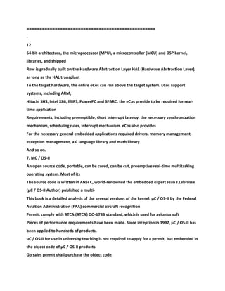


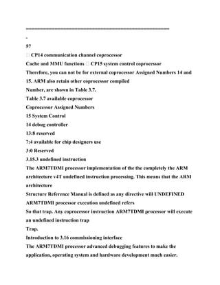
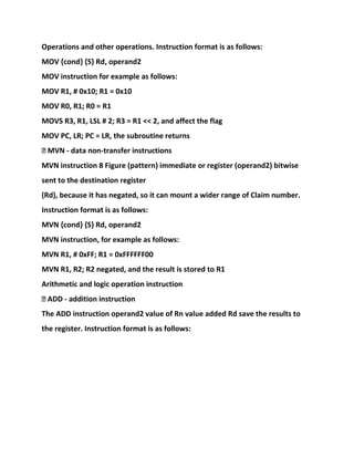
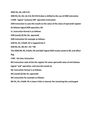
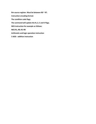
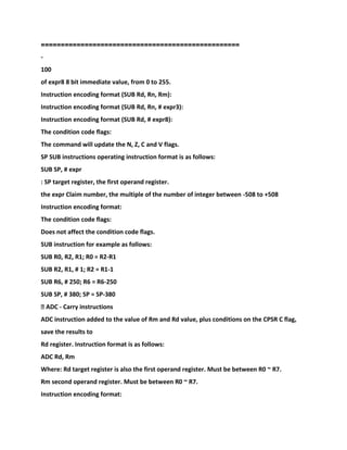
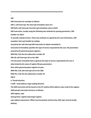
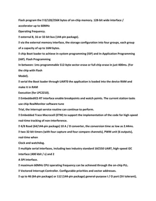
![==================================================
-
30
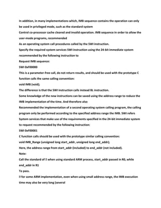
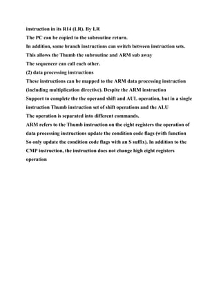
32 - bit ALU
CLK
CLKEN
CFGBIGEND
nFIQ
nRESET
ABORT
TRANS [1:0]
PROT [1:0]
SIZE [1:0]
WRITE
LOCK
WDATA [31:0] RDATA [31:0]
ADDR [31:0]
Address register
Scan debug
Control
Write data register
CP handshake
CP control
DBG input
DBG output
Instruction decoder
And
Control logic
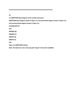
Register set](https://image.slidesharecdn.com/armembeddedsystemessentialszlg-230111081204-4bc9ad56/85/ARM-Embedded-System-Essentials-ZLG-docx-106-320.jpg)
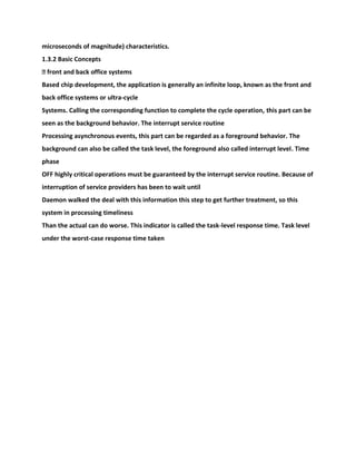
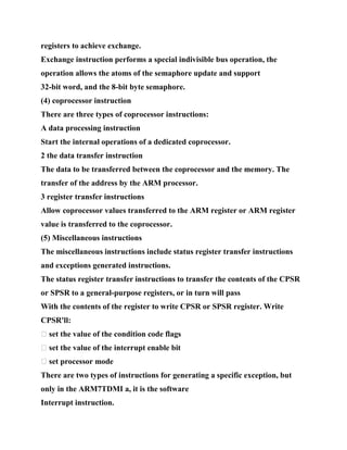
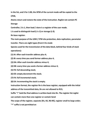
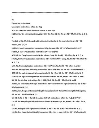
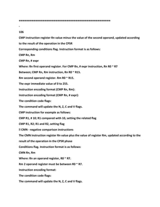
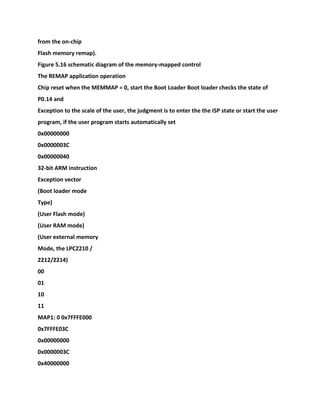
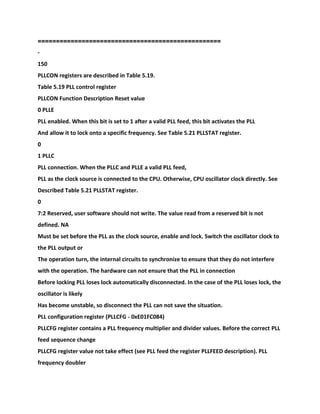
![31 × 32 - bit register
(6 Status Register)
Address the increase
Barrel shifter
The instruction pipeline read data register
Thumb instruction decoder
Multiplier
nIRQ
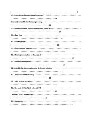
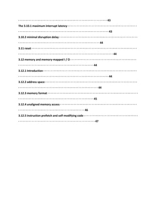
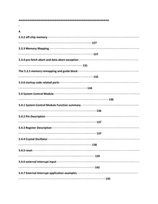
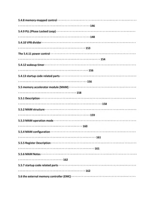
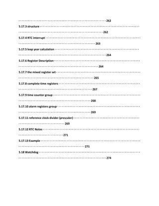
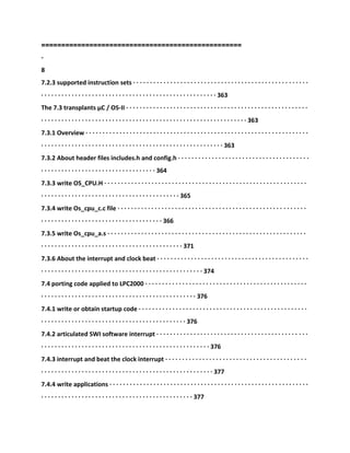
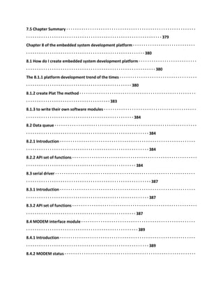
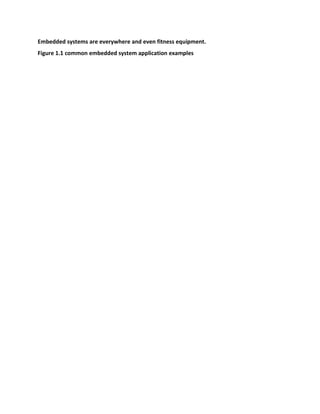
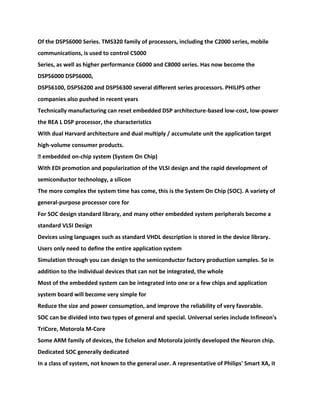
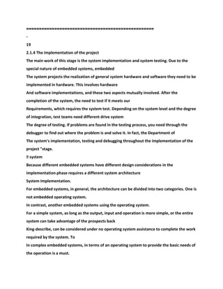
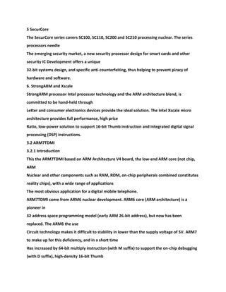
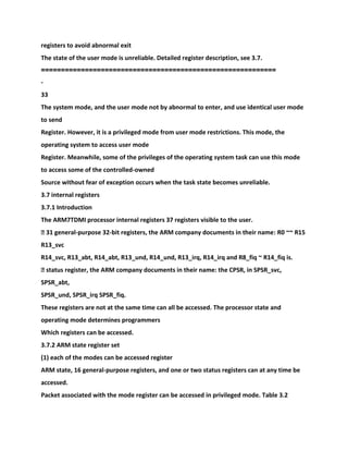
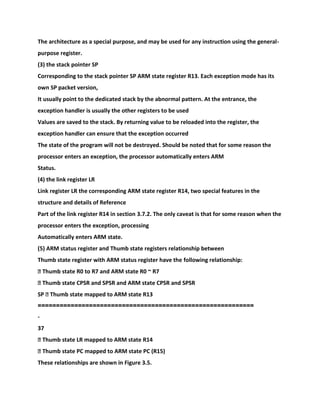
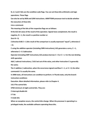
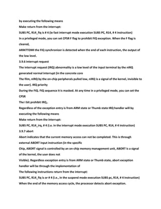
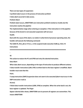
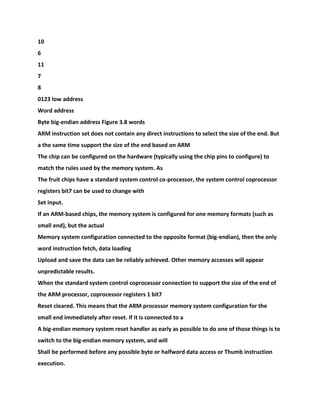
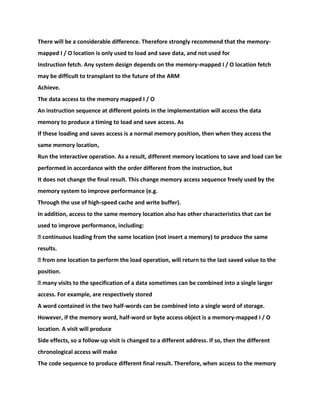
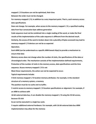
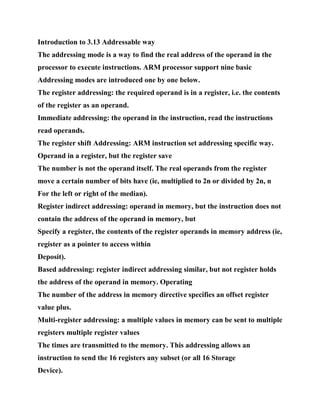
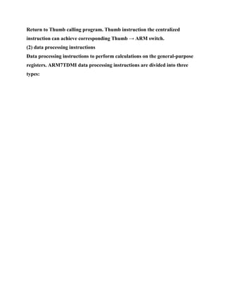
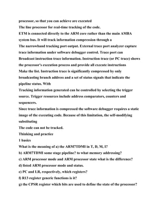
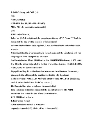
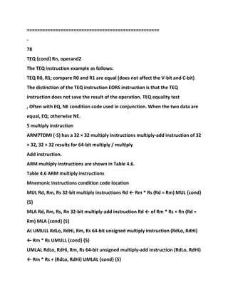
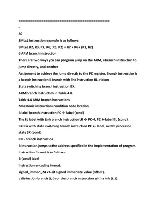
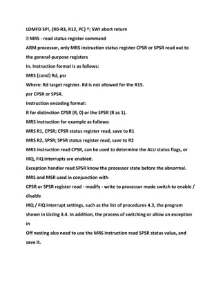
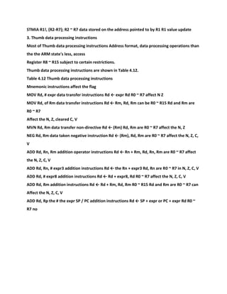
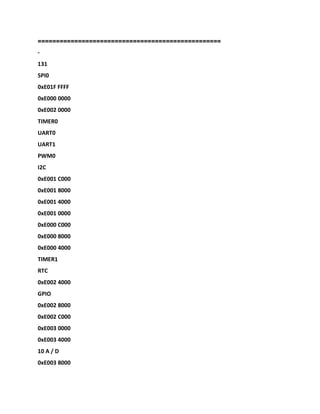
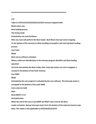
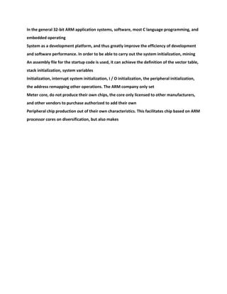
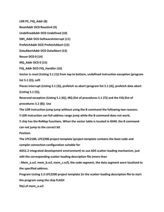
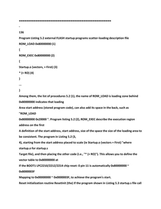
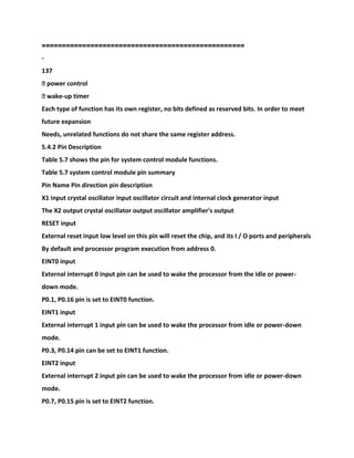
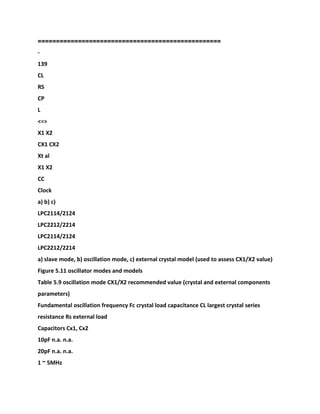
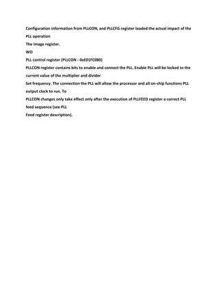
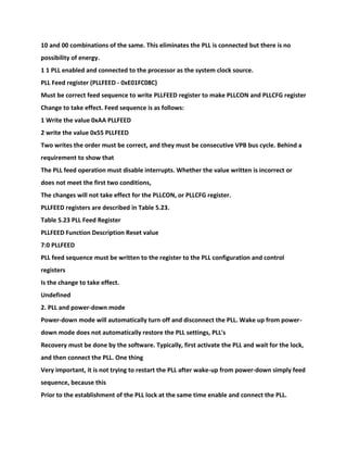
Figure 3.3 ARM7TDMI kernel
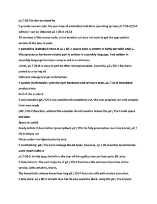
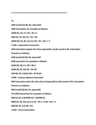
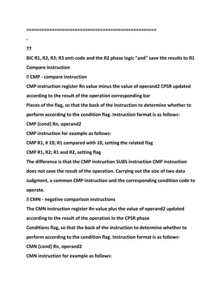
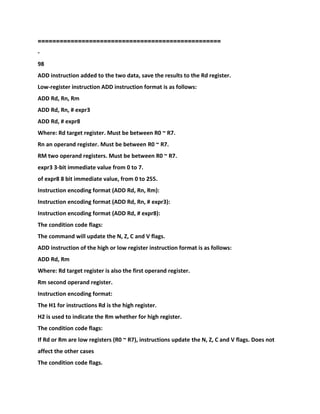
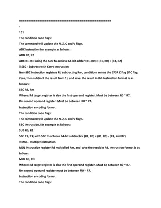
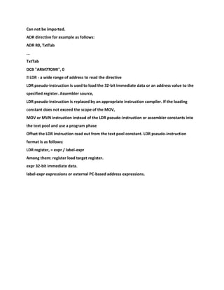
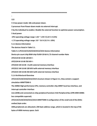
===========================================================
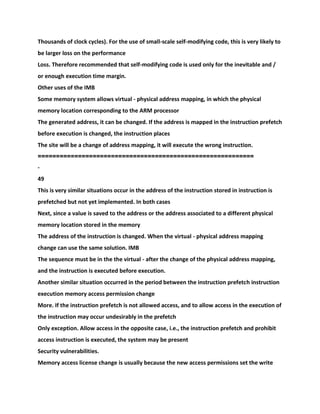
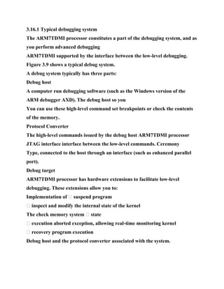
-
31
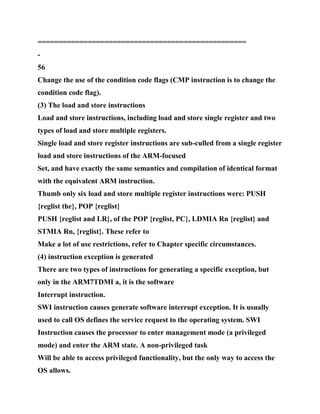
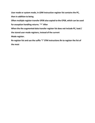
CPB
CPA
CPnI
CPTBIT
CPSEQ
CPnMREQ
CPnOPC
CPnTRANS
TRANS [1:0]
PROT [1:0]
SIZE [1:0]
WRITE
ABORT
RDATA [31:0]
WDATA [31:0]
ADDR [31:0]
DBGTDO](https://image.slidesharecdn.com/armembeddedsystemessentialszlg-230111081204-4bc9ad56/85/ARM-Embedded-System-Essentials-ZLG-docx-107-320.jpg)
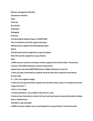
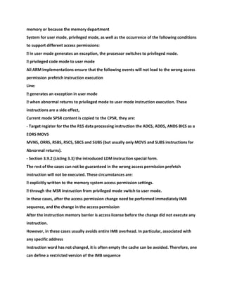
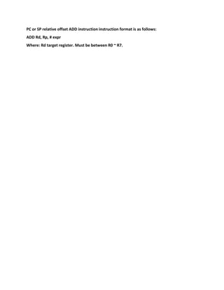
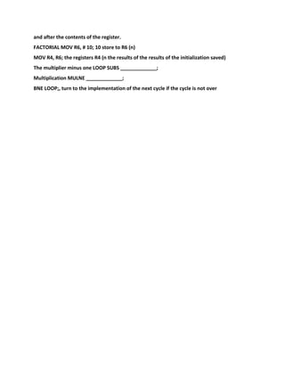
![DBGnTDOEN
DBGnTRST
DBGTDI
DBGTMS
DBGTCKEN
DBGCOMMTX
DBGCOMMRX
DBGRNG [0]
DBGRNG [1]
DBGEN
DBGEXT [0]
DBGEXT [1]
DBGnEXEC
DBGACK
DBGBREAK
DBGRQ
LOCK
CFGBIGEND
nRESET
nFIQ
nIRQ
CLKEN
CLK
DBGINSTRVALID
DMORE ARM7TDMI-S
Synchronization
EmbededICE-RT
Scan Debug Access Port
Memory interface](https://image.slidesharecdn.com/armembeddedsystemessentialszlg-230111081204-4bc9ad56/85/ARM-Embedded-System-Essentials-ZLG-docx-108-320.jpg)
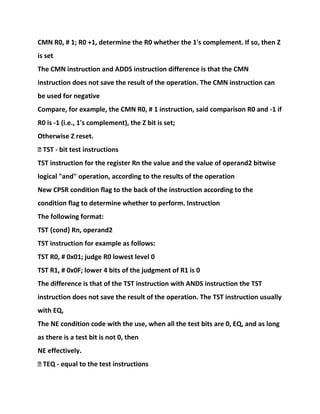
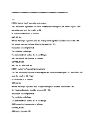
![-
34
Assembler program in ADS1.2 directly support these names, but pay attention to the a1-a4,
v1 to v8 must use the lowercase letters. Details, see Reference [1].
(2) Average of general purpose registers
In assembly language register R0 ~ R13 to save data or address values of the general-purpose
registers. Which registers R0 ~ R7
The ungrouped register. This means that for any processor mode, each of them
corresponding to the same 32-bit
Physical register. They are completely general purpose register is not architecture as a special
purpose, and may be used for any
Using the general purpose registers of the instruction.
Register R8 ~ R14 group register. Their corresponding physical register depends on the
current processor mode. A few
Almost all instruction allows the use of general-purpose registers allows the use of packet
register.
Registers R8 ~ R12 have the physical registers of the two packets. One for outside the FIQ
mode registers mode
(R8 to R12), the other for the FIQ mode (R8_fiq ~ R12_fiq).
Register R8 ~ R12 ARM architecture without a specific purpose. But for those who use only R8
~ R14
These registers are sufficient to handle simple interrupt FIQ used alone can achieve the fast
interrupt processing.
The registers R13 and R14, respectively, the physical registers of the six packets. One for the
user and system mode, the remaining five
And one each for the five kinds of abnormal patterns.
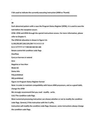
(3) the stack pointer R13
The registers R13 usually as the stack pointer (SP). ARM instruction set, which the use is not
in a special way.](https://image.slidesharecdn.com/armembeddedsystemessentialszlg-230111081204-4bc9ad56/85/ARM-Embedded-System-Essentials-ZLG-docx-114-320.jpg)
![Read general limitations of the program counter
Read the instructions on the R15 to read no more than any restrictions on the R15, the value
is the address of the instruction plus
8 bytes. Units, the results of the bit ARM instructions are always word [1:0] is always 0.
Read the PC is mainly used on the the nearby instructions and data quickly, and location-
independent addressing
The program has nothing to do with the location of the transfer.
When using STR or STM instructions save R15, an exception to the above rule. These
instructions can be the finger
Address plus 8 bytes saved (and other instructions to read R15) or the instruction plus 12
bytes (the future can also own address
Appearing on other data). Offset 8 or 12 (or other value) depends on ARM implementations
(ie,
Chip-related). For a specific chip, it is a constant. STR and STM instructions are not so
portable.
Since this exception, it is best to avoid using the STR and STM instructions to save R15. If it is
difficult to do, then should
Suitable instruction sequence offset used to determine the current use of the chip used in the
program. For example, using the program list
The the 3.2 instruction sequence shown in this offset stored in R0.
Program Listing 3.2 offset concrete chip storage PC
SUB R1, PC, # 4; R1 = following STR instruction address
STR PC, [R0]; Save the the STR instruction address + offset
LDR R0, [R0]; then reinstall
SUB R0, R0, R1; offset
General limit to write the program counter
R15 instruction does not exceed any limit its use when executing a write, write R15 normal
results
Value as an address of the instruction, the program from this address to continue (equivalent](https://image.slidesharecdn.com/armembeddedsystemessentialszlg-230111081204-4bc9ad56/85/ARM-Embedded-System-Essentials-ZLG-docx-117-320.jpg)
![to perform an unconditional jump).
ARM instruction word boundary, so write the value of R15 bit [1:] usually 0b00. The specific
rules depends
The used version of the structure:
� V3 version and the following versions of the ARM architecture, write the value of R15 bit
[1:0] are ignored, so the instruction real
The International destination address (the value written to R15) and 0xFFFFFFFC phase.
� structure V4 version in ARM (ARM7TDMI based on the V4 version) and above, write the
value of R15 bit [1:0]
Must be 0b00. If not, the results will be unpredictable.
(6) The program status register
All modes share a program status register (CPSR), abnormal pattern, a register program
status
Save register (SPSR) can be accessed. Each exception has its own SPSR, save it into the
abnormal CPSR
The current value of it to restore the CPSR abnormal exit. The description of the program
status register, see 3.8.
3.7.3 Thumb state register set
(1) each of the modes can be accessed register
Thumb state register set is a subset of the ARM state set. Programmers can directly access:
� 8 general purpose registers R0 to R7
===========================================================
-
36
� PC
� stack pointer (SP)
� connection Register (LR)
� CPSR (conditional access)
SP and LR for each privileged mode packet. Thumb registers detailed in Table 3.3.](https://image.slidesharecdn.com/armembeddedsystemessentialszlg-230111081204-4bc9ad56/85/ARM-Embedded-System-Essentials-ZLG-docx-118-320.jpg)
![Table 3.3 Thumb state mode register
Register each mode access register
Category
Register in assembly
In the name of the user system management abort undefined interrupt fast interrupt
R0 (a1) R0
R1 (a2) R1
R2 (a3) R2
R3 (a4) R3
R4 (v1) R4
R5 (v2) R5
R6 (v3) R6
R7 (v4, WR) R7
SP R13 R13_svc R13_abt R13_und R13_irq R13_fiq
LR R14 R14_svc R14_abt R14_und R14_irq R14_fiq
General-purpose registers and program counter
PC R15
Status register
Register
CPSR CPSR
Note: brackets ATPCS register naming RN assembler directive to register multiple names, you
can use. Among them,
Assembler ADS1.2 the direct support for these names, but note a1-a4 v1 ~~ v4 must be in
lowercase. Details, refer to Reference [1].
(2) Average of general purpose registers
Register R0 ~ R7 to save data or address values of the general-purpose registers in assembly
language. For any processor module
Formula, each of them corresponding to the same 32-bit physical registers. They are
completely general-purpose registers, will not be](https://image.slidesharecdn.com/armembeddedsystemessentialszlg-230111081204-4bc9ad56/85/ARM-Embedded-System-Essentials-ZLG-docx-119-320.jpg)
![Interrupt Disable bit
I and F bits are the interrupt disable bits:
� When I bit is set, IRQ interrupts are disabled
� when the F bit, FIQ interrupts are disabled
===========================================================
-
39
T bit
T bit reflects the state are operating:
� when the T bit, the processor is in Thumb state run
� when the T bit is cleared, the processor is ARM state run
Warning: Do not force changes in the T bit in the CPSR register. If you do this, the processor
will enter an inability
Unknown state.
Mode bit
M4, M3, M2, M1 and M0 bits (M [4:0]) are the mode bits. These bits determine the
processor's operating mode, see Table
3.4. Not all of the combinations of the mode bits define a valid processor mode, so be careful
not to use the table does not
The combinations listed.
Table 3.4 CPSR mode bits value
M [4:0] the pattern visible Thumb state registers visible ARM state register
The 10,000 users R0 to R7, SP, LR, PC, CPSR R0 to R14, the PC, CPSR
10001 fast interrupt R0 ~ R7, SP_fiq, LR_fiq, PC, CPSR,
SPSR_fiq
R0 ~ R7, R8_fiq ~ R14_fiq, PC, CPSR,
SPSR_fiq
10010 interrupt R0 ~ R7, SP_irq, LR_irq, PC, CPSR,
SPSR_fiq](https://image.slidesharecdn.com/armembeddedsystemessentialszlg-230111081204-4bc9ad56/85/ARM-Embedded-System-Essentials-ZLG-docx-125-320.jpg)
![R0 ~ R12, R13_irq, R14_irq, PC, CPSR,
SPSR_irq
10011 management R0 ~ R7, SP_svc, LR_svc, PC, CPSR,
SPSR_svc
R0 ~ R12, R13_svc, R14_svc, PC, CPSR,
SPSR_svc
10111 abort R0 ~ R7, SP_abt, LR_abt, PC, CPSR,
SPSR_abt
R0 ~ R12, R13_abt, R14_abt, PC, CPSR,
SPSR_abt
11011 undefined R0 to R7, SP_und LR_und, PC, CPSR,
SPSR_und
R0 ~ R12, R13_und, R14_und, PC, CPSR,
SPSR_und
11111 system R0 to R7, SP, LR, PC, CPSR R0 to R14, the PC, CPSR
Note: If you write illegal values M [4:0], the processor will enter an unrecoverable mode.
3.8.4 reserved bits
Reserved bits in the CPSR are reserved for future use. Make sure when to change the the
CPSR flag and control bits when not changed
These reserved bits. Also, make sure your program does not rely on reserved bits containing
specific values, because the future of the processor may
These bits are set to 1 or 0.
3.9 abnormal
3.9.1 Introduction
Normal program flow is temporarily suspended, the processor enters exception mode. For
example, in response to an interrupt from a peripheral.
Before handling exceptions, ARM7TDMI core save the current state of the processor, so that
when the end of the handler can recover
Repeatedly executed the original program.](https://image.slidesharecdn.com/armembeddedsystemessentialszlg-230111081204-4bc9ad56/85/ARM-Embedded-System-Essentials-ZLG-docx-126-320.jpg)
![Note: ARM7TDMI processor completely follow ARM architecture v4T, you can capture all
Category undefined instruction bits
Format.
Instructions to prevent failure, capture the processor to execute the following command:
MOVS PC, R14_und (ie undefined mode execution MOVS PC, R14 instruction)
This action to restore the PC and CPSR, and returns to the instruction after the undefined
instruction.
The undefined instruction more detailed information please refer to reference [2].
3.9.10 exception vector
Table 3.6 shows the exception vector address. , I, and F represents the previous value in the
table.
Table 3.6 exception vector
Address abnormal entry mode to enter when I state into the state of the F
0x00000000 reset management are prohibited
0x00000004 undefined instruction is undefined I F
0x00000008 software interrupt management prohibited F
=================
==========================================
-
43
Connected to the table
Address abnormal entry mode to enter when I state into the state of the F
And 0x0000000C abort abort (prefetch) I F
0x00000010 abort abort (data) I F
0x00000014 Reserved -
0x00000018 IRQ interrupts disabled F
The 0x0000001C FIQ fast interrupt prohibited prohibition
3.9.11 Exception Priorities
When multiple exceptions occur simultaneously, a fixed priority system determines the order
in which they are processed:](https://image.slidesharecdn.com/armembeddedsystemessentialszlg-230111081204-4bc9ad56/85/ARM-Embedded-System-Essentials-ZLG-docx-133-320.jpg)
![Zero Wait.
� Texc, data abort the time of the entrance. Texc for three cycles (determined by the kernel).
� Tfiq the FIQ entrance time. Tfiq for two cycles (determined by the kernel).
Therefore, the total delay time for the 27 cycles, the system uses a 40 MHz processor clock,
slightly less than 0.7 microseconds.
Located 0x1c at the instruction after the end of this time, ARM7TDMI execution.
Largest IRQ delay time is similar, but must take into consideration such a fact, i.e. a higher
priority FIQ
When the application of the FIQ and IRQ, IRQ delay to FIQ handlers to allow the IRQ interrupt
when handling (you may need
Corresponding interrupt controller). IRQ delay time should be correspondingly increased.
======================================
=====================
-
44
3.10.2 Minimum interrupt latency
FIQ or IRQ minimum interrupt latency request through the the time synchronizer plus
Tsyncmin Tfiq (4 processing
Control cycle).
3.11 Reset
Other sources of reset when nRESET signal is pulled low (usually external reset pin level
changes and chip change
Core signal), the ARM7TDMI processor abandon the instruction being executed.
NRESET signal goes high again, ARM processor performs the following actions:
Forced M [4:0] becomes b10011 (management model)
Set CPSR I and F bits
3. Clears the T bit in the CPSR
4. Force the PC began to fetch the next instruction from address 0x00.
5. Return to ARM state and resume execution
After reset, all register values except the PC and CPSR are not OK.](https://image.slidesharecdn.com/armembeddedsystemessentialszlg-230111081204-4bc9ad56/85/ARM-Embedded-System-Essentials-ZLG-docx-135-320.jpg)
![Note: The load and save memory format of the rules means that the word is not influenced
by the size of the end of the configuration. Therefore, not
Can save a word to change the memory format, and then reload the saved words so that the
order of the bytes of the word among the flip.
In general, change the the ARM processor configuration memory format memory system
does not make it different from the connection
What is the use of an additional structure defined operation, because to do so results and will
not produce. Therefore typically only in the reset
Change the configuration of the memory format so that it matches the memory system
memory format.
3.12.4 unaligned memory access
ARM the structure normally expect all memory accesses are reasonable alignment.
Specifically word accesses address usually
Word aligned halfword access address halfword aligned. Not memory access is called the
non-aligned in this manner
Aligned memory access.
Non-aligned instruction fetch
If the ARM state will be a non-word aligned address to write R15, the result is usually
unpredictable. If the Thumb
State to a non-aligned halfword address written to R15, address bits bit [0] is usually ignored
(see 3.7 and Chapter 4 each
A detailed description of the specific instruction). Results valid code from R15 in ARM state
read out the value of bit [1:0] 0 in
Bit0 of the Thumb state readout R15 value is 0.
When the the provisions ignore these bit, ARM implementation does not require instruction
fetch bit is cleared. Can be written to R15
The value of the change is sent to the memory, ARM or Thumb instruction fetch request
address bits are ignored bit [1:0]
Or bit [0].](https://image.slidesharecdn.com/armembeddedsystemessentialszlg-230111081204-4bc9ad56/85/ARM-Embedded-System-Essentials-ZLG-docx-141-320.jpg)
![Unaligned data access
Action one unaligned access load / save instructions will appear the following definitions:
� unpredictable
� access is not aligned low address bits are ignored. This means that when the half-word
access using Equation (ADDRESS AND
0xFFFFFFFE), and when the word access to use formula (address AND 0xFFFFFFFC).
� access is not aligned low address bits are ignored memory access control devices, and then
use these low address bits
The upload data cycle (the action is only applicable to LDR and SWP instruction).
Which of the three options suitable for load / save instruction depends on the instruction
(see Chapter 4).
===========================================================
-
47
Be sent to the address memory the ARM requirements will result in non-aligned low address
bits are cleared. Can be installed
Load / save instruction calculates an address does not change, is sent to the memory, and the
half-word access or word access request memory
The system ignores address bit bit [0] or bit [1:0].
3.12.5 prefetch instruction and self-modifying code
Many ARM to achieve the first execution of an instruction has not yet completed the
instruction fetched from memory. This action is called
Instruction prefetch. Instruction prefetch not actual execution instruction. Instruction did not
subsequently perform two typical situation:
� When an exception occurs, the current instruction is finished, all prefetch instructions are
discarded, execution of instructions from abnormal
Vector begins.
� When the jump occurred, the prefetched instruction after the branch instruction will be
discarded.](https://image.slidesharecdn.com/armembeddedsystemessentialszlg-230111081204-4bc9ad56/85/ARM-Embedded-System-Essentials-ZLG-docx-142-320.jpg)


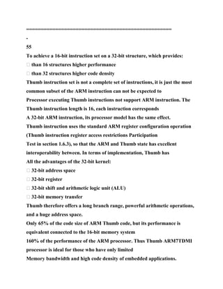
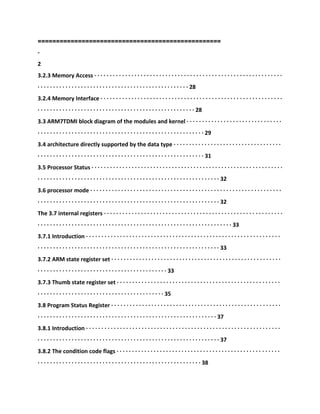
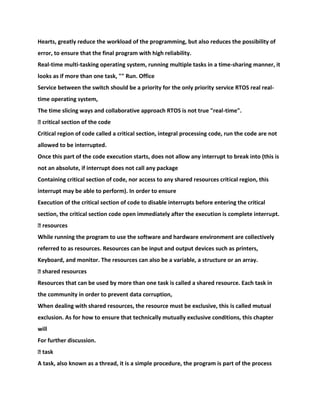
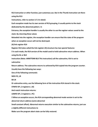
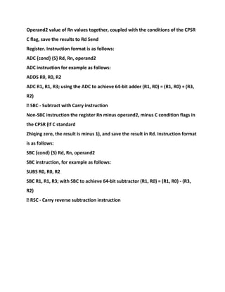
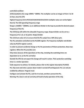
![EmbeddedICE-RT
DBGRNG [1:0]
DBGACK
DBGBREAK
DBGCOMMTX
DBGCOMMRX
DBGRQ
DBGEXT [1:0]
DBGEN
TAP
DBGTCKEN
DBGTMS
DBGTDI
DBGTDO
DBG nT RT S
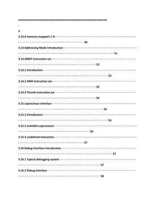
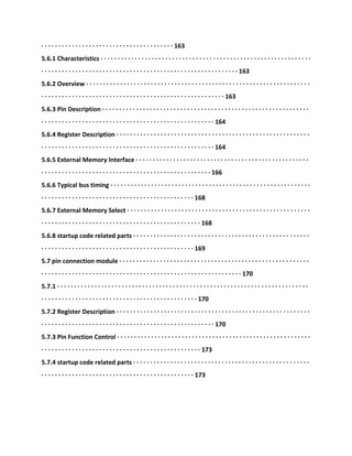
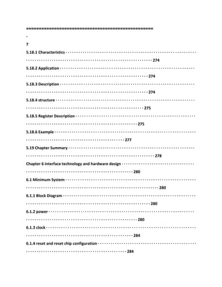
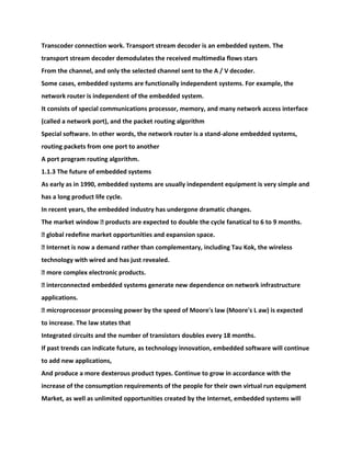
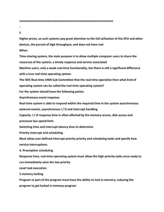
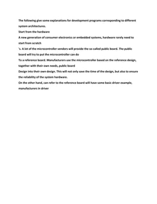
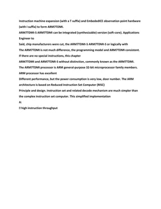
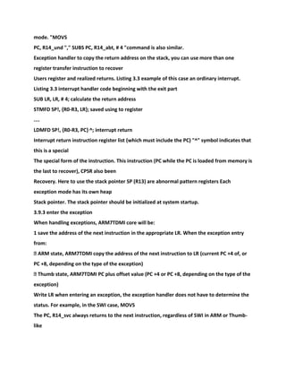
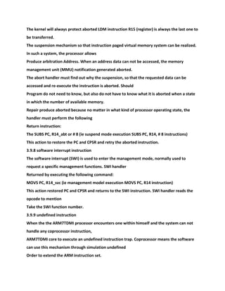
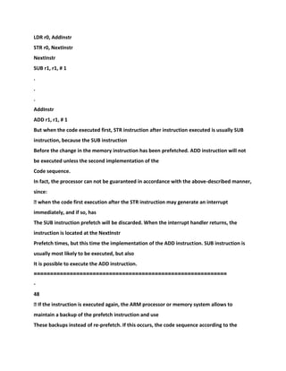
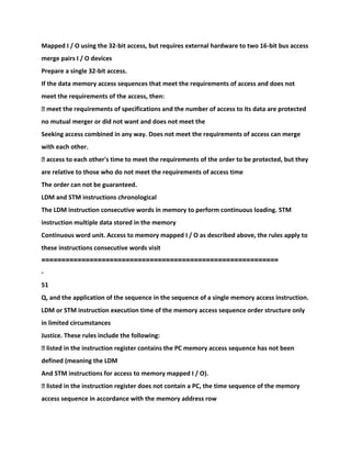
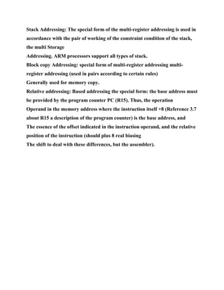
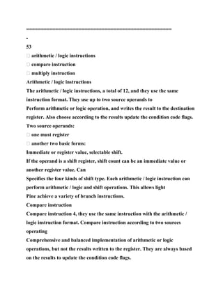
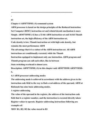
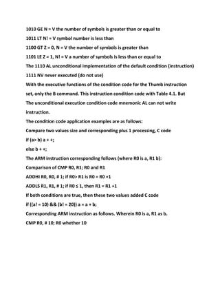
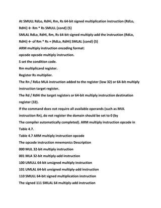
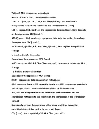
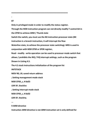
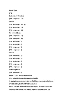
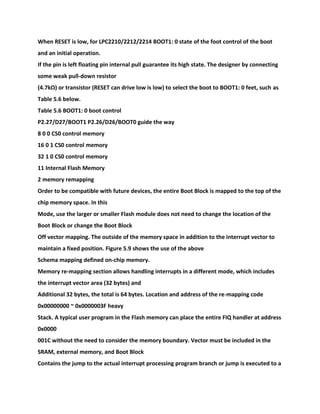
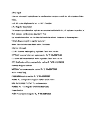
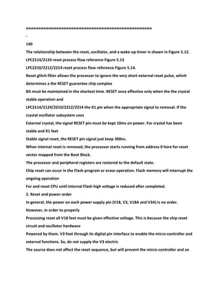
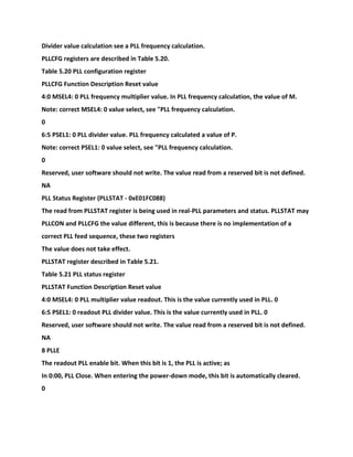
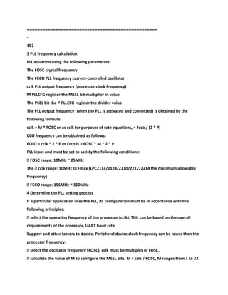
Figure 3.10 ARM7TDMI core TAP controller and the EmbeddedICE-RT
macrocell](https://image.slidesharecdn.com/armembeddedsystemessentialszlg-230111081204-4bc9ad56/85/ARM-Embedded-System-Essentials-ZLG-docx-175-320.jpg)


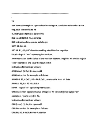
![==================================================
-
62
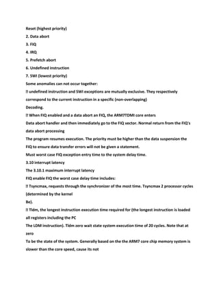
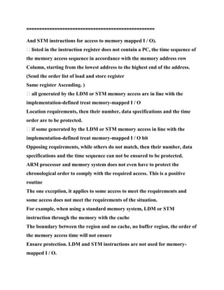
The various shift operation is shown in Figure 4.1.
(A) LSL shift operation
(B) LSR shift operation
(C) ASR shift operation
(D) ROR shift operation
(E) RRX shift operation
Figure 4.1 shift operation schematic diagram
Register indirect addressing
Address register indirect addressing instruction code given a number of
general-purpose registers, and the number of operations required to save in
Register specifies the address of the storage unit, i.e., the register is the
address of the operand pointer. For example, register indirect addressing
instruction
Follows:
LDR R1, [R2]; R2 pointing to a memory cell data is read out, stored in the R1
SWP R1, R1, [R2]; the exchange of the value of the register R1, and R2
specify the contents of the storage unit
5 Based addressing
Based addressing is the sum of the contents of the base register and
instruction given offset formed operand effective
Address. Based addressing is used to access near the base address of the
storage unit, commonly used in the look-up table, an array of operating
features register access
And so on. Based addressing instruction for example as follows:](https://image.slidesharecdn.com/armembeddedsystemessentialszlg-230111081204-4bc9ad56/85/ARM-Embedded-System-Essentials-ZLG-docx-183-320.jpg)
![LDR R2, [R3, # 0x0C]; read R3 +0 x0C address the contents of the storage
unit, into the R2
STR R1, [R0, # -4]!; First R0 = R0-4, then the value of R1 Storage to save
specified to R0
; Storage unit
LDR R1, [R0, R3, LSL # 1]; readout R0 + R3 × 2 address the contents of the
storage unit, memory
; Into R1
Register addressing
Multi-register addressing that one can send several register values, allow an
instruction to send the 16 registers any child
Set or register. Examples of multi-register addressing instruction as follows:
LDMIA R1!, {R2-R7, R12}; the R1 point unit data read out to R2 ~~ R7, R12
; (R1 automatically incremented by 1)
STMIA R0!, {R2-R7, R12}; register R2 ~ R7, R12 value of saved storage
pointed to R0
; Unit (R0 automatically incremented by 1)
0
0
C](https://image.slidesharecdn.com/armembeddedsystemessentialszlg-230111081204-4bc9ad56/85/ARM-Embedded-System-Essentials-ZLG-docx-184-320.jpg)


![===================================================
-
65
Must be written {<cond>} instruction execution condition is optional. If writing
is to use the default condition AL (unconditional
Execution).
opcode instruction mnemonic, LDR, STR.
cond execution condition, such as EQ, NE.
S would not affect the value of the CPSR, writing affect the CPSR.
Rd target register.
Rn an operand register.
operand2 two operands.
The instruction format for example as follows:
LDR R0, [R1]; read the R1 address of the memory cell content, the execution
condition Al
The BEQ DATAEVEN; branch instruction execution condition EQ, ie equal, jump
; To DATAEVEN
ADDS R1, R1, # 1; addition instruction, R1 +1 => R1, affect the CPSR (S)
SUBNES R1, R1, # 0x10; conditional execution subtraction operation (NE), R1-
0x10 => R1, impact
; CPSR register (S)
The first two operands
ARM instruction, the flexibility to use two operands to improve code efficiency.
Two operand forms such as
Follows:](https://image.slidesharecdn.com/armembeddedsystemessentialszlg-230111081204-4bc9ad56/85/ARM-Embedded-System-Essentials-ZLG-docx-192-320.jpg)
![� # immed_8r - constant expression
The constant must correspond to 8-bit bitmap (pattern), that the constant is
shifted by an 8-bit constant cycle even bits obtained.
Legitimate constants: 0x3FC (0xFF << 2), 0, 0xF0000000 (0xF0 << 24), 200 (0xC8),
0xF0000001 (0x1F << 28).
Illegal constant: 0x1FE 511,0 xFFFF, 0x1010, 0xF0000010.
The constant expressions application example:
MOV R0, # 1; R0 = 1
AND R1, R2, # 0x0F; R2 and 0x0F save the result in R1
LDR R0, [R1], # -4; read the R1 address the memory unit contents, and R1 = R1-4
� Rm - register way
In the mode register, the operand is the register values.
The register mode application example:
SUB R1, R1, R2; R1-R2 => R1
MOV PC, R0; PC = R0, the program jumps to the specified address
LDR R0, [R1],-R2; read the memory cell contents in the R1 address and stored in
R0, R1 = R1-R2
� Rm, shift - register shift mode.
The results of the shift register as the operand, the Rm value saved unchanged,
the shifting method is as follows:
ASR # n n-bit arithmetic shift right (1 ≤ n ≤ 32).
Logical Shift Left LSL # n n-bit (1 ≤ n ≤ 31).
LSR # n logical right by n bits (1 ≤ n ≤ 32).
Rotate Right ROR # n n-bit (1 ≤ n ≤ 31).
The RRX band extended rotate right one.](https://image.slidesharecdn.com/armembeddedsystemessentialszlg-230111081204-4bc9ad56/85/ARM-Embedded-System-Essentials-ZLG-docx-193-320.jpg)

![===================================================
-
67
CMPNE R1, # 20; If R0 10 R1 is 20
ADDNE R0, R0, R1; If R0 10 and R1 is not 20, the instruction execution, R0 = R0 +
R1
3 ARM memory access instructions
ARM processors are load / store architecture typical RISC processor, the
memory access can only use plus
Load and store instructions. ARM load / store instructions to achieve word, half-
word unsigned / signed byte operations; multi Send
Register load / store instruction is an instruction to load / store multiple
registers, greatly improving efficiency; SWP instruction
Is a register and the memory content switching instruction, and can be used for
the semaphore operation. The ARM processor is a von Neumann deposit
Storage structure, program space, RAM space and I / O mapping space unified
addressing, in addition to the operation of RAM on peripheral IO,
Program data access to be performed by load / store instructions.
ARM memory access instructions are shown in Table 4.2.
Table 4.2 ARM memory access instructions
Mnemonic instructions condition code location
LDR Rd, addressing word data is loaded Rd ← [addressing] addressing index LDR
{cond}
LDRB Rd, addressing load unsigned byte data Rd ← [addressing] addressing
index LDR {cond} B](https://image.slidesharecdn.com/armembeddedsystemessentialszlg-230111081204-4bc9ad56/85/ARM-Embedded-System-Essentials-ZLG-docx-197-320.jpg)
![LDRT Rd, addressing user mode loaded word data Rd ← [addressing] addressing
index LDR {cond} T
LDRBT Rd, addressing user mode to load unsigned byte data Rd ← [addressing]
addressing index LDR {cond} BT
LDRH Rd, addressing load unsigned halfword data Rd ← [addressing] addressing
index LDR {cond} H
LDRSB Rd, addressing load signed byte data Rd ← [addressing] addressing index
LDR {cond} SB
LDRSH Rd, addressing load signed halfword data Rd ← [addressing] addressing
index LDR {cond} SH
STR Rd, addressing storage word data [addressing] ← Rd, addressing index STR
{cond}
STRB Rd, addressing storage byte data [addressing] ← Rd, addressing index STR
{cond}
STRT Rd, addressing the user-mode memory word data [addressing] ← Rd
addressing index STR {cond} T
STRBT Rd, addressing bytes of data stored in user mode [addressing] ← Rd,
addressing index STR {cond} BT
The STRH Rd, addressing storage halfword data [addressing] ← Rd, addressing
index STR {cond} H
LDM {mode} Rn {!} Reglist must multiple register load reglist must ← [Rn ...], Rn
writeback LDM {cond} {mode}
STM {mode} Rn {!} Reglist must register storage [Rn ...] ← reglist must Rn
writeback STM {cond} {mode}
SWP Rd, Rm, Rn register and memory word data exchange Rd ← [Rn], [Rn] ←](https://image.slidesharecdn.com/armembeddedsystemessentialszlg-230111081204-4bc9ad56/85/ARM-Embedded-System-Essentials-ZLG-docx-198-320.jpg)
![Rm (Rn ≠ Rd or Rm) SWP {cond}
SWPB Rd, Rm, the Rn registers and memory byte data exchange Rd ← [Rn], [Rn]
← Rm (Rn ≠ Rd or Rm) SWP {cond} B
� LDR and STR - load-store instruction
Load / store word and unsigned byte instructions
STR instructions store a single byte or word LDR instruction loaded from
memory to memory, a single byte or word
Into the register. LDR instruction is used to read data from memory into a
register; STR instruction is used to register the number of
It is saved to memory. Instruction format is as follows:
LDR {cond} {T} Rd, <address>; load the specified address on the data (words) in
Rd
STR {cond} {T} Rd, <address>; storing data (word) to the specified address
storage unit, to store
; Data in Rd
LDR {cond} B {T} Rd, <address>; loading byte data in Rd Rd lowest byte
; Effective, 24 cleared
STR {cond} B {T} Rd, <address>; storage bytes of data, the data to be stored in
Rd, minimum word
; Festival effective
Wherein, T is an optional suffix. Instruction T, then even if the processor is in a
privileged mode, the storage system will also visit](https://image.slidesharecdn.com/armembeddedsystemessentialszlg-230111081204-4bc9ad56/85/ARM-Embedded-System-Essentials-ZLG-docx-199-320.jpg)
![===================================================
-
68
Asked as the processor is in user mode. T in user mode invalid and can not be
used in conjunction with T with the former index offset.
Instruction encoding format:
I, P, U, W is used to distinguish the address mode (offset). I offset 12 0:00
legislation
I.e. number; I is 1, the offset amount for the shift registers. P denotes the pre /
post indexed, U table
Shown in plus / minus, W indicates write-back.
L is used to distinguish load (L is 1) or storage (L 0).
B for distinction byte at (B 1) or wordwise (B 0).
Rn base register.
Rd source / destination register.
LDR / STR instruction addressing is very flexible and consists of two parts, a part
of a base register, you can
Any one of general purpose registers; another portion as an address offset. The
address offset of the following formats:
(1) immediate. Claim number may be an unsigned values. This data can be
added to the base register, you can also
This value is subtracted from the base register. Instructions for example as
follows:
LDR R1, [R0, # 0x12]; R0 +0 x12 at the address of the data read out, save to R1
; (R0 values unchanged)](https://image.slidesharecdn.com/armembeddedsystemessentialszlg-230111081204-4bc9ad56/85/ARM-Embedded-System-Essentials-ZLG-docx-200-320.jpg)
![LDR R1, [R0, #-0x12]; the R0-0x12 at the address data is read out, saved to the
R1
; (R0 values unchanged)
LDR R1, [R0]; the R0 address data read-out, saved into R1 (zero-offset)
(2) register. Register values can be added to the base register can also be
subtracted from the base register number
Value. Instructions for example as follows:
LDR R1, [R0, R2]; R0 + R2 at the address data is read out, saved to R1 (the value
of R0 unchanged)
LDR R1, [R0,-R2]; R0-R2 at the address of the data read out, saved to R1 (the
value of R0 unchanged)
(3) registers, and the shift constant. The value can be added to the base register,
register shift can also be from the base register
Subtracted this value. Instructions for example as follows:
LDR R1, [R0, R2, LSL # 2]; R0 + R2 × 4 address data read out, save it to R1
; (R0, R2 value of the same)
LDR R1, [R0,-R2, LSL # 2]; R0-R2 × 4 at the address of the data read out, saved to
the R1
; (R0, R2 value of the same)
From addressing modes of address points, load / store instructions have the
following form:
(1) zero offset. The value of Rn as the address of the transmission data, i.e., the
address offset is 0. Instructions for example as follows:
LDR Rd, [Rn]
(2) before the index offset. In the data before transmission, the offset is added](https://image.slidesharecdn.com/armembeddedsystemessentialszlg-230111081204-4bc9ad56/85/ARM-Embedded-System-Essentials-ZLG-docx-201-320.jpg)
![to Rn, and the result as a transmission data storage
Address. If the use of the suffix "!", The result is written back into Rn, and Rn
the value does not allow for the R15. Instructions for example as follows:
LDR Rd, [Rn, # 0x04]!
LDR Rd, [Rn, #-0x04]
(3) procedures relative offset. Procedures relative offset to form another
version of the former index. The assembler PC register
Count offset, and the PC register as Rn generated before the index command.
Can not use the suffix "!" Instructions for example as follows:
LDR Rd, label; label program label, label must be within ± 4KB current
instruction
(4) after the index offset. The value of Rn is used as the storage address of the
transmission data. After the data transfer, the offset amount with Rn
Added together, the result is written back into Rn. Rn not allowed to R15.
Instructions for example as follows:](https://image.slidesharecdn.com/armembeddedsystemessentialszlg-230111081204-4bc9ad56/85/ARM-Embedded-System-Essentials-ZLG-docx-202-320.jpg)
![===================================================
-
69
LDR Rd, [Rn], # 0x04
Address alignment - in most cases, must be guaranteed for 32 to send the
address is 32-bit aligned.
Load / store word and unsigned byte instruction for example as follows:
Loaded R5 specified data (word address) and put it into R2 LDR R2, [R5];
STR R1, [R0, # 0x04]; storage unit of the data storage of R1 to R0 +0 x04, R0
values unchanged
LDRB R3, [R2], # 1; read the R2 address of the one-byte data, and save it into R3,
R2 = R2 +1
STRB R6, [R7]; R6, data is saved to the address specified by R7, only store one
byte
; Data
Load / store halfword and signed byte
Such LDR / STR instruction can load signed byte load signed halfword load /
store unsigned halfword. Offset
The amount of formats, addressing modes, and load / store word and unsigned
byte instructions. Instruction format is as follows:
LDR {cond} SB Rd, <address>; load the address specified on the data (signed
byte) in Rd
LDR {cond} SH Rd, <address>; load the address specified on the data (signed
half-word) in Rd
LDR {cond} H Rd, <address>; Load halfword data in Rd 16 Rd lowest effective](https://image.slidesharecdn.com/armembeddedsystemessentialszlg-230111081204-4bc9ad56/85/ARM-Embedded-System-Essentials-ZLG-docx-203-320.jpg)
![; High 16 cleared
STR {cond} H Rd, <address>; store halfword data you want to store the data in
Rd, a minimum of 16
Description: sign bit halfword / byte loaded is loaded with sign bit extended to
32; unsigned bit halfword loads
Zero-extended to 32 bits.
Instruction encoding format:
I, P, U, W is used to distinguish the address mode (offset). I offset 8 0:00
legislation
That number; I 1:00, offset offset register. P denotes the pre / post indexed, U
table
Shown in plus / minus, W indicates write-back.
L is used to distinguish load (L is 1) or storage (L 0).
S used to distinguish the symbolic access (S 1) and unsigned access (S 0).
H is used to distinguish halfword access (H 1) or byte access (H 0).
Rn base register.
Rd source / destination register.
Address alignment - the halfword address must be an even number. Non
halfword aligned halfword loads Rd contents will not
Rely; half-word aligned the halfword storage will allow the specified address 2
bytes of storage unreliable.
Load / store halfword and signed byte instruction example as follows:
LDRSB R1, [R0, R3]; R0 + R3 is the address of the byte data read out to the R1,
the high-order 24 bits are the sign bit
; Expansion](https://image.slidesharecdn.com/armembeddedsystemessentialszlg-230111081204-4bc9ad56/85/ARM-Embedded-System-Essentials-ZLG-docx-204-320.jpg)
![LDRSH R1, [R9]; R9 address on the half-word data is read out to the R1, 16 high
sign bit extension
LDRH R6, [R2], # 2; R2 half-word data on the address read out to the R6, high-
order 16-bit zero-extended.
; R2 = R2 +2
STRH R1, [R0, # 2]!; Save data R1 to R0 +2 address, stores only the lower 2 bytes
of data,](https://image.slidesharecdn.com/armembeddedsystemessentialszlg-230111081204-4bc9ad56/85/ARM-Embedded-System-Essentials-ZLG-docx-205-320.jpg)
![===================================================
-
71
Register of the low numbers, and will save the initial value of Rn; Rn load value
and stored value in the other cases unpredictable.
Address alignment - these instructions to ignore address bit [1:0].
Multiple register load / store instructions for example as follows:
LDMIA R0!, {R3-R9}; multi-word data loaded on the address pointed to by R0,
saved to R3 to R9 in
; R0 value update
STMIA R1!, {R3-R9}; R3 ~ R9 data stored in the address pointed to by R1 R1
value update
STMFD SP!, {R0-R7, LR}; site to save the R0 ~~ R7, LR stack
LDMFD SP!, {R0-R7, PC} ^; site restoration, exception handling return
During data replication, to set a good source data pointer and target pointer,
and then use the block copy addressing instruction
LDMIA / STMIA, LDMIB / STMIB, LDMDA / STMDA, LDMDB / STMDB read and
stored.
And stack operations, first set up the stack pointer, general use of the SP, and
then use the stack addressing instructions
STMFD / LDMFD, STMED / LDMED, STMFA / LDMFA STMEA / LDMEA stack
operations.
Multiple register transfer instruction is shown in Figure 4.2, where R1 is the
base register before the instruction execution, R1 'compared to
Instruction is executed after the base register.](https://image.slidesharecdn.com/armembeddedsystemessentialszlg-230111081204-4bc9ad56/85/ARM-Embedded-System-Essentials-ZLG-docx-209-320.jpg)

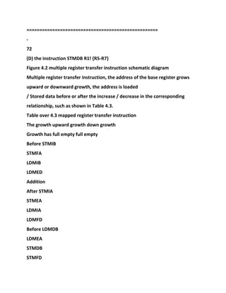
![Reduce
After LDMDA
LDMFA
STMDA
STMED
� SWP - exchange instruction register and memory
SWP instruction is used to read the contents of a memory unit (the unit address
on the register Rn) to a register
Rd, while another register Rm content is written to the memory unit. SWP
semaphore operations.
Instruction format is as follows:
SWP {cond} {B} Rd, Rm, [Rn]
Wherein, B is an optional suffix, if B, then the switch byte, otherwise exchanging
the 32-bit word; Rd for the data from the memory plus
Loaded into the register; data of Rm stored in the memory, and if Rm and Rn
same, compared to the registers and memory
Content to be exchanged; Rn want to exchange data memory address, Rn Rd
and Rm can not.
Instruction encoding format:
B is used to distinguish an unsigned byte (B 1) or word (B 0).
Rm source register.
Rd target register.
Rn base register.
SWP instruction for example as follows:
SWP R1, R1, [R0]; content to point to a memory cell the contents of R1 and R0 is](https://image.slidesharecdn.com/armembeddedsystemessentialszlg-230111081204-4bc9ad56/85/ARM-Embedded-System-Essentials-ZLG-docx-213-320.jpg)
![===================================================
-
73
SWPB R1, R2, [R0]; tolerance R0 points to a storage unit to read a byte of data
into R1 (high 24
;-Bit cleared), and R2 is written to the memory unit (lowest byte)
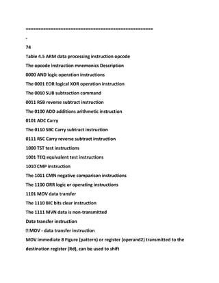
4 ARM data processing instruction
Data processing instructions can be broadly divided into three categories: data
transfer instruction (MOV, MVN), arithmetic logic operation instructions (such
as
ADD, SUB, AND), compare instructions (CMP, TST). Data processing instruction
operation only the contents of the register
For. All ARM data processing instruction can choose to use the S suffix, and
affect the status flags. Comparison instruction CMP, CMN,
TST and TEQ does not require suffix S, they will directly affect the status flags.
ARM data processing instructions are shown in Table 4.4.
Table 4.4 ARM data processing instruction
Mnemonic instructions condition code location
MOV Rd, operand2 data transmission Rd ← operand2 MOV {cond} {S}
The MVN Rd, operand2 data is non-transmission Rd ← (~ operand2) MVN
{cond} {S}
ADD Rd, Rn, operand2 addition instructions Rd ← Rn + operand2 the ADD
{cond} {S}
SUB Rd, Rn, operand2 subtraction instruction Rd ← Rn-operand2 SUB {cond} {S}
RSB Rd, Rn, operand2 the reverse subtraction Directive Rd ← operand2-Rn RSB](https://image.slidesharecdn.com/armembeddedsystemessentialszlg-230111081204-4bc9ad56/85/ARM-Embedded-System-Essentials-ZLG-docx-215-320.jpg)
![===================================================
-
81
BL DELAY
The branch instructions BL is limited within ± 32M byte address range of the
current instruction. The BL instruction for subroutine calls.
� BX - branch instruction with state switch
The BX instruction jumps to the address specified in the implementation of the
program in Rm, Rm the bit [0] to 1, jumps automatically to the CPSR
In logo T set target address of the code that is interpreted as Thumb code; Rm
the bit [0] is 0, then the jump
Automatically reset the flag in the CPSR T, that the code of the destination
address is interpreted as ARM code. Instruction format is as follows:
BX {cond} Rm
Instruction encoding format:
Rm destination address register.
State switching branch instruction BX for example as follows:
ADRL R0, ThumbFun +1
BX R0; jump to the designated address of the R0, and is switched in accordance
with the lowest bit of R0 at
; Processor state
7 ARM coprocessor instruction
ARM support the coprocessor operation, control coprocessor coprocessor
command.
ARM coprocessor instructions are shown in Table 4.9.](https://image.slidesharecdn.com/armembeddedsystemessentialszlg-230111081204-4bc9ad56/85/ARM-Embedded-System-Essentials-ZLG-docx-233-320.jpg)

![P, U, W is used to distinguish the address mode. P represents the before / after
index the U plus / minus, W
The write-back.
N data size (dependent on the co-processor).
LDC instruction for example as follows:
LDC p5, c2, [R2, # 4]; read R2 +4 points to the memory unit of the data sent to
the coprocessor
; P5 c2 register
LDC p6, c2, [R1]; R1 points to the memory unit is read data for delivery to the
coprocessor P6
; C2 register
� STC - coprocessor data write command
The STC instruction to coprocessor register data written to a contiguous
memory unit. Coprocessor data
The data transfer by the coprocessor to control the number of words
transmitted. Coprocessor can not successfully perform the operation, will
produce undetermined
Justice directive abort. Instruction format is as follows:
STC {cond} {L} coproc, CRd, <address>
Where: L Optional suffix, specified is long transfer.
coproc instruction coprocessor operation name. The standard named PN, n is 0
to 15.](https://image.slidesharecdn.com/armembeddedsystemessentialszlg-230111081204-4bc9ad56/85/ARM-Embedded-System-Essentials-ZLG-docx-238-320.jpg)
![===================================================
-
83
CRd as goal Storage coprocessor registers.
<Address> specified memory address.
Instruction encoding format:
cp_num coprocessor number.
8_bit_word_offset 8-bit immediate offset.
P, U, W is used to distinguish the address mode. P represents the before / after
index the U plus / minus, W
The write-back.
N data size (dependent on the co-processor).
STC instruction for example as follows:
STC p5, c1, [R0]
STC p5, c1, [R0, #-0x04]
� MCR - ARM register data transfer instructions to the coprocessor registers
MCR instruction ARM processor register data to the coprocessor registers. If the
co-processor is not
Able to successfully perform the operation, will produce undefined instruction
exception interrupt. Instruction format is as follows:
MCR {cond} coproc, opcode1, Rd, CRn, CRm {, opcode2}
Coprocessor name: coproc instruction operation. The standard named PN, n is 0
to 15.
specific opcode1 coprocessor opcode.
Rd as goal Storage coprocessor registers.](https://image.slidesharecdn.com/armembeddedsystemessentialszlg-230111081204-4bc9ad56/85/ARM-Embedded-System-Essentials-ZLG-docx-239-320.jpg)
![===================================================
-
85
MOV R0, # 12; soft interrupt call on the 12th
MOV R1, # 34; the Set subfunction number 34
SWI 0
The SWI exception interrupt handler, remove SWI immediate steps: First,
determine what caused the soft interrupt SWI
Instruction is the ARM instruction Thumb instruction, which can be get SPSR
access; then to get the SWI instruction
Address, which can be obtained by visiting the LR register; then read out the
instructions, decomposition immediate. As the program in Listing 4.2
Shows.
Program Listing 4.2 reads SWI immediate
T_bit EQU 0x20
SWI_Handler
STMFD SP!, {R0-R3, R12, LR}; site protection
MRS R0, SPSR; reads SPSR
STMFD SP!, {R0}; saved SPSR
TST R0, # T_bit; Testing T flag
LDRNEH R0, [LR, # -2]; if Thumb instructions, read the script (16)
Immediate BICNE R0, R0, # 0xFF00; obtain Thumb instruction 8
LDREQ R0, [LR, # -4]; ARM instruction to read the script (32)
24 BICEQ R0, R0, # 0xFF000000; made ARM instruction immediate
...](https://image.slidesharecdn.com/armembeddedsystemessentialszlg-230111081204-4bc9ad56/85/ARM-Embedded-System-Essentials-ZLG-docx-243-320.jpg)
![===================================================
-
86
Program Listing 4.3 enabled IRQ interrupt
ENABLE_IRQ
MRS R0, CPSR
BIC R0, R0, # 0x80
MSR CPSR_c, R0
MOV PC, LR
Disable IRQ interrupt the program list 4.4
DISABLE_IRQ
MRS R0 CPSR
ORR R0, R0, # 0x80
MSR CPSR_c, R0
MOV PC, LR
� MSR - write status register instruction
ARM processor, only MSR instructions can set the status register CPSR or the
SPSR. Instruction format
As follows:
MSR {cond} psr_fields, # immed_8r
MSR {cond} psr_fields, Rm
Among them: psr CPSR or SPSR.
fields specify a region of the transfer. The fields can be the following one or
more (letters must be lowercase):
c control the domain shielded byte (psr [7 ... 0]);](https://image.slidesharecdn.com/armembeddedsystemessentialszlg-230111081204-4bc9ad56/85/ARM-Embedded-System-Essentials-ZLG-docx-245-320.jpg)
![the x extension field mask byte (psr [15 ... 8]);
s status the domain shielded bytes (psr [23 ... 16]);
The f flag Domain mask byte (psr [31 ... 24]).
immed_8r to be sent to a status register domain specified immediate 8.
Rm be sent to the the status register domain specified data source register.
Instruction encoding format (operand immediate):
Instruction encoding format (operand register):
R for distinction CPSR (R, 0) or the SPSR (R as 1).
field_mask domain shielding.
rotate_imm immediate alignment.
8_bit_immediate 8-bit immediate data.
Rm operand register.
MSR instruction for example as follows:
MSR CPSR_c, # 0xD3; CPSR [7 ... 0] = 0xD3, switch to the management mode
MSR CPSR_cxsf, R3; CPSR = R3](https://image.slidesharecdn.com/armembeddedsystemessentialszlg-230111081204-4bc9ad56/85/ARM-Embedded-System-Essentials-ZLG-docx-246-320.jpg)

![===================================================
-
88
4.6 small range of program listings address the load
...
ADR R0, DISP_TAB; conversion table is loaded address
LDRB R1, [R0, R2]; using R2 as a parameter for look
...
DISP_TAB
DCB 0xC0, 0xF9, 0xA4, 0xB0, 0x99, 0x92, 0x82, 0xF8, 0x80, 0x90
� ADRL - the mid-range of the address read directive
The ADRL instruction will PC relative offset address value-based, or based on
the relative offset of the register address value read to register
Than ADR directive can be read by a wider address. Assembler source code,
ADRL directive is compiled
Replace two appropriate instruction. If two instructions can be used to achieve
ADRL pseudo-instruction, an error is generated, compiled
Fail. ADRL pseudo-instruction format is as follows:
ADRL {cond} register, expr
Among them: register load target register.
The Expr address expressions. When the non-word-aligned address value, the
range-64KB ~ 64KB between;
When the value of the address is word-aligned, the range-256KB ~ 256KB
between.
The ADRL directive for example as follows:](https://image.slidesharecdn.com/armembeddedsystemessentialszlg-230111081204-4bc9ad56/85/ARM-Embedded-System-Essentials-ZLG-docx-250-320.jpg)

![===================================================
-
89
Procedural relative offset LDR instruction read out from the text pool constant.
LDR pseudo-instruction format is as follows:
LDR {cond} register, = expr / label-expr
Among them: register load target register.
expr 32-bit immediate data.
label-expr expressions or external PC-based address expressions.
The directive of LADR example is as follows:
LDR R0, = 0x12345678; load 32-bit immediate data 0x12345678
LDR R0, = DATA_BUF +60; to load DATA_BUF address +60
...
LTORG; statement text pool
...
Directive LDR commonly used in the loaded chip peripheral features register
address (32-bit immediate data) in order to achieve a variety of control
System operation, such as the program shown in Listing 4.8.
Program list 4.8 to load the 32-bit immediate data
...
LDR R0, = IOPIN; the register IOPIN loaded GPIO address
LDR R1, [R0]; read IOPIN register value
...
LDR R0, = IOSET
LDR R1, = 0x00500500](https://image.slidesharecdn.com/armembeddedsystemessentialszlg-230111081204-4bc9ad56/85/ARM-Embedded-System-Essentials-ZLG-docx-253-320.jpg)
![STR R1, [R0]; IOSET = 0x00500500
...
Offset from the PC to the text pool must be less than 4KB.
Compared with the ARM instruction LDR LDR pseudo-instruction parameters "="
sign.
� NOP - No operation directive
The NOP directive in the assembly will be replaced by the empty operating in
ARM, for example, might refer to as "MOV R0, R0"
So. NOP directive format is as follows:
NOP
NOP can be used to delay the operation, as shown in the list of procedures 4.9.
Program list 4.9 software delay
...
DELAY1
NOP
NOP
NOP
SUBS R1, R1, # 1
BNE DELAY1](https://image.slidesharecdn.com/armembeddedsystemessentialszlg-230111081204-4bc9ad56/85/ARM-Embedded-System-Essentials-ZLG-docx-254-320.jpg)
![CODE32
ARM_CODE ADR R0, THUMB_CODE +1
BX R0; jump and switch the processor state
CODE16
THUMB_CODE
MOV R0, # 10; R0 = 10
MOV R1, # 20; R1 = 20
ADD R0, R1; R0 = R0 + R1
B.
END
The program first ARM state "ADR R0, THUMB_CODE +1" directive loading
Address THUMB_CODE order to R0 bit [0], so the use of "THUMB_CODE +1 such
BX is used to switch the processor state to Thumb state.
1. Thumb instruction set ARM instruction set difference
Thumb instruction set does not have a coprocessor instruction, the semaphore
instruction as well as access to the CPSR or SPSR instruction did not take
Plus instructions and 64-bit multiply instruction, the second operand and
instruction is limited; perform functions conditional branch instruction B
Can, other instructions are unconditional implementation; most Thumb data
processing instructions using address format. Thumb refers to
The difference between the set and the ARM instruction set is generally the
following points:
� branch instruction
Procedures relative shift, especially compared to the conditional jump jump
ARM code, there are more restrictions on the range,](https://image.slidesharecdn.com/armembeddedsystemessentialszlg-230111081204-4bc9ad56/85/ARM-Embedded-System-Essentials-ZLG-docx-256-320.jpg)
![Mnemonic instructions affect the flag
LDR Rd, [Rn, # immed_5 × 4] the loaded words Rd ← [Rn, of # immed_5 4] Rd, Rn R0 ~ R7 no
LDRH Rd, [Rn, # immed_5 × 2] load unsigned halfword data Rd ← [Rn, of # immed_5 × 2] Rd,
Rn R0 ~ R7 no
LDRB Rd, [Rn, # immed_5 × 1] load signed byte data Rd ← [Rn of # immed_5 × 1], Rd, Rn R0 ~
R7 no
STR Rd, [Rn, # immed_5 × 4] storing word data [Rn, # immed_5 × 4] ← Rd, Rd, Rn R0 ~ R7 no
STRH Rd, [Rn, # immed_5 × 2] storage signed halfword data [Rn of # immed_5 × 2] ← Rd, Rd,
Rn, R0 ~ R7 no
STRB Rd, [Rn, # immed_5 × 1] unsigned byte data storage [Rn, # immed_5 × 1] ← Rd, Rd, Rn,
R0 ~ R7 no
LDR Rd, [Rn, Rm] load word data Rd ← [Rn, Rm] Rd, Rn, Rm R0 ~ R7
LDRH Rd, [Rn, Rm] load signed halfword data Rd ← [Rn, Rm] Rd, Rn, Rm R0 ~ R7
LDRB Rd, [Rn, Rm] load signed byte data Rd ← [Rn, Rm, Rd, Rn, Rm R0 ~ R7 free
LDRSH Rd, [Rn, Rm] load signed halfword data Rd ← [Rn, Rm] Rd, Rn, Rm R0 ~ R7 no
LDRSB Rd, [Rn, Rm] load signed byte data Rd ← [Rn, Rm] Rd, Rn, Rm R0 ~ R7 no
STR Rd, [Rn, Rm] store word data [Rn, Rm] ← Rd, Rd, Rn, Rm R0 ~ R7
STRH Rd, [Rn, Rm] store unsigned halfword data [Rn, Rm ← Rd, Rd, Rn, Rm R0 ~ R7 None
STRB Rd, [Rn, Rm] the storage unsigned byte data [Rn, Rm ← Rd, Rd, Rn, Rm R0 ~ R7 None
LDR Rd, [PC, # immed_8 × 4] based on the the PC loaded word data Rd ← [the PC of #
immed_8 × 4] Rd R0 ~ R7 no
LDR Rd, label-based PC loaded word data Rd ← [label] Rd R0 ~ R7 no
LDR Rd, [SP, # immed_8 × 4] SP loaded word data Rd ← [SP of # immed_8 × 4] Rd R0 ~ R7 no
STR Rd, [SP, # immed_8 × 4] the the SP memory word data [SP, # immed_8 × 4] ← Rd Rd R0 ~
R7 no
LDMIA Rn {!}, Reglist multiple register load reglist must ← [Rn ...] Rn write-back (R0 ~ R7)
STMIA Rn {!}, Reglist multi-register storage [Rn ...] the ← in reglist, Rn write-back (R0 ~ R7)
PUSH {reglist [, LR]} register stack instruction [SP ...] ← reglist must [LR] SP writeback (R0 ~~
R7, LR) free](https://image.slidesharecdn.com/armembeddedsystemessentialszlg-230111081204-4bc9ad56/85/ARM-Embedded-System-Essentials-ZLG-docx-259-320.jpg)
![POP {reglist [, PC]} register the stack instruction reglist must [PC] ← [SP ...] SP write-back, etc.
(R0 ~~ R7, PC) free](https://image.slidesharecdn.com/armembeddedsystemessentialszlg-230111081204-4bc9ad56/85/ARM-Embedded-System-Essentials-ZLG-docx-260-320.jpg)
![==================================================
-
92
� LDR and STR - load / store instructions
Immediate offset LDR and STR instructions.
Memory address specified immediate offset to a register. Instruction format is as follows:
Load the specified address on the data (words) in Rd LDR Rd, [Rn, # immed_5 × 4];
STR Rd, [Rn, # immed_5 × 4]; storing data (word) to the specified address storage unit, to
store data in Rd
LDRH Rd, [Rn, # immed_5 × 2]; load half-word data in Rd, Rd lowest 16 high 16 cleared
STRH Rd, [Rn, # immed_5 × 2]; store halfword data you want to store the data in Rd, a
minimum of 16
Loading byte data LDRB Rd, [Rn, # immed_5 × 1]; placed Rd Rd lowest byte high 24 cleared
STRB Rd, [Rn, # immed_5 × 1]; storage bytes of data, the data to be stored in Rd, least
significant byte
Where: Rd load or store register. Must R0 ~ R7.
Rn base register. Must R0 ~ R7.
immed_5 × N offset. It is an unsigned immediate expression, its value (0 to 31) × N.
Half-word and byte load immediate offset is unsigned. The least significant halfword or byte
of data is loaded into Rd, Rd
The remaining bits make up 0.
Instruction encoding format (LDR / STR Rd, [Rn, # immed_5 × 4]):
The instruction encoding. Format (LDRH / STRH Rd, [Rn, # immed_5 x 2]):
Instruction encoding format (LDRB / STRB Rd, [Rn, # immed_5 × 1]):
L is used to distinguish load (L is 1) or storage (L 0).
immed_5 5-bit unsigned immediate offset.
Address alignment - word transfer, must ensure that send address 32 alignment. Halfword,
must ensure that the transmission
The address is 16-bit aligned.](https://image.slidesharecdn.com/armembeddedsystemessentialszlg-230111081204-4bc9ad56/85/ARM-Embedded-System-Essentials-ZLG-docx-261-320.jpg)
![Immediate offset LDR and STR instructions for example as follows:
LDR R0, [R1, # 0x4]
STR R3, [R4]
LDRH R5, [R0, # 0x02]
STRH R1, [R0, # 0x08]
LDRB R3, [R6, # 20]
STRB R1, [R0, # 31]
Register offset LDR and STR instructions. The memory address is specified in a register of the
register offset.
Instruction format is as follows:
LDR Rd, [Rn, Rm]; loading a word data
STR Rd, [Rn, Rm]; storing word data
LDRH Rd, [Rn, Rm]; load an unsigned halfword data](https://image.slidesharecdn.com/armembeddedsystemessentialszlg-230111081204-4bc9ad56/85/ARM-Embedded-System-Essentials-ZLG-docx-262-320.jpg)
![==================================================
-
93
STRH Rd, [Rn, Rm]; store an unsigned halfword data
LDRB Rd, [Rn, Rm]; load an unsigned byte data
STRB Rd, [Rn, Rm]; store an unsigned byte data
LDRSH Rd, [Rn, Rm]; loads a signed halfword data
LDRSB Rd, [Rn, Rm]; store a signed halfword data
Where: Rd load or store register. Must R0 ~ R7.
Rn base register. Must R0 ~ R7.
Rm contains the offset register. Must R0 ~ R7.
Register load half-word and byte offset can be signed or unsigned, the data is loaded to the
lowest effective Rd half
Word or byte. Signed halfword or byte loaded Rd remaining bits of zeros; signed halfword or
byte loaded
Rd remaining bits of copy the sign bit.
Instruction encoding format (LDR / STR Rd, [Rn, Rm):
The instruction encoding. Format (LDRH / STRH Rd, [Rn, Rm):
Instruction encoding format (LDRB / STRB Rd, [Rn, Rm):
Instructions encoding format (LDRSH Rd, [Rn, Rm]):
Instruction encoding format (The action of the LDRSB Rd, [Rn, Rm]):
L is used to distinguish load (L is 1) or storage (L 0).
Address alignment - word transfer, must ensure that send address 32 alignment. Halfword,
must ensure that the transmission
The address is 16-bit aligned.
Register offset LDR and STR instructions for example as follows:
LDR R3, [R1, R0]
STR R1, [R0, R2]
LDRH R6, [R0, R1]](https://image.slidesharecdn.com/armembeddedsystemessentialszlg-230111081204-4bc9ad56/85/ARM-Embedded-System-Essentials-ZLG-docx-263-320.jpg)
![STRH R0, [R4, R5]
LDRB R2, [R5, R1]
STRB R1, [R3, R2]
LDRSH R7, [R6, R3]
LDRSB R5, [R7, R2]](https://image.slidesharecdn.com/armembeddedsystemessentialszlg-230111081204-4bc9ad56/85/ARM-Embedded-System-Essentials-ZLG-docx-264-320.jpg)
![==================================================
-
94
PC or SP relative offset LDR and STR instructions. To refer to the value in the PC or the SP
register immediate offset
Address tomorrow memory. Instruction format is as follows:
LDR Rd, [PC, # immed_8 × 4]
LDR Rd, label
LDR Rd, [SP, # immed_8 × 4]
STR Rd, [SP, # immed_8 × 4]
Where: Rd load or store register. Must R0 ~ R7.
immed_8 × 4 offset. It is an unsigned immediate expression, its value (0 to 255) × 4.
label program relative offset expressions. label must be in the current instruction within 1KB.
Instruction encoding format (PC relative offset LDR instruction):
Instruction encoding format (SP relative offset LDR / STR instruction):
L is used to distinguish load (L is 1) or storage (L 0).
immed_8 8-bit unsigned immediate offset.
Address alignment - address must be an integer multiple of 4.
PC or SP relative offset LDR and STR instructions for example as follows:
LDR R0, [PC, # 0x08]; reads PC +0 x08 word on the address data, saved to R0
LDR R7, LOCALDAT; to read word LOCALDAT address data saved in R7
LDR R3, [SP, # 1020]; SP +1020 address is read word data, save to R3
STR R2, [SP]; storage R2 register data to the SP points to the storage unit (offset 0)
� PUSH and POP - register onto the stack, and the stack instruction
Low register and optional the LR register stack and low registers and optional PC register and
pop operations. Stack
The address is set by the SP register, the stack is full descending stack. Instruction format is as
follows:
PUSH {reglist [, LR]}](https://image.slidesharecdn.com/armembeddedsystemessentialszlg-230111081204-4bc9ad56/85/ARM-Embedded-System-Essentials-ZLG-docx-265-320.jpg)
![POP {reglist [, PC]}
Where: reglist stack / the the stack low register list that R0 ~~ R7.
The LR Ruzhan optional register.
PC optional register stack.
Instruction encoding format:
L is used to distinguish the stack (L 1) or a stack (L 0).
R difference operation register whether LR / PC (there are, then R = 1, and 0 otherwise).
Register onto the stack, and the stack command example is as follows:](https://image.slidesharecdn.com/armembeddedsystemessentialszlg-230111081204-4bc9ad56/85/ARM-Embedded-System-Essentials-ZLG-docx-266-320.jpg)


![==================================================
-
108
� BL - connected with the branch instruction
The link register BL instruction is copied to the first address of the next instruction R14 (LR),
then jumps to the specified address
Run the program. Instruction format is as follows:
BL label
Instruction encoding format:
H distinction ± 4MB of 11 high offset (H, 0) or low 11 offset (H 1).
To achieve this due to the BL instruction normally requires a large address range, it is difficult
to use the 16-bit instruction format, Thumb
The combination of two such instruction into 22 half-word offset (sign extended to 32), so
that the instruction transfer range of ± 4MB.
The link branch instruction BL for example as follows:
BL DELAY1
The machine level branch instructions BL limit, when necessary, within the scope of the
current instruction ± 4MB ARM linker insertion substituting
Code to allow a longer transfer.
� BX - branch instruction with state switch
The BX jump to the address specified in the implementation of the program in Rm. If Rm bit
0, Rm bit [0] [1] must be 0.
Jump automatically when the flags in the CPSR T reset, that is, the code of the destination
address is interpreted as ARM code. Instruction format, such as
Follows:
BX Rm
Instruction encoding format:
H for the difference between the high register (H 1) or low register (H 0).
State switching branch instruction BX for example as follows:](https://image.slidesharecdn.com/armembeddedsystemessentialszlg-230111081204-4bc9ad56/85/ARM-Embedded-System-Essentials-ZLG-docx-292-320.jpg)
![==================================================
-
110
LDR pseudo-instruction for example as follows:
LDR R0, = 0x12345678; load 32-bit immediate data 0x12345678
LDR R0, = DATA_BUF +60; to load DATA_BUF address +60
...
LTORG; statement text pool
...
Offset from the PC to the literal pool must be positive and less than 1KB.
Compared with the the Thumb instruction of LDR the directive LDR parameters "=" sign.
� NOP - No operation directive
The NOP directive in the assembly will be replaced by the empty operating in ARM, for
example, may MOV R0, R0 instruction
And so on. NOP directive format is as follows:
NOP
NOP can be used to delay the operation.
2.6 Chapter Summary
This chapter details the premium described in the ARM instruction set, Thumb instruction set,
and are listed in the instruction encoding format and related
Application examples, so that readers have a comprehensive understanding of the
ARM7TDMI (-S) command system.
Thinking and practice
1 basics
a) ARM7TDMI (-S) has several addressing modes? LDR R1, [R0, # 0x08] belongs Which
Addressing way?
b) ARM instruction condition code number? default condition code?
c) ARM instruction second operand which several forms? cited 5 8 Figure immediate.
d) LDR / STR instruction offset form which four kinds? LDRB, and LDRSB What is the](https://image.slidesharecdn.com/armembeddedsystemessentialszlg-230111081204-4bc9ad56/85/ARM-Embedded-System-Essentials-ZLG-docx-296-320.jpg)

![==================================================
-
111
Numbers, resulting flag then how are we to understand?
0xFFFF000F 0x7FFFFFFF 67654321 (A)
+ 0x0000FFF1 + 0x02345678 + 23110000 (B)
Results: () () ()
3 Data Access
The following C code into assembly code. Arrays a and b are each stored in at 0x4000 and
0x5000 as a starting
The address of the storage area, type long (32-bit). Written in assembly language compiled
connect and debug.
for (i = 0; i <8; i + +)
{A [i] = b [7-i];
}
4 factorial
Calculating the factorial of a number n, i.e. n = n * (the n-1) * (n-2) ... (1).
Given the value of n, the entire algorithm is constantly multiplier less a value obtained by
multiplying the previous time so that the current value, where said
The current value that is the result of the multiplication. The program continuously loops
perform multiplication operation, each cycle first multiplier minus one, if proceeds
A value of 0 cycle ends. Thinking to do multiplication in the program, the use of conditional
execution. In writing containing the circulation and transfer instruction
A program, since the Z flag to quickly determine whether to reach the number of cycles, many
programmers typically use a non-
Down the number of zero counts rather than the method of counting up to start the program.
Please fill the following code snippet, and add the appropriate paragraph statement, and
then debug the program correctness. Setting the value of n
Of 10, indicating that the results of program execution and observation program runs before](https://image.slidesharecdn.com/armembeddedsystemessentialszlg-230111081204-4bc9ad56/85/ARM-Embedded-System-Essentials-ZLG-docx-298-320.jpg)


![==================================================
-
135
Each chip startup code very different, is not easy to write a unified startup code. The ADS
strategy does not provide complete
Startup code. The boot code is less than or supplied by the manufacturer, or write your own.
Startup code and chip characteristics
Close ties later chapters will be introduced according to the characteristics of the chip
LPC2100, LPC2200 startup code.
ARM chip reset, the system enters the management mode ARM state, PC (R15) register value
0x00000000
It is necessary to ensure that the user to scale code positioned at 0x00000000 mapped to
0x00000000 (such
To scale code 0x80000000, through memory-mapped access 0x0000000 0x800000000).
LPC2114/2124/2210/2212/2214 startup code, to the definition of the scale as the list of
procedures 5.1 (in startup.s
File).
Program Listing 5.1 exception vector
CODE32
AREA vectors, CODE, READONLY
ENTRY
Reset
LDR PC, ResetAddr (1)
LDR PC, UndefinedAddr (2)
LDR PC, SWI_Addr (3)
LDR PC, PrefetchAddr (4)
LDR PC, DataAbortAddr (5)
DCD 0xb9205f80 (6)
LDR PC, [PC, #-0xff0] (7)](https://image.slidesharecdn.com/armembeddedsystemessentialszlg-230111081204-4bc9ad56/85/ARM-Embedded-System-Essentials-ZLG-docx-357-320.jpg)

![==================================================
-
141
Program Listing 5.4 scale and instruction machine code
Reset
[0xe59ff018] LDR PC, ResetAddr
[0xe59ff018] LDR PC, UndefinedAddr
[0xe59ff018] LDR PC, SWI_Addr
[0xe59ff018] LDR PC, PrefetchAddr
[0xe59ff018] LDR PC, DataAbortAddr
[0xb9205f80] DCD 0xb9205f80
[0xe51ffff0] LDR PC, [PC, #-0xff0]
[0xe59ff018] LDR PC, FIQ_Addr
32 to scale all data accumulation and:
0xe59ff018 + 0xe59ff018 +0 xe59ff018 + 0xe59ff018 + 0xe59ff018 + 0xb9205f80 +
0xe51ffff0 + 0xe59ff018 = 0x00000000
To calculate the value of reserved words in the scale (where "~" is negated code):
~ (0xe59ff018 + 0xe59ff018 +0 xe59ff018 + 0xe59ff018 + 0xe59ff018 + 0xe51ffff0 +
0xe59ff018) + 1 = 0xb9205f80
Reset](https://image.slidesharecdn.com/armembeddedsystemessentialszlg-230111081204-4bc9ad56/85/ARM-Embedded-System-Essentials-ZLG-docx-371-320.jpg)
![239
: Vectors LDR PC, Reset_Addr
0x00000000 E59FF018 LDR PC,[PC,#0x0018]
240
: LDR PC, Undef_Addr
0x00000004 E59FF018 LDR PC,[PC,#0x0018]
241
: LDR PC, SWI_Addr
0x00000008 E59FF018 LDR PC,[PC,#0x0018]
242
: LDR PC, PAbt_Addr
0x0000000C E59FF018 LDR PC,[PC,#0x0018]
243
: LDR PC, DAbt_Addr
0x00000010 E59FF018 LDR PC,[PC,#0x0018]
244
: NOP ; Reserved Vector
245
; : LDR PC, IRQ_Addr
0x00000014 E1A00000 NOP
246
: LDR PC, [PC, #-0x0FF0] ; Vector from VicVectAddr
0x00000018 E51FFFF0 LDR PC,[PC,#-0x0FF0]
247
: LDR PC, FIQ_Addr
248
:
249
: Reset_Addr DCD Reset_Handler
250
: Undef_Addr DCD Undef_Handler
251
: SWI_Addr DCD SWI_Handler
252
: PAbt_Addr DCD PAbt_Handler
253
: DAbt_Addr DCD DAbt_Handler
254
: DCD 0 ; Reserved Address
255
: IRQ_Addr DCD IRQ_Handler
256
: FIQ_Addr DCD FIQ_Handler
257
:
0x0000001C E59FF018 LDR PC,[PC,#0x0018]
0x00000020 00000058 DD 0x00000058
0x00000024 00000040 DD 0x00000040
0x00000028 00000044 DD 0x00000044
0x0000002C 00000048 DD 0x00000048
0x00000030 0000004C DD 0x0000004C
0x00000034 00000000 DD 0x00000000
0x00000038 00000050 DD 0x00000050
0x0000003C 00000054 DD 0x00000054](https://image.slidesharecdn.com/armembeddedsystemessentialszlg-230111081204-4bc9ad56/85/ARM-Embedded-System-Essentials-ZLG-docx-372-320.jpg)
![258
:
Undef_Handler B Undef_Handler
0
x00000040 EAFFFFFE B 0x00000040
259
:
SWI_Handler B SWI_Handler
0
x00000044 EAFFFFFE B 0x00000044
260
:
PAbt_Handler B PAbt_Handler
0
x00000048 EAFFFFFE B 0x00000048
261
:
DAbt_Handler B DAbt_Handler
0
x0000004C EAFFFFFE B 0x0000004C
262
:
IRQ_Handler B IRQ_Handler
0
x00000050 EAFFFFFE B 0x00000050
263
:
FIQ_Handler B FIQ_Handler
0
x00000054 EAFFFFFE B 0x00000054
317
:
LDR R0, =PLL_BASE
0
x00000058 E59F00A0 LDR R0,[PC,#0x00A0
]
318
:
MOV R1, #0xAA
0
x0000005C E3A010AA MOV R1,#0x000000AA
319
:
MOV R2, #0x55
Initialization
Watchdog reset?
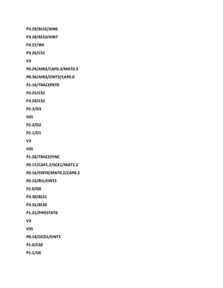
Depending on the hardware configuration
(P1.20, P1.26)
P0.14 is low?](https://image.slidesharecdn.com/armembeddedsystemessentialszlg-230111081204-4bc9ad56/85/ARM-Embedded-System-Essentials-ZLG-docx-373-320.jpg)


![============================
======================
-
147
When RESET is low for the LPC2210/2212/2214, the BOOT1: 0 feet of state control to guide
the way, see Table
5.17. If a pin is not connected, the receiver's internal pull guarantee its high state. Designers
can connect a
To select some weak pull-down resistor (4.7kΩ) or transistor (RESET is low for low drive) to
BOOT1: 0 feet
Boot.
Table 5.17 BOOT1: 0 boot control (LPC2210/2212/2214)
P2.27/D27/BOOT1 P2.26/D26/BOOT0 guide the way MAP1: 0
0 0 CS0 control 8-bit memory 11
16 0 1 CS0 control memory 11
0 CS0 control 32 memory 11
11 internal Flash memory 01
Note the use of the memory-mapped control
Memory-mapped control just necessary from the abnormal processing ARM three data
sources (ie, the exception vector 64 bytes)
Select a use, for LPC2210/2212/2214 the four data sources, as shown in Figure 5.16.
For example, each time to produce a software interrupt request ARM kernel data removed
from 0x00000008 at 32. This
Means when MEMMAP [1:0] = 10 (User RAM mode) from 0x00000008 readings / fetch
0x4000
0008 unit operates. If the MEMMAP [1:0] = 01 (User Flash mode), from 0x00000008 readings
/ take
Means to operate the unit 0x00000008 chip Flash. When MEMMAP [1:0] = 00 (Boot Loader
Mode)
When, from the the 0x00000008 readings / fetch (Boot Block operate 0x7FFFE008 unit of data](https://image.slidesharecdn.com/armembeddedsystemessentialszlg-230111081204-4bc9ad56/85/ARM-Embedded-System-Essentials-ZLG-docx-388-320.jpg)

![====================
==============================
-
149
CCO
FOSC
PLOCK
Bypass
msel <4:0>
M divider
pd
MSEL [4:0]
PSEL [1:0]
fout
cd
1
0
1
cd
/ 2P
PLLC
Direct
PLLE
cclk
FCCO
pd
0
pd
0
1](https://image.slidesharecdn.com/armembeddedsystemessentialszlg-230111081204-4bc9ad56/85/ARM-Embedded-System-Essentials-ZLG-docx-393-320.jpg)
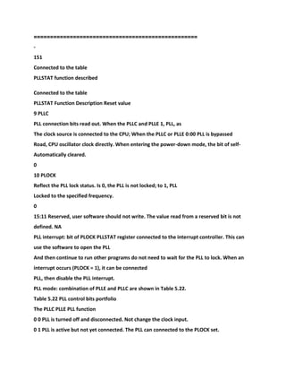
![Write MSEL
Bit value M-1 (see Table 5.25).
� value for P to configure the PSEL bits. By setting the P value FCCO within a defined
frequency limits, FCCO
Can be calculated by the preceding equation. P must be 1, 2, 4 or 8 wherein a. Written to the
PSEL bit values correspond
P-values are shown in Table 5.24.
Table 5.24 PLL divider value
PSEL bit PLLCFG [6:5] P value
00 1
012
104
118
Table 5.25 PLL multiplier value
MSEL bit PLLCFG [4:0] M values
000,001
000,012
000,103
000,114
......
1111031
1111132](https://image.slidesharecdn.com/armembeddedsystemessentialszlg-230111081204-4bc9ad56/85/ARM-Embedded-System-Essentials-ZLG-docx-401-320.jpg)
![==================================================
-
153
PLL set the example.
For example, the system requirements Fosc = 10MHz, cclk = 60MHz.
Based on these requirements can be drawn from the M = cclk / Fosc = 60MHz/10MHz = 6.
Thus, M-1 = 5 write
PLLCFG4: 0.
P values may be P = Fcco / (cclk * 2) derived, Fcco must 156MHz ~ 320MHz within. Assuming
the Fcco take the lowest frequency
The rate of 156MHz, then P = 156MHz / (2 * 60MHz) = 1.3. Fcco take the highest frequency
can be drawn from P = 2.67. Therefore, at the same time
P values satisfy Fcco lowest and highest frequency requirements is only up to 2, as shown in
Table 5.24. So, PLLCFG [6:5] = 01.
5.4.10 VPB divider
1 Description
The VPB Divider decided the relationship between the processor the clock (cclk) and
peripheral devices used by the clock (pclk). VPB
Divider serves two purposes, first by the VPB bus for peripherals the required pclk clock to
peripherals at the right
Speed work. In order to achieve this purpose, the VPB bus can be reduced to 1/2 or 1/4 of the
processor clock rate. Because the VPB
Bus must work properly after power (and when the the VPB divider controller is located VPB
bus leaving on electric
The VPB bus does not work, its timing can not be changed), the VPB bus after reset the
default state in the 1/4 speed run.
The VPB Divider second purpose is to reduce power consumption when the application does
not require any peripherals run at full speed.
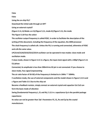
VPB divider and oscillator and the processor clock connection shown in Figure 5.18. VPB](https://image.slidesharecdn.com/armembeddedsystemessentialszlg-230111081204-4bc9ad56/85/ARM-Embedded-System-Essentials-ZLG-docx-402-320.jpg)
![divider is connected to the output of the PLL
PLL remains active (in the idle mode if the PLL is running).
PLL
(Fosc)
VPB divider
(Cclk)
(Pclk)
Crystal or external clock source processor clock
VPB clock
Figure 5.18 VPB divider connected
2. VPBDIV register (the VPBDIV - 0xE01FC100)
The VPB divider registers are described in Table 5.26. VPBDIV [1:0] two bits can be set to
three sub-frequency values as shown in Table
5.27. Effectively XCLKDIV in LPC2210/2212/2214.
Table 5.26 VPBDIV register map
Address Name Description Access
0xE01FC100 VPBDIV control the relationship between the the VPB clock rate of the processor
clock R / W
The Table 5.27 VPBDIV register
VPBDIV Function Description Reset value
1:0 VPBDIV VPB clock rate is as follows:
00: VPB bus clock is 1/4 of the processor clock.
01: VPB bus clock is the same as the processor clock.
10: VPB bus clock is 1/2 of the processor clock.
11: reserved. The value to to write VPBDIV register invalid (to retain the original settings).
0](https://image.slidesharecdn.com/armembeddedsystemessentialszlg-230111081204-4bc9ad56/85/ARM-Embedded-System-Essentials-ZLG-docx-403-320.jpg)
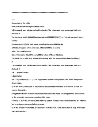
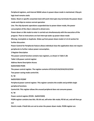
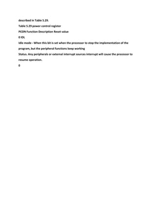
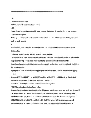
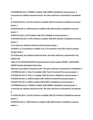
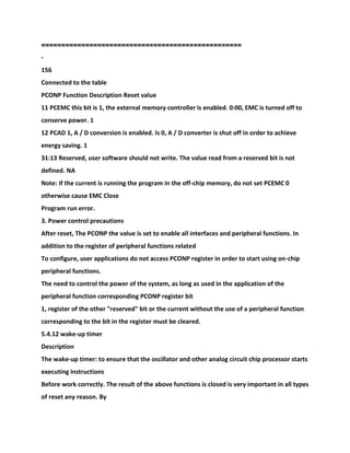
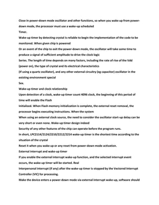
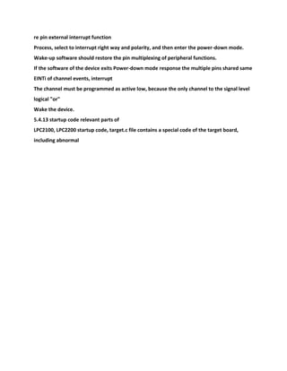
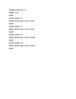
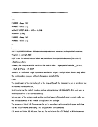

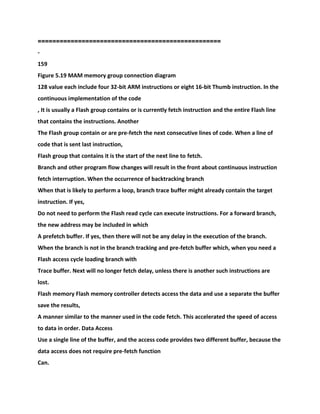
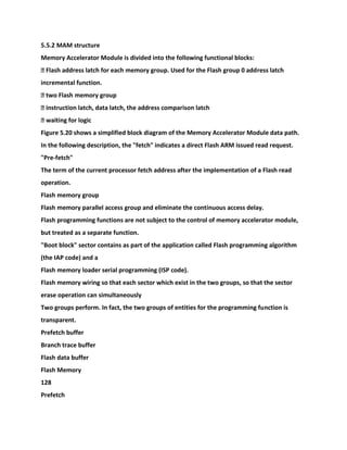
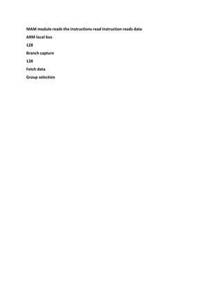


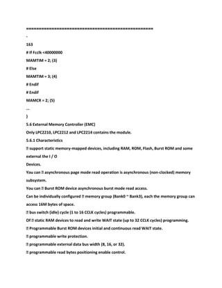
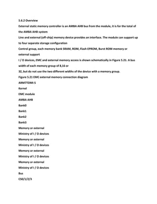
![==================================================
-
164
The LPC2200 series microcontroller pin address output lines A [23:0], which address bits A
[25:24] 4 deposit
The decoding of the reservoir group. The effective area of the four groups of the memory is
located in the initial portion of the external memory, the address, such as shown in Table
5.37.
, Bank 0 can be used to guide the program to run in the pin the BOOT1: 0 state control.
Table 5.37 the address range of the external memory
Bank address range configuration register
0 8000 0000-80FF FFFF BCFG0
1 8100 0000-81FF FFFF BCFG1
2 8200 0000-82FF FFFF BCFG2
3 8300 0000-83FF FFFF BCFG3
Bank0 ~ Bank3 chip select signals CS0 ~ CS3, if the off-chip memory or I / O devices through
CS0
Chip Select CS0 address lines, chip select decoding, this chip memory or I / O devices
belonging Bank0,
Group address 0x80000000 ~ 0x80FFFFFF.
5.6.3 Pin Description
External memory controller pins are described in Table 5.38. These pins P1, P2 and P3 port
GPIO function reuse
To properly first before using the external bus configuration PINSEL2 register (can be set
through hardware pin the BOOT1: 0
Reset the microprocessor automatically initialized PINSEL2; or software initialization PINSEL2,
this only applies to
Chip FLASH boot program running in the system).
Pin Description Table 5.38 External memory controller](https://image.slidesharecdn.com/armembeddedsystemessentialszlg-230111081204-4bc9ad56/85/ARM-Embedded-System-Essentials-ZLG-docx-431-320.jpg)
![Pin Name Type Pin Description
D [31:0] input / output external memory data lines
A [23:0] output External memory address line
The OE output output enable signal, active low
BLS [3:0] output bytes positioning selection signal, low effective
WE write enable signal output, active low
CS [3:0] output chip select signal, active low
5.6.4 Register Description
Register confluence
The external memory controller includes four registers, as shown in Table 5.39.
Table 5.39 External memory controller register
Name Description Access Reset value address
The group 0 BCFG0 memory configuration register read / write 0x2000 FBEF 0xFFE00000
BCFG1 memory group 1 configuration register read / write 0x2000 FBEF 0xFFE00004
BCFG2 memory group configuration register read / write 0x1000 FBEF 0xFFE00008
BCFG3 memory group configuration register read / write 0x0000 FBEF 0xFFE0000C
Note: Bank 0 can be used to guide the program to run, to set BCFG0 reset value pin BOOT1: 0,
are shown in Table 5.41.
Each register for the corresponding memory bank configured with the following options:](https://image.slidesharecdn.com/armembeddedsystemessentialszlg-230111081204-4bc9ad56/85/ARM-Embedded-System-Essentials-ZLG-docx-432-320.jpg)
![==================================================
-
166
Connected to the table
BCFG0-3 Name Function Reset value
26 WP, the bit is set to 1, indicating that the write-protected memory group. 0
27 BM bit is set to 1, indicating that the memory group is Burst ROM. 0
This field controls the width of the data bus of the memory group in 29:28 MW: 00 = 8, 01 =
16, 10 = 32
Bit 11 = reserved.
See Table
5.41
31:30 AT domain usually write 0000
Bank 0 can be used to guide the program to run, so BCFG0 [29:28] Reset Value of pin BOOT1:
0 set
The set, shown in Table 5.41. Description: BOOT1: 0 = 11, from the on-chip FLASH boot
program running.
Table 5.41 reset default memory width
Bank reset the time the BOOT1: 0 state BCFG [29:28] reset value memory width
0 LL 00 8-bit
0 LH 01 16-bit
0 HL 10 32
0 HH 10 32
1 XX 10 32
2 XX 01 16-bit
3 XX 00 8-bit
5.6.5 External Memory Interface
The external memory interface depends on the width of the memory group (32, 16 or 8-bit
Select from the the BCFG register the MW](https://image.slidesharecdn.com/armembeddedsystemessentialszlg-230111081204-4bc9ad56/85/ARM-Embedded-System-Essentials-ZLG-docx-436-320.jpg)
![==================================================
-
167
A [a_b: 2]
BLS [1]
D [15:8]
CE
OE
WE
IO [7:0]
A [a_m: 0]
BLS [0]
D [7:0]
CE
OE
WE
IO [7:0]
A [a_m: 0]
OE
CS
BLS [3]
D [31:24]
CE
OE
WE
IO [7:0]
A [a_m: 0]
BLS [2]
D [23:16]](https://image.slidesharecdn.com/armembeddedsystemessentialszlg-230111081204-4bc9ad56/85/ARM-Embedded-System-Essentials-ZLG-docx-438-320.jpg)
![CE
OE
WE
IO [7:0]
A [a_m: 0]
a) 32-bit wide memory group connected 8-bit memory chips
b) 32-bit wide memory group connected to a 16-bit memory chips
OE
CS
WE
CE
OE
WE
B3
B2
B1
B0
IO [31:0]
A [a_m: 0]
D [31:0]
BLS [2]
A [a_b: 0]
BLS [3]
BLS [0]
BLS [1]
c) a 32-bit wide memory group connected to a 32-bit memory chips
OE
CS
WE](https://image.slidesharecdn.com/armembeddedsystemessentialszlg-230111081204-4bc9ad56/85/ARM-Embedded-System-Essentials-ZLG-docx-439-320.jpg)
![CE
OE
WE
UB
LB
IO [15:0]
A [a_m: 0]
D [31:16]
BLS [2]
CE
OE
WE
UB
LB
IO [15:0]
A [a_m: 0]
D [15:0]
BLS [0]
A [a_b: 2]
BLS [3] BLS [1]
Figure 5.22 32-bit memory group external memory interface
OE
CS
BLS [1]
D [15:8]
CE
OE
WE
IO [7:0]](https://image.slidesharecdn.com/armembeddedsystemessentialszlg-230111081204-4bc9ad56/85/ARM-Embedded-System-Essentials-ZLG-docx-440-320.jpg)
![A [a_m: 0]
BLS [0]
D [7:0]
CE
OE
WE
IO [7:0]
A [a_m: 0]
A [a_b: 1]
OE
CS
WE
CE
OE
WE
UB
LB
IO [15:0]
A [a_m: 0]
D [15:0]
BLS [0]
A [a_b: 1]
BLS [1]
a) 16-bit wide memory group connected 8-bit memory chip A) 16-bit wide memory group
connected to 16-bit memory chips
Figure 5.23 16-bit memory group external memory interface
OE
CS
BLS [0]](https://image.slidesharecdn.com/armembeddedsystemessentialszlg-230111081204-4bc9ad56/85/ARM-Embedded-System-Essentials-ZLG-docx-441-320.jpg)
![D [7:0]
CE
OE
WE
IO [7:0]
A [a_m: 0]
A [a_b: 0]
Figure 5.24 8 memory group external memory interface](https://image.slidesharecdn.com/armembeddedsystemessentialszlg-230111081204-4bc9ad56/85/ARM-Embedded-System-Essentials-ZLG-docx-442-320.jpg)
![t - t + 5ns
tWRITE <= tCYC * (1 + WST2)-5ns
5.6.8 startup code relevant parts of
LPC2210/2212/2214 is the bus open type chip having a memory group of the four Bank, the
bus width can be
Is set to 8, 16 or 32. LPC2200 startup code in the packet bus initialization settings, such as
program listings 5.11
Shown (in startup.s files).
Program list 5.11 bus configuration initialization
ResetInit
LDR R0, = PINSEL2 (1)
IF: DEF: EN_CRP
LDR R1, = 0x0f814910 (2)
ELSE
LDR R1, = 0x0f814914 (3)
ENDIF
STR R1, [R0] (4)
LDR R0, = BCFG0 (5)
LDR R1, = 0x1000ffef (6)
STR R1, [R0] (7)
LDR R0, = BCFG1 (8)
LDR R1, = 0x1000ffef (9)
STR R1, [R0] (10)
; LDR R0, = BCFG2 (11)
; LDR R1, = 0x2000ffef (12)
; STR R1, [R0] (13)
; LDR R0, = BCFG3 (14)
; LDR R1, = 0x2000ffef (15)
; STR R1, [R0] (16)](https://image.slidesharecdn.com/armembeddedsystemessentialszlg-230111081204-4bc9ad56/85/ARM-Embedded-System-Essentials-ZLG-docx-447-320.jpg)
![1:0 P0.0 GPIO P0.0 TxD (UART0) PWM1 reserved 00
3:2 P0.1 GPIO P0.1 RxD (UART0) PWM3 EINT0 00
5:4 P0.2 GPIO P0.2 SCL (I2C) Capture 0.0 (TIMER0) retained 00
And matching 0.0 (TIMER0) EINT1 00 in 7:6 P0.3 GPIO P0.3 SDA (I2C)
9:8 P0.4 GPIO P0.4 SCK (SPI0) capture 0.1 (TIMER0) retained 00
11:10 P0.5 GPIO P0.5 MISO (SPI0) matching 0.1 (TIMER0) retained 00
13:12 P0.6 GPIO P0.6 MOSI (SPI0) Capture 0.2 (TIMER0) retained 00
15:14 P0.7 GPIO P0.7 SSEL (SPI0) PWM2 EINT2 00
17:16 P0.8 GPIO P0.8 TxD UART1 PWM4 reserved 00
19:18 P0.9 GPIO P0.9 RxD (UART1) PWM6 EINT3 00
21:20 P0.10 GPIO P0.10 RTS (UART1) Capture 1.0 (TIMER1) retained 00
23:22 P0.11 GPIO P0.11 CTS (UART1) Capture 1.1 (TIMER1) retained 00
Match 1.0 (TIMER1) retained 00 25:24 P0.12 GPIO P0.12 DSR (UART1)
Match 1.1 (TIMER1) retained 00 27:26 P0.13 GPIO P0.13 DTR (UART1)
29:28 P0.14 GPIO P0.14 CD (UART1) EINT1 reserved 00
31:30 P0.15 GPIO P0.15 RI (UART1) EINT2 reserved 00
Description: Table 5.44 "PINSEL0" the column indicates PINSEL0 register
control bit, "Pin Name" column shows the control bits of the control
The pin, "00/01/10 / / 11" column shows the control pin functions in these
settings. For example, P0.0 pin control bit PINSEL0 [1:0]](https://image.slidesharecdn.com/armembeddedsystemessentialszlg-230111081204-4bc9ad56/85/ARM-Embedded-System-Essentials-ZLG-docx-450-320.jpg)
![==================================================
-
171
When PINSEL0 [1:0] = 00 pin GPIO function (P0.0), when PINSEL0 [1:0] =
01 when the pin for UART0 TxD function foot
When PINSEL0 [1:0] = 10 pins for the PWM1 pin.
Pin Function Select in register (PINSEL1 - 0xE002C004)
PINSEL1 register in accordance with the settings in the table 5.45 to control
the function of the pin. IODIR direction control register
The bit is only effective in pin select GPIO functions only. For other functions,
direction is controlled automatically.
Table 5.45 Pin Select Register
PINSEL1 pin name 00011011 reset value
1:0 P0.16 GPIO P0.16 EINT0 match
0.2 (TIMER0)
Retain 00
3:2 P0.17 GPIO P0.17 capture 1.2 (TIMER1) SCK (SPI1) matching 1.2
(TIMER1) 00
5:4 P0.18 GPIO P0.18 capture 1.3 (TIMER1) MISO (SPI1) matching 1.3
(TIMER1) 00
7:6 P0.19 GPIO P0.19 match 1.2 (TIMER1) MOSI (SPI1) matching 1.3
(TIMER1) 00
9:8 P0.20 GPIO P0.20 match 1,3 (TIMER1) SSEL (SPI1) EINT3 00
11:10 P0.21 GPIO P0.21 PWM5 reserved capture 1.3 (TIMER1) 00
13:12 P0.22 GPIO P0.22 reserved capture
0.0 (TIMER0)
Match 0.0 (TIMER0) 00](https://image.slidesharecdn.com/armembeddedsystemessentialszlg-230111081204-4bc9ad56/85/ARM-Embedded-System-Essentials-ZLG-docx-451-320.jpg)
![15:14 P0.23 GPIO P0.23 reserved reserved reserved 00
17:16 P0.24 GPIO P0.24 reserved reserved reserved 00
19:18 P0.25 GPIO P0.25 reserved reserved reserved 00
21:20 P0.26 reserved 00
23:22 P0.27 GPIO P0.27 AIN0 (A / D converter) capture
0.1 (TIMER0)
Match 0.1 (TIMER0) 01
25:24 P0.28 GPIO P0.28 AIN1 (A / D converter) capture
0.2 (TIMER0)
Match 0.2 (TIMER0) 01
27:26 P0.29 GPIO P0.29 AIN2 (A / D converter) capture
0.3 (TIMER0)
Match 0.3 (TIMER0) 01
29:28 P0.30 GPIO P0.30 AIN3, respectively (A / D converter) EINT3 capture
the 0.0 (TIMER0) 01
31:30 P0.31 reserved 00
PINSEL register control table 5.46 of the pins. Every two register bit
corresponds to a specific device cited
Feet. PINSEL1 [23:22] [25:24], [27:26], [29:28] reset value of 01.
Table 5.46 Pin function select register bit
The value function reset PINSEL0 and PINSLE1 value
00 preferred (default) function, usually as a GPIO port
01 optional features
The second optional features 10
11 Reserved
00
Pin function select register 2 (PINSEL2 - 0xE002C014)](https://image.slidesharecdn.com/armembeddedsystemessentialszlg-230111081204-4bc9ad56/85/ARM-Embedded-System-Essentials-ZLG-docx-452-320.jpg)

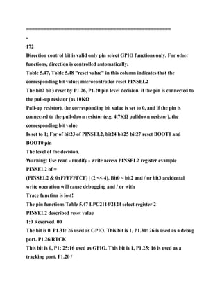
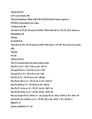

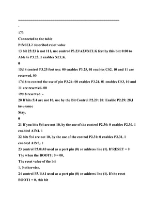
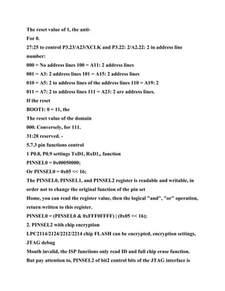
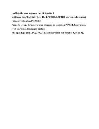
![==================================================
-
174
For not using the bus pins (such as the 16-bit bus width, D16 ~ D31 did not
use), can be used as GPIO
To use. LPC2200 startup code package P1, P2 and P3 port initialization
settings, as shown in program list 5.12 (in
file) of startup.s.
5.12 bus pin set of program listings
ResetInit
LDR R0, = PINSEL2 (1)
IF: DEF: EN_CRP
LDR R1, = 0x0f814910 (2)
ELSE
LDR R1, = 0x0f814914 (3)
ENDIF
STR R1, [R0] (4)
...
Program list 5.12 when predefined EN_CRP macro will compile the program
list 5.12 (2), PINSEL2
Is set to 0x0f814910, disable the JTAG debugging; if not the definition
EN_CRP macro will compile the program list 5.12
(3), PINSEL2 set to 0x0f814914, debugging using the JTAG port.
Startup.s file, the user not find defined EN_CRP macro code does not need to
go directly to define
The EN_CRP macro, because the LPC2200 project template to use, as long as
selected RelInChip target, the compiler will be predefined](https://image.slidesharecdn.com/armembeddedsystemessentialszlg-230111081204-4bc9ad56/85/ARM-Embedded-System-Essentials-ZLG-docx-460-320.jpg)
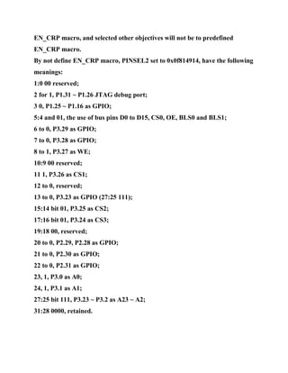
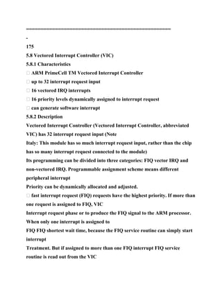
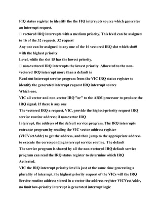
![The system. Other information, please refer to the the ARM PrimeCell TM
vector Vectored Interrupt Controller Interrupt Controller (PL190)
Related documentation.
Use the VIC IRQ interrupt the process shown in Figure 5.27, the user
program must first initialize the the VIC so can related
Off, then the normal operation of the user program (see Figure 5.27 in ①);
IRQ interrupt is generated, VIC interrupt will
Source set VICVectAddr register for the corresponding interrupt service
routine address (see Figure 5.27 in ②), switch the processor work
Mode to IRQ mode, and jump to the IRQ interrupt entrance 0x00000018
(Figure 5.27 ③); exception vector
0x00000018 at the use of a "LDR PC, [PC, #-0xff0] instruction, instruction
will read VICVectAddr
The value of the register is then placed in the PC program pointer to jump to
the corresponding interrupt service routine (Figure 5.27 in ④); interrupt
service
Service in executing the corresponding interrupt handling, clear the interrupt
flag ⑤ in Figure 5.27; interrupt service is completed, you can return
Original breakpoint (Figure 5.27 in ⑥) Note that the return to the switch
processor mode.](https://image.slidesharecdn.com/armembeddedsystemessentialszlg-230111081204-4bc9ad56/85/ARM-Embedded-System-Essentials-ZLG-docx-464-320.jpg)
![==================================================
-
176
Figure 5.27 using the VIC IRQ interrupt processing
5.8.3 The structure
Vector interrupt controller block diagram shown in Figure 5.28.
RawInterrupt
[31:0]
IntSelect
[31:0]
IntEnable
[31:0]
SoftInt
[31:0]
VICINT
SOURCE
[31:0]
FIQStatus
[31:0]
IRQStatus
[31:0]
VectorAddr
[31:0]
VectIRQ0
VectAddr0 [31:0]
VectorCntl [5:0]
Source Enable](https://image.slidesharecdn.com/armembeddedsystemessentialszlg-230111081204-4bc9ad56/85/ARM-Embedded-System-Essentials-ZLG-docx-465-320.jpg)
![VectIRQ1
VectAddr1 [31:0]
VectIRQ15
VectAddr15 [31:0]
Default
VectorAddr
[31:0]
VectorAddr
[31:0]
nVICIRQIN VICVECTADDRIN [31:0]
IRQ nVICIRQ
VICVECT
ADDROUT
[31:0]
nVICFIQ
FIQStatus
[31:0]
nVICFIQIN
IRQStatus NonVectIRQ
[31:0]
IRQ
SoftIntClear
[31:0]
IntEnableClear
[31:0]
Interrupt request, shielding, and selection
Non-vectored FIQ interrupt logic](https://image.slidesharecdn.com/armembeddedsystemessentialszlg-230111081204-4bc9ad56/85/ARM-Embedded-System-Essentials-ZLG-docx-466-320.jpg)
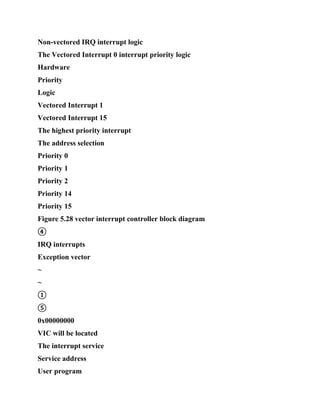
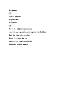
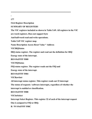
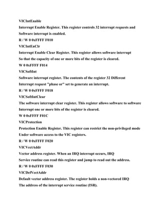

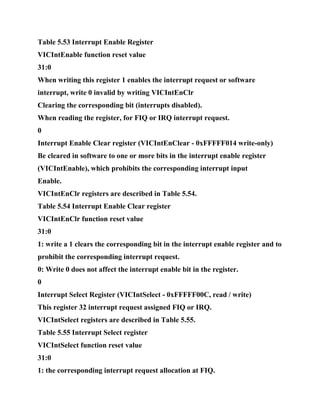

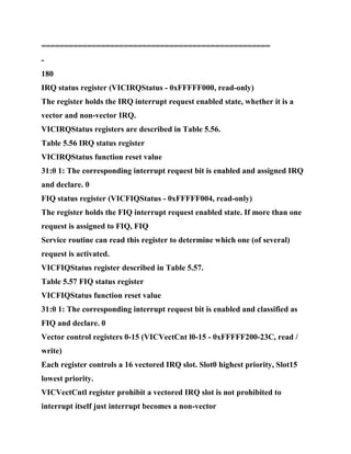
![Form. VICVectCntl [4:0] for this interrupt source assigned IRQ slot number,
the source of the interrupt number shown in Table 5.63.
VICVectCntl0-15 registers are described in Table 5.58.
Table 5.58 vector control register 0-15
VICVectCntl0-15 function reset value
5
1: Enable vectored IRQ assigned interrupt request or software interrupt
enable as IRQ and sound
Ming, can produce a unique ISR address the (read VICVectAddr register).
0
4:0
The number assigned to this vectored IRQ slot interrupt request or software
interrupt.
Do not will the same interrupt number assigned to more than one enabled
vectored IRQ slots. But if this
Do so, when the interrupt request or software interrupt enable, and was
assigned as IRQ, and asserted, will use the most
Low-numbered slot.
0
Vector Address Register 0-15 (VICVectAddr0-15 - 0xFFFFF100-13C, read /
write)
These registers hold the 16 vectored IRQ slot is the address of the interrupt
service routine (ISR).
VICVectAddr0-15 registers are described in Table 5.59.
Table 5.59 Vector Address Register 0-15
VICVectAddr0-15 function reset value
31:0](https://image.slidesharecdn.com/armembeddedsystemessentialszlg-230111081204-4bc9ad56/85/ARM-Embedded-System-Essentials-ZLG-docx-479-320.jpg)

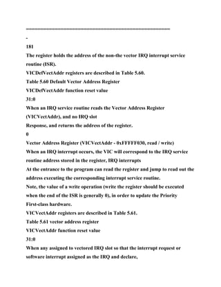

![VICIntEnable 0x000006C0 (SPI0, I2C, UART1 and UART0 interrupt enable
=> bit10, bit9,
bit 7 and bit6 = 1)
VICDefVectAddr = 0x ... (save the non-vectored IRQ service program
address, ie UART1 and I2C
Service routine start address)
VICVectAddr0 = 0x ... (save UART0 IRQ service routine start address)
VICVectAddr1 = 0x ... (save SPI0 IRQ service routine start address)
VICVectCntl0 = 0x00000026 source (the VIC channel number to 6 (UART0)
interrupt enable priority 0
(Highest priority))
VICVectCntl1 = 0x0000002A (the VIC channel number 10 (SPI0) interrupt
source for Priority 1)
Jump to address any IRQ requests (SPI0, I2C, UART0 or UART1)
microcontroller
The 0x00000018 code execution. Vector and non-vector IRQ address 0x18 into
the following instruction:
LDR pc, [pc, #-0xFF0]
The instruction address VICVectAddr register into the PC.
The once produced the the UART0 requests, VICVectAddr and
VICVectAddr0 same. If an SPI request
VICVectAddr equal VICVectAddr1. UART0 and SPI IRQ request but
UART1 and](https://image.slidesharecdn.com/armembeddedsystemessentialszlg-230111081204-4bc9ad56/85/ARM-Embedded-System-Essentials-ZLG-docx-489-320.jpg)

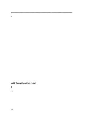
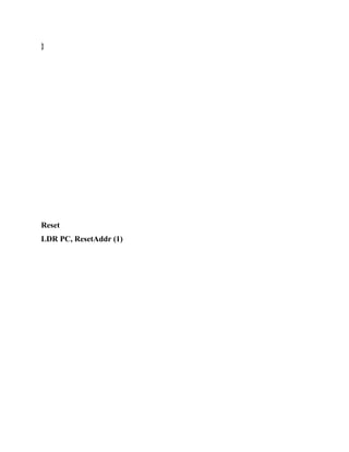
![==================================================
-
LDR PC, UndefinedAddr (2)
LDR PC, SWI_Addr (3)
LDR PC, PrefetchAddr (4)
LDR PC, DataAbortAddr (5)
DCD 0xb9205f80 (6)
LDR PC, [PC, #-0xff0] (7)
LDR PC, FIQ_Addr (8)
ResetAddr DCD ResetInit (9)
UndefinedAddr DCD Undefined (10)
SWI_Addr DCD SoftwareInterrupt (11)
PrefetchAddr DCD PrefetchAbort (12)
DataAbortAddr DCD DataAbort (13)
Nouse DCD 0 (14)
IRQ_Addr DCD 0 (15)
FIQ_Addr DCD FIQ_Handler (16)
...](https://image.slidesharecdn.com/armembeddedsystemessentialszlg-230111081204-4bc9ad56/85/ARM-Embedded-System-Essentials-ZLG-docx-494-320.jpg)


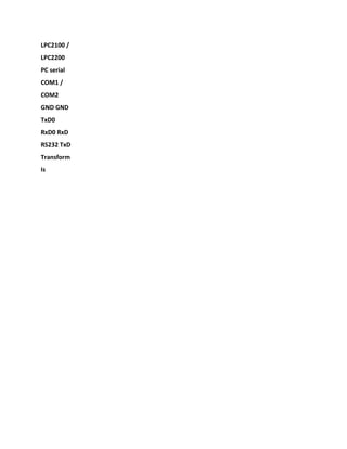
![==================================================
-
191
Interrupt interface to contain register U0IER and The U0IIR. Interrupt interface receives
several issued by U0Tx and U0Rx, single
The clock width of the enable signal.
NTXRDY
TxD0
NBAUDOUT
RCLK
RxD0
NRXRDY
U0THR U0TSR
U0Tx
U0BRG
U0DLL
U0DLM
U0RSR
U0Rx
U0RBR
U0FCR
U0LSR
UL0CLCRR
VPB DDIS
U0SCR
U0IER
U0IIR
pclk
PA [2:0]](https://image.slidesharecdn.com/armembeddedsystemessentialszlg-230111081204-4bc9ad56/85/ARM-Embedded-System-Essentials-ZLG-docx-506-320.jpg)
![PSEL
PSTB
PWRITE
PD [7:0]
AR
MR
U0INTR
Interface
Interrupt
The block diagram of Figure 5.32 UART0
5.10.5 Register Description
SUMMARY OF REGISTERS
The UART0 contain 10 8-bit registers, as shown in Table 5.72. Divisor Latch Access Bit (DLAB)
located U0LCR
bit7, it enabled the divisor latch access.
To Table 5.72 UART0 register mapping
Name Description Access Reset Value BIT7 BIT6 BIT5 BIT4 BIT3 BIT2 BIT1 BIT0 * Address
U0RBR receiving buffer MSB read the data LSB RO undefined
0xE000C000
DLAB = 0
U0THR send keep MSB write data LSB WO NA
0xE000C000
DLAB = 0
U0IER interrupt enable 00000
Enable Rx
Line status interrupt
Enable the THRE
Interrupt
Enable Rx data](https://image.slidesharecdn.com/armembeddedsystemessentialszlg-230111081204-4bc9ad56/85/ARM-Embedded-System-Essentials-ZLG-docx-507-320.jpg)

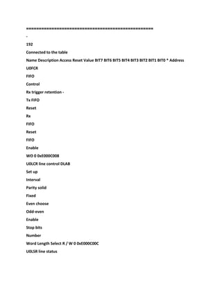
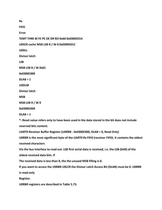
![1: Enable the Rx line status interrupt
U0IER2 enable UART0 Rx line status interrupts. The state of the interrupt from U0LSR [4:1]
Read out.
0
7:3 Reserved, user software should not write. The value read from a reserved bit is not
defined. NA
UART0 Interrupt Identification Register (U0IIR - 0xE000C008, read-only)
U0IIR status code is used to indicate a pending interrupt source interrupt priority. In the
access U0IIR,
The interrupt is frozen. If visit to U0IIR, when the interrupt, the interrupt is recorded the next
U0IIR access readable out.
U0IIR registers are described in Table 5.78.](https://image.slidesharecdn.com/armembeddedsystemessentialszlg-230111081204-4bc9ad56/85/ARM-Embedded-System-Essentials-ZLG-docx-514-320.jpg)
![==================================================
-
194
Table 5.78 UART0 Interrupt Identification Register
U0IIR Function Description Reset value
0 interrupt pending
0: At least one interrupt is pending
1: No pending interrupts
U0IIR0 lower effective. Pending interrupt can be determined by U0IER3: 1.
1
3:1 Interrupt Identification
011:1. Receive Line Status (RLS)
010:2 a. Receive Data Available (RDA)
110:2 b. Character out Indicator (CTI)
001:3. THRE interrupt
U0IER the bit3 instructions corresponding to the UART0 Rx FIFO interrupt. Not listed above
The other combinations U0IER [3:1] are reserved (000, 100, 101, 111)
0
5:4 Reserved, user software should not write. The value read from a reserved bit is not
defined. NA
7:6 FIFO Can these bits is equivalent to U0FCR bit0 0
The UART0 interrupt source interrupt enable relationship as shown in Figure 5.33.
Figure 5.33 UART0 interrupt sources and interrupt enable diagram
Interrupt the processing shown in Table 5.79. Given U0IIR [3:0] state, the interrupt handler
can determine the interrupt source as well as
How to clear an active interrupt. Before exiting the interrupt service routine, must to read
U0IIR to clear the interrupt.
Table 5.79 UART0 interrupt handling
U0IIR [3:0] priority interrupt type interrupt source interrupt reset](https://image.slidesharecdn.com/armembeddedsystemessentialszlg-230111081204-4bc9ad56/85/ARM-Embedded-System-Essentials-ZLG-docx-515-320.jpg)
![0001 - None -
The 0110 highest Rx line status / error OE, PE, FE or BI U0LSR read operation
0100 second Rx data available
Rx data available or FIFO mode (U0FCR0 = 1) reaches the trigger
Point
U0RBR read or
UART0 FIFO
Trigger value
RLS (U0IIR [3:1] = 011)
U0IER the bit2
RDA (U0IIR [3:1] = 010)
U0IER the bit0
CTI (U0IIR [3:1] = 110)
THRE interrupt
(U0IIR [3:1] = 001)
U0IER the bit1
VIC
Interrupt controller
Controller
ARM7
TDMIS
Kernel](https://image.slidesharecdn.com/armembeddedsystemessentialszlg-230111081204-4bc9ad56/85/ARM-Embedded-System-Essentials-ZLG-docx-516-320.jpg)
![==================================================
-
195
Connected to the table
U0IIR [3:0] priority interrupt type interrupt source interrupt reset
1100 second character timeout indication
Rx FIFO contains at least one character, and in a period of time without words
Character input or removed from, the length of time depends on the characters in the FIFO
Number as well as trigger values in the 3.5 to 4.5 characters time.
The actual time is:
[(Word length) × 7-2 × 8 + [(trigger value - the number of characters) × 8 + 1] PCLK
U0RBR read operation
0010 Third THRE
The THRE U0IIR read or
THR write
Note: "0000", "0011", "0101", "0111", "1000", "1001", "1010", "1011", "1101", "1110",
"1111" is reserved.
� UART0 RLS interrupt (U0IIR [3:1] = 011) is the highest priority interrupt. As long as UART0 Rx
input
Produces 4 error conditions (overflow error (OE), parity error (PE), framing error (FE) and
interval interrupt
(Bi)) in any one of the interrupt flag is set. This interrupt will UART0 Rx error conditions
View An U0LSR [4:1] get. Interrupt when read U0LSR clear.
� UART0 RDA interrupt (U0IIR [3:1] = 010) and CTI interrupt (U0IIR [3:1] = 110) shares the
second excellent
First grade. , RDA is activated when the UART0 Rx FIFO reaches the U0FCR7: 6 defined trigger
point. When
UART0 Rx FIFO depth below the trigger point, RDA reset. When the RDA interrupt goes active,
the CPU](https://image.slidesharecdn.com/armembeddedsystemessentialszlg-230111081204-4bc9ad56/85/ARM-Embedded-System-Essentials-ZLG-docx-517-320.jpg)
![Reading out a block of data defined by the trigger.
� UART0 CTI interrupt (U0IIR [3:1] = 110) as the second priority interrupt. When the UART0 Rx
FIFO contains
UART0 Rx FIFO action did not occur within the time at least one of the characters and
receives 3.5 to 4.5 characters.
Generate the interrupt. UART0 Rx FIFO any action (read or write UART0 RBR) will clear the
interrupt.
When the information received is not the trigger value multiples, CTI interrupt is intended to
flush the UART0 the RBR. For example, if
If a peripheral wants to send a 105-character information, and trigger value of 10 characters,
then the top 100
The characters will receive 10 RDA interrupt CPU, while the remaining five characters so that
the CPU receives 1-5
CTI interrupts (depending on the service routine).
� UART0 THRE interrupt (U0IIR [3:1] = 001) for the third-priority interrupt. When the UART0
THR FIFO
Empty and meet specific initialization conditions activate the interrupt. These initialization
conditions will enable UART0 THR
FIFO is populated with data, to avoid many THRE interrupt is generated when the system
starts. Initialization conditions THRE = 1
When one character delay minus the stop bit, and in the last time the THRE = 1 event not
U0THR
In the presence of at least two characters. In without decoding and services THRE interrupt,
the delay for the CPU provides
Time of the the data write U0THR the. UART0 THR FIFO has two or more characters, and
when
, THRE interrupt is set immediately the former U0THR is empty. When an U0THR to write the
operation or U0IIR read operation
(U0IIR3: 1 = 001) and the THRE is the highest priority interrupt, THRE interrupt reset.](https://image.slidesharecdn.com/armembeddedsystemessentialszlg-230111081204-4bc9ad56/85/ARM-Embedded-System-Essentials-ZLG-docx-518-320.jpg)
![UART0 FIFO Control Register (U0FCR - 0xE000C008)
U0FCR control the operation of the UART0 Rx and Tx FIFO.
U0FCR registers are described in Table 5.80.
Table 5.80 UART0 FIFO Control Register
U0FCR Function Description Reset value
0 FIFO enabled
1:00 to enable access UART0 Rx and Tx FIFO U0FCR [7:1]. This bit
Must be set in order to achieve the correct operation of the UART0. Any variation of the bit
will make UART0
Clearing the FIFO.
0](https://image.slidesharecdn.com/armembeddedsystemessentialszlg-230111081204-4bc9ad56/85/ARM-Embedded-System-Essentials-ZLG-docx-519-320.jpg)
![U0LCR Function Description Reset value
1:0 word length select
00:5 bit character length
01:6 bit character length
10:7 bit character length
11:8 bit character length
0
2 stop bits selection
0:1 a stop bit
1:2 stop bit (if U0LCR [1:0] = 00, compared with 1.5)
0
3 Parity Enable
0: Disable parity generation and checking
1: Enable parity generation and check
0
5:4 parity selection
00: Odd
01: Even
10: Forced to 1
11: Forced to 0
0
6 interval control
0: Disable the interval for sending
1: Enable interval send
When U0LCR the bit6 1, Output pin UART0 TxD is forced to logic 0.
0
7 Divisor Latch Access Bit
0: Disable access to divisor latch register
1: Enable access to divisor latch register](https://image.slidesharecdn.com/armembeddedsystemessentialszlg-230111081204-4bc9ad56/85/ARM-Embedded-System-Essentials-ZLG-docx-521-320.jpg)
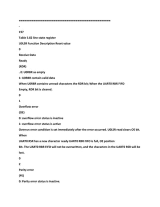
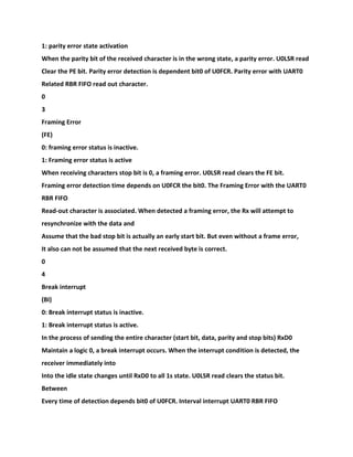
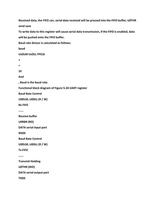

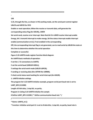
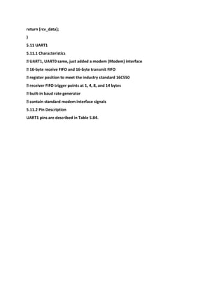
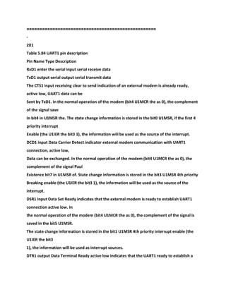
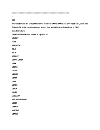
![U1IER
U1IIR
pclk
PA [2:0]
PSEL
PSTB
PWRITE
PD [7:0]
AR
MR
U1INTR
RTS
DTR
CTS
DSR
DCD
RI
Interrupt
Figure 5.37 UART1 block diagram
VPB interface provides communication between the CPU and the UART1 connection.
The the UART1 receiver module U1Rx monitoring the serial input line RxD1 of the effective
input. UART1 Rx Shift Register
(U1RSR) by RxD1 accept valid character. When U1RSR received a valid character, pass the
character
Sent to the UART1 Rx buffer register FIFO wait for CPU access by VPB interface.
Data cache and data the UART1 Transmitter module U1Tx accept CPU written to UART1 Tx
holding register
FIFO (U1THR) in. The UART1 Tx shift register (U1TSR) reads the data and the data in the
U1THR by string](https://image.slidesharecdn.com/armembeddedsystemessentialszlg-230111081204-4bc9ad56/85/ARM-Embedded-System-Essentials-ZLG-docx-537-320.jpg)
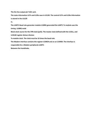
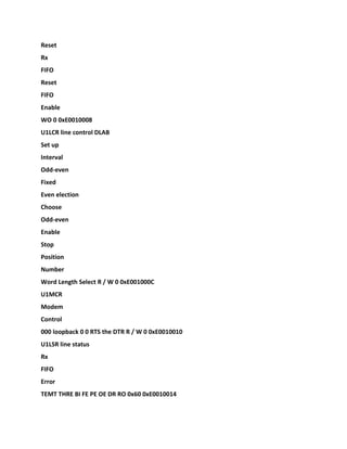
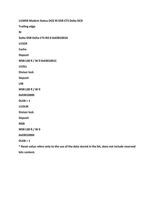
![Enable
0: Disable the THRE interrupt
1: Enable the THRE interrupt
U1IER1 can UART1 THRE interrupt. The status of this interrupt can be read out from U1LSR5.
0
2
Rx line status
Interrupt Enable
0: prohibit Rx line status interrupt
1: Enable the Rx line status interrupt
U1IER2 energy UART1 Rx line status interrupts. The interrupt status can be read from U1LSR
[4:1]
A.
0
3
Modem-like
State interrupt enable
0: prohibit Modem interrupt
1: Enable interrupt Modem
U1IER3 to enable modem interrupted. Interrupt status can be read from U1MSR [3:0].
0
7:4 Reserved, user software should not write. The value read from a reserved bit is not
defined. NA
UART1 Interrupt Identification Register (U1IIR - 0xE0010008, read-only)
U1IIR status code is used to indicate a pending interrupt sources and priority, see Table 5.91.
Visit U1IIR
Process, the interrupt is frozen. If visit to U1IIR, when interrupt, the interrupt is recorded, the
next U1IIR access
Read out.](https://image.slidesharecdn.com/armembeddedsystemessentialszlg-230111081204-4bc9ad56/85/ARM-Embedded-System-Essentials-ZLG-docx-546-320.jpg)
![==================================================
-
206
Connected to the table
U1IIR Function Description Reset value
3:1 Interrupt Identification
011:1. Receive Line Status (RLS)
010:2 a. Receive Data Available (RDA)
110:2 b. Character out Indicator (CTI)
001:3. THRE interrupt
000:4. Modem interrupt
U1IER the bit3 instructions corresponding to the UART1 Rx FIFO interrupt. U1IER3 instructions
corresponding to the
UART1 Rx FIFO interrupt. Above is not listed U0IER [3:1] of the other combinations are
reserved.
Value (100, 101, 111)
0
5:4 Reserved, user software should not write. The value read from a reserved bit is not
defined. NA
7:6 FIFO enable bit is equivalent to U1FCR0 0
UART1 interrupt source interrupt enable relationship is shown in Figure 5.38.
Figure 5.38 UART1 interrupt sources and interrupt enable diagram
Interrupt the processing shown in Table 5.92. Given U1IIR [3:0] state, the interrupt handler
can determine the interrupt source as well as
How to clear an active interrupt. Before exiting the interrupt service routine, must to read
U1IIR to clear the interrupt.
Table 5.92 UART1 interrupt handling
U1IIR [3:0] priority interrupt type interrupt source interrupt reset
0001 - None -](https://image.slidesharecdn.com/armembeddedsystemessentialszlg-230111081204-4bc9ad56/85/ARM-Embedded-System-Essentials-ZLG-docx-548-320.jpg)
![The 0110 highest Rx line status / error OE, PE, FE or BI U1LSR read operation
0100 second Rx data available
Rx data available or FIFO mode (FCR0 = 1) to
Up to the trigger point
U1RBR read or FIFO
Trigger value
RLS (U1IIR [3:1] = 011)
U1IER the bit2
RDA (U1IIR [3:1] = 010)
U1IER the bit0
CTI (U1IIR [3:1] = 110)
THRE interrupt
(U1IIR [3:1] = 001)
U1IER the bit1
VIC
Interrupt controller
Controller
ARM7
TDMIS
Kernel
Modem interrupt
(U1IIR [3:1] = 000)
U1IER the bit3](https://image.slidesharecdn.com/armembeddedsystemessentialszlg-230111081204-4bc9ad56/85/ARM-Embedded-System-Essentials-ZLG-docx-549-320.jpg)
![=========
=========================================
-
207
Connected to the table
U1IIR [3:0] priority interrupt type interrupt source interrupt reset
1100 second character timeout indication
Rx FIFO contains at least one character, and in a period of time without words
Character input or removed from, the length of time depends on the characters in the FIFO
Number characters (from 3.5 to 4.5 hours) trigger value. Real
's Time for the occasion:
[(Word length) × 7-2 × 8 + [(trigger value - the number of characters) × 8 + 1] PCLK
U1RBR read operation
0010 Third THRE THRE
The U1IIR read (if in
Source of the interrupt) or THR write
The 0000 fourth Modem status CTS, DSR, RI, DCD MSR read operation
Note: "0011", "0101", "0111", "1000", "1001", "1010", "1011", "1101", "1110", "1111" is
reserved.
� UART1 RLS interrupt (U1IIR [3:1] = 011) is the highest priority interrupt.
When](https://image.slidesharecdn.com/armembeddedsystemessentialszlg-230111081204-4bc9ad56/85/ARM-Embedded-System-Essentials-ZLG-docx-550-320.jpg)


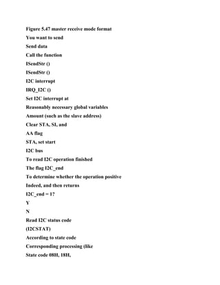

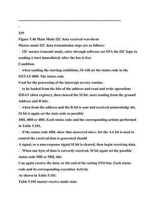
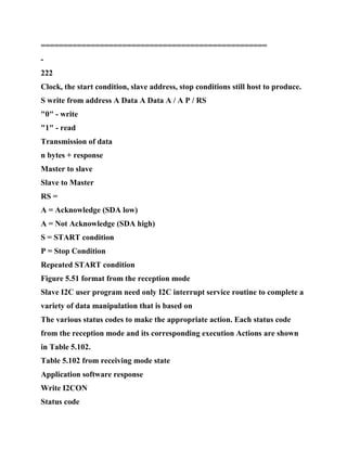
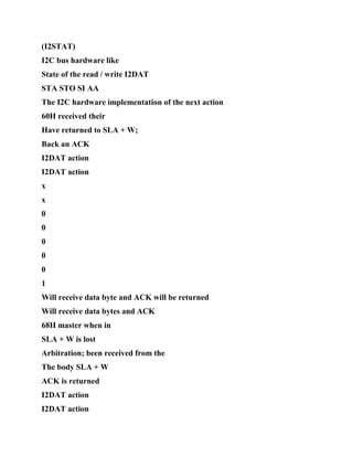
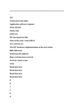
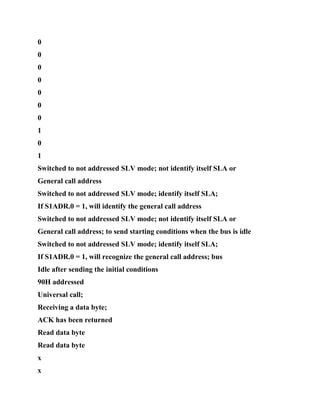
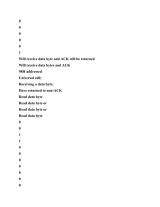

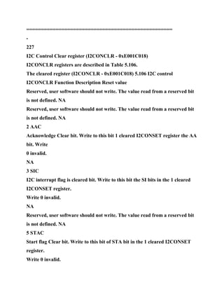
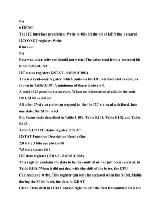
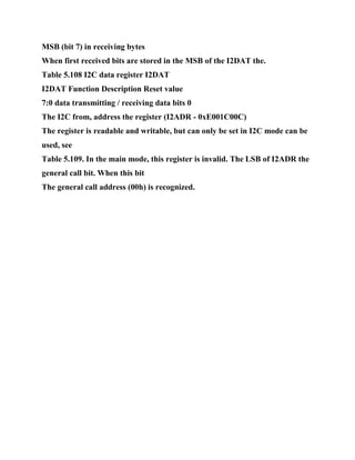
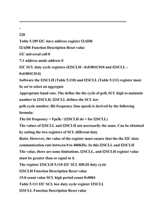
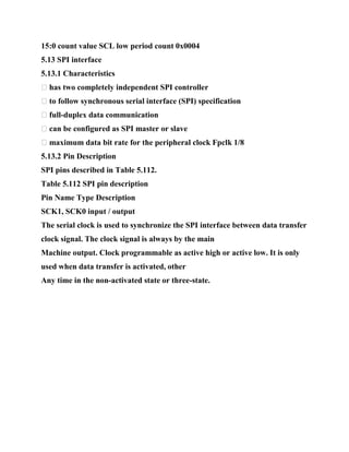
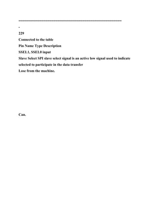


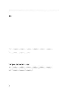


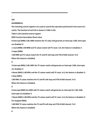
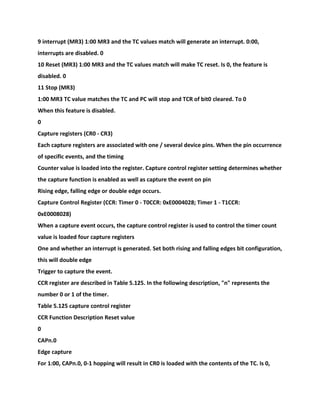
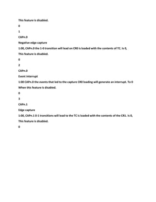
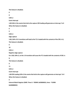
![External Match Register provides external the matching pin MATn.0 to MATn.3 (n is 0 or 1),
control and status.
The EMR register is described in Table 5.126.
Table 5.126 External Match Register
The EMR functional description reset value
0 external matching 0
MAT0.0/MAT1.0 whether connected to pin, this bit will reflect MAT0.0/MAT1.0 of
State. When MR0 match occurs, the output can be flipped to go low, go high
Or does not perform any action. Bit EMR [4:5] control the output of the function.
0
1 external matching 1
Regardless of the MAT0.1/MAT1.1 connected to pin, this bit will reflect MAT0.1/MAT1.1 of
State. When a when MR1 match occurs, the output can be flipped, goes low, goes high
Or does not perform any action. Bit EMR [6:7] to control the output of the function.
0
2 external matching
Regardless of MAT0.2/MAT1.2 is connected to a pin, this bit will reflect MAT0.2/MAT1.2
State. When the MR2 when a match occurs, the output can be flipped to go low, go high
Or does not perform any action. Bit EMR [8:9] control the output of the function.
0
3 external matching 3
Regardless of MAT0.3/MAT1.3 whether connected to the pin, this bit will reflect
MAT0.3/MAT1.3 of
State. When a match occurs, MR3 The output can be flipped to go low, go high
Or does not perform any action. Bit EMR [10:11] control the output of the function.
0
5:4
External matching
Control 0](https://image.slidesharecdn.com/armembeddedsystemessentialszlg-230111081204-4bc9ad56/85/ARM-Embedded-System-Essentials-ZLG-docx-655-320.jpg)
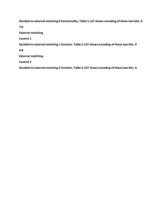
![==================================================
-
244
Connected to the table
The EMR functional description reset value
11:10
External matching
Control 3
Decided external matching 3 features. Table 5.127 shows encoding of these two bits. 0
Table 5.127 external matching control
EMR [11:10], EMR [9:8]
EMR [7:6], or EMR [5:4]
Function
00 does not perform any action
01 will match the corresponding external output is set to 0 (if connected to the pin, the
output low)
10 the corresponding external matching output is set to 1 (if connected to the pin, the output
high)
11 so that the corresponding external matching output flip
5.14.7 Timer example operation
Figure 5.59 shows a timer configured to reset the count and generate an interrupt on match.
Prescaler is set to 2, matching Send
The register is set to 6. The end of the match timer period, the timer count is reset. This has a
matching value
The full length of the cycle. Interrupt timer reaches the match value indicates a match under
a clock generator.
Figure 5.60 shows a timer configured to stop and generate an interrupt in the match.
Prescaler is set to 2 match registers
Is set to 6. TCR timer enable bit is cleared and generate instructions match timer reaches the](https://image.slidesharecdn.com/armembeddedsystemessentialszlg-230111081204-4bc9ad56/85/ARM-Embedded-System-Essentials-ZLG-docx-657-320.jpg)
![value of the next cycle of the match
With interrupt occurred.
pclk
Prescale Counter
Timer counter
Timer counter
Reset
Interrupt
201201201201
45601
Figure 5.59 timer period is set to PR = 2, MRx = 6 match enable interrupt and reset
TCR [0]
201
456
10
20
pclk
Prescale Counter
Timer counter
(Counter enable)
Interrupt
Figure 5.60 timer cycle setting is PR = 2, MRx = 6, enable interrupt and stop the timer match](https://image.slidesharecdn.com/armembeddedsystemessentialszlg-230111081204-4bc9ad56/85/ARM-Embedded-System-Essentials-ZLG-docx-658-320.jpg)
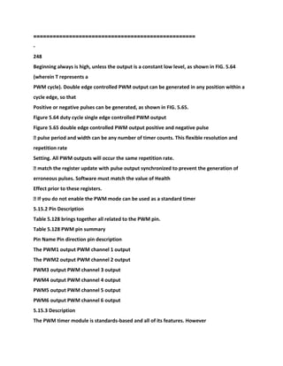
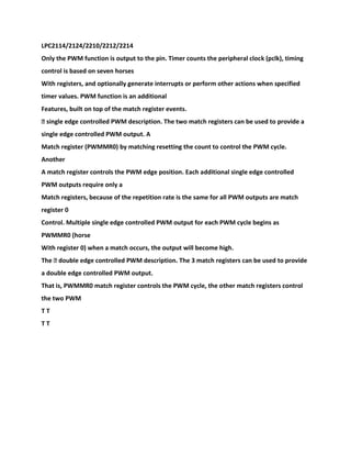
![M [6:0]
=
PWMSEL2
mux PWM2
PWMSEL3
mux PWM3
PWMSEL4
mux PWM4
PWMSEL5
mux PWM5
PWMSEL6
mux PWM6
PWM1
PWMENA1 .. 6 PWMSEL2 .. 6
S Q
R EN PWMENA1
S Q
R EN
S Q
R EN
S Q
R EN
PWMENA3
PWMENA2
PWMENA4
S Q
R EN PWMENA5
S Q
R EN PWMENA6](https://image.slidesharecdn.com/armembeddedsystemessentialszlg-230111081204-4bc9ad56/85/ARM-Embedded-System-Essentials-ZLG-docx-668-320.jpg)
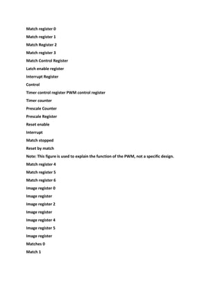
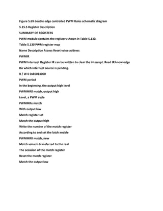
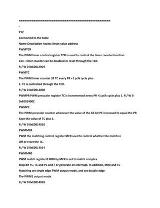

![(PWMMR0)
1:00, PWMMR0, with PWMTC value matching will enable PWMTC reset. To 0
When this feature is disabled.
0
2
Stop
(PWMMR0)
To will make PWMTC and PWMPC 1:00 PWMMR0, and PWMTC values match
Stop and PWMTCR [0] is reset to 0. Is 0, the feature is disabled.
0
3
Interrupt
(PWMMR1)
1:00, PWMMR1, and PWMTC value match will generate an interrupt. Is 0, the
Interrupts are disabled.
0
4
Reset
(PWMMR1)
1:00, PWMMR1, with PWMTC value matching will enable PWMTC reset. To 0
When this feature is disabled.
0
5
Stop
(PWMMR1)
To will make PWMTC and PWMPC 1:00 PWMMR1, and PWMTC values match
Stop and PWMTCR [0] is reset to 0. Is 0, the feature is disabled.
0
6](https://image.slidesharecdn.com/armembeddedsystemessentialszlg-230111081204-4bc9ad56/85/ARM-Embedded-System-Essentials-ZLG-docx-682-320.jpg)
![Interrupt
(PWMMR2)
1:00, PWMMR2, and PWMTC value match will generate an interrupt. Is 0, the
Interrupts are disabled.
0
7
Reset
(PWMMR2)
1:00, PWMMR2, with PWMTC value matching will enable PWMTC reset. To 0
When this feature is disabled.
0
8
Stop
(PWMMR2)
To will make PWMTC and PWMPC 1:00 PWMMR2, and PWMTC values match
Stop and PWMTCR [0] is reset to 0. Is 0, the feature is disabled.
0
9
Interrupt
(PWMMR3)
1:00, PWMMR3, and PWMTC value match will generate an interrupt. Is 0, the
Interrupts are disabled.
0
10
Reset
(PWMMR3)
1:00, PWMMR3, with PWMTC value matching will enable PWMTC reset. To 0
When this feature is disabled.
0](https://image.slidesharecdn.com/armembeddedsystemessentialszlg-230111081204-4bc9ad56/85/ARM-Embedded-System-Essentials-ZLG-docx-683-320.jpg)
![11
Stop
(PWMMR3)
To will make PWMTC and PWMPC 1:00 PWMMR3, and PWMTC values match
Stop and PWMTCR [0] is reset to 0. Is 0, the feature is disabled.
0
12
Interrupt
(PWMMR4)
1:00, PWMMR4, and PWMTC value match will generate an interrupt. Is 0, the
Interrupts are disabled.
0
13
Reset
(PWMMR4)
1:00, PWMMR4, with PWMTC value matching will enable PWMTC reset. To 0
When this feature is disabled.
0](https://image.slidesharecdn.com/armembeddedsystemessentialszlg-230111081204-4bc9ad56/85/ARM-Embedded-System-Essentials-ZLG-docx-684-320.jpg)
![==================================================
-
255
Connected to the table
PWMMCR Function Description Reset value
14
Stop
(PWMMR4)
To will make PWMTC and PWMPC 1:00 PWMMR4, and PWMTC values match
Stop and PWMTCR [0] is reset to 0. Is 0, the feature is disabled.
0
15
Interrupt
(PWMMR5)
1:00, PWMMR5, and PWMTC value match will generate an interrupt. Is 0, the
Interrupts are disabled.
0
16
Reset
(PWMMR5)
1:00, PWMMR5, with PWMTC value matching will enable PWMTC reset. To 0
When this feature is disabled.
0
17
Stop
(PWMMR5)
To will make PWMTC and PWMPC 1:00 PWMMR5, and PWMTC values match
Stop and PWMTCR [0] is reset to 0. Is 0, the feature is disabled.
0](https://image.slidesharecdn.com/armembeddedsystemessentialszlg-230111081204-4bc9ad56/85/ARM-Embedded-System-Essentials-ZLG-docx-685-320.jpg)
![18
Interrupt
(PWMMR6)
1:00, PWMMR6, and PWMTC value match will generate an interrupt. Is 0, the
Interrupts are disabled.
0
19
Reset
(PWMMR6)
1:00, PWMMR6, with PWMTC value matching will enable PWMTC reset. To 0
When this feature is disabled.
0
20
Stop
(PWMMR6)
To will make PWMTC and PWMPC 1:00 PWMMR6, and PWMTC values match
Stop and PWMTCR [0] is reset to 0. Is 0, the feature is disabled.
0
PWM control register (PWMPCR - 0xE001404C)
PWM control register is used to enable and select the type of each PMW channel. The
function of each bit in Table 5.134.
Table 5.134 PWM control register
PWMPCR Function Description Reset value
1:0 Reserved, user software should not write. The value read from a reserved bit is not
defined. NA
The 2 PWMSEL2 0:00, PWM2 select a single edge control mode control mode, select double
edge; 1:00. 0
The 3 PWMSEL3 0:00, PWM3 single edge control mode control mode, select double edge;
1:00. 0](https://image.slidesharecdn.com/armembeddedsystemessentialszlg-230111081204-4bc9ad56/85/ARM-Embedded-System-Essentials-ZLG-docx-686-320.jpg)


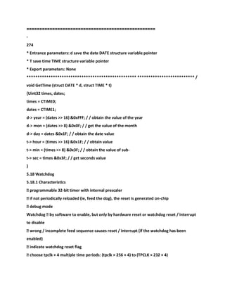
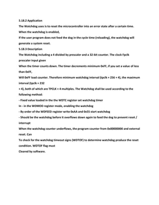
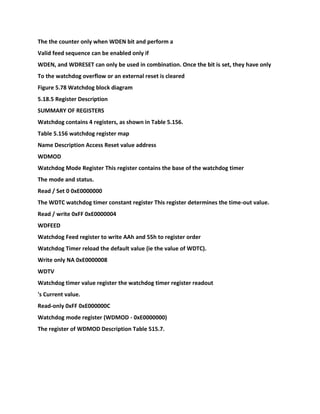
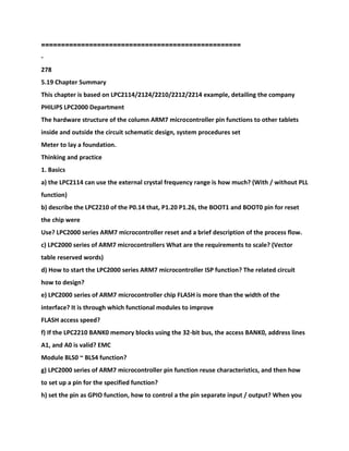
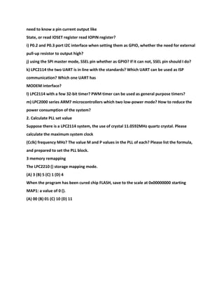
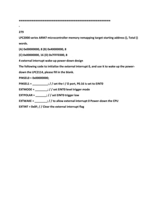
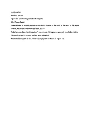
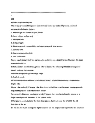
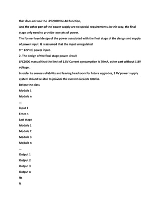

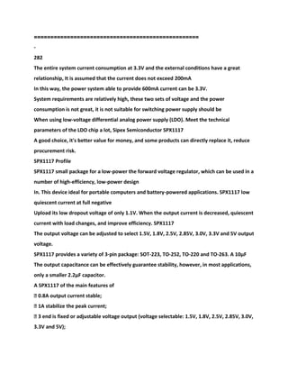

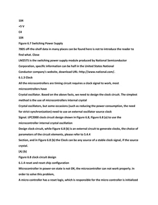
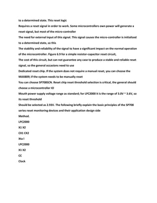
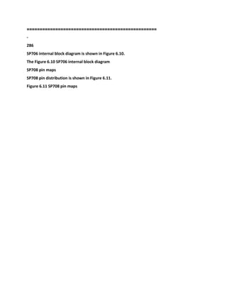
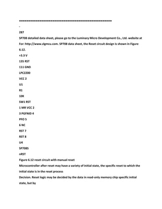


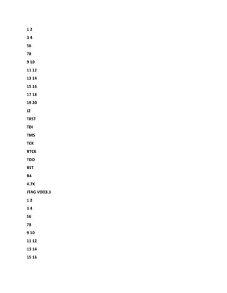
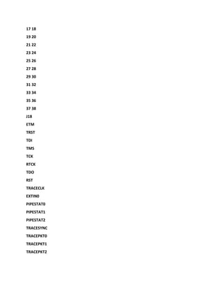
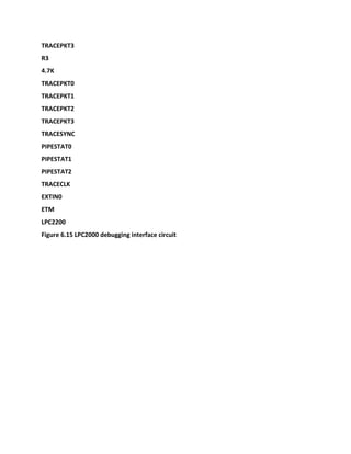
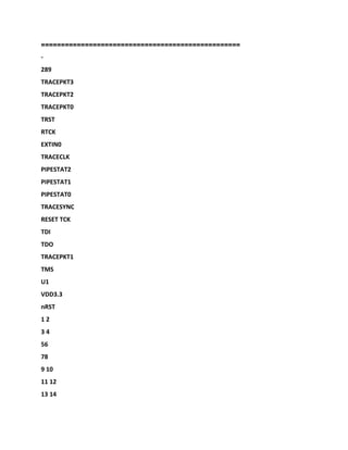
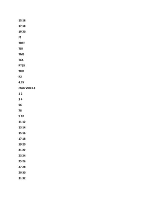
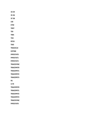


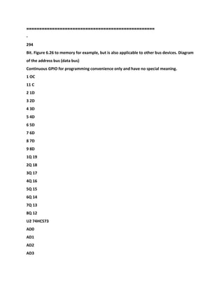

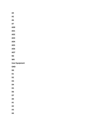
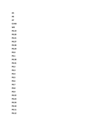
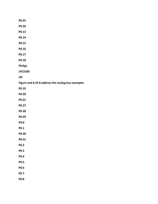
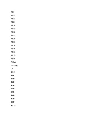
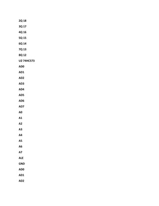

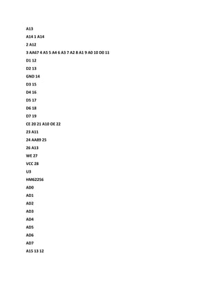
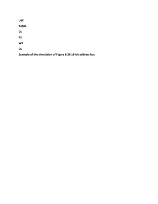

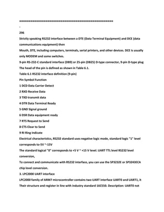
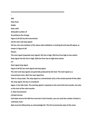
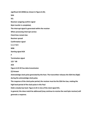
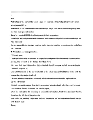
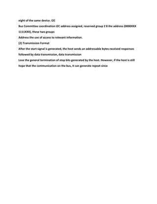
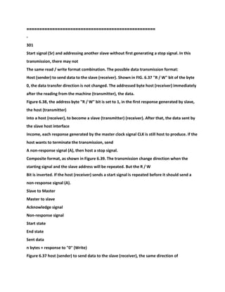
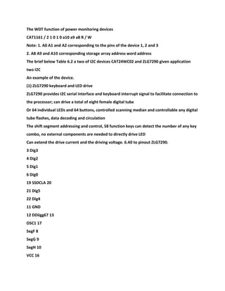
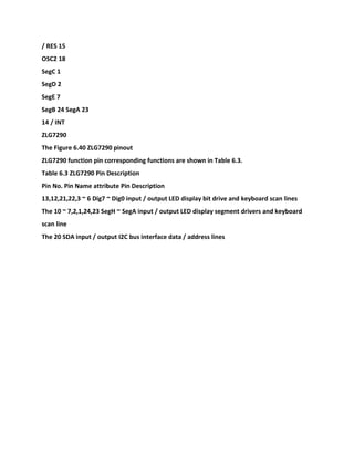
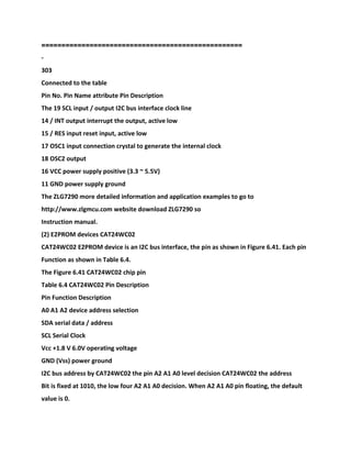
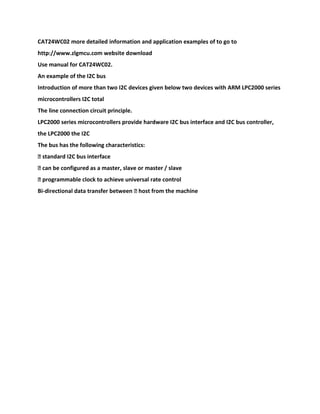
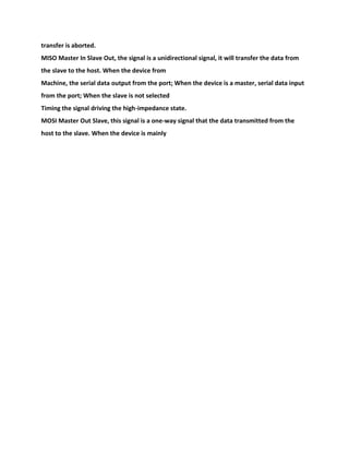
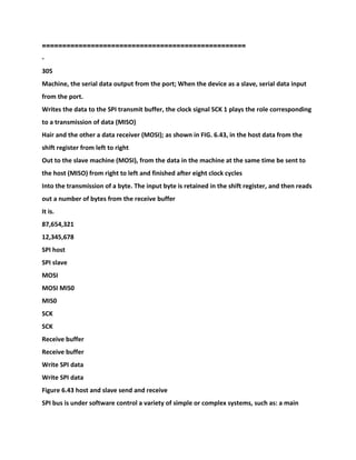
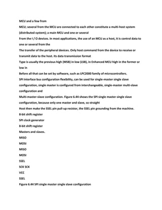
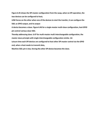
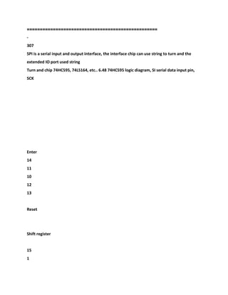


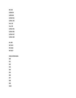


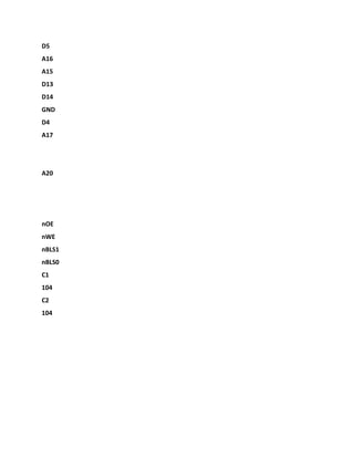


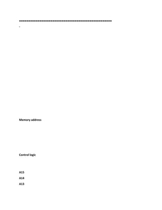


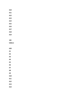
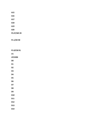


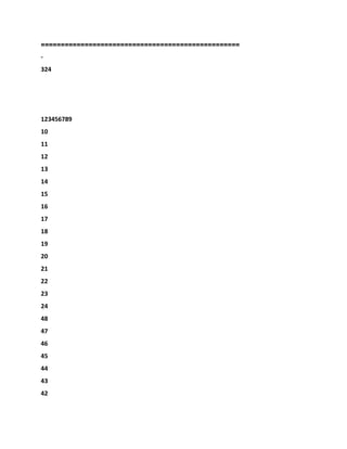


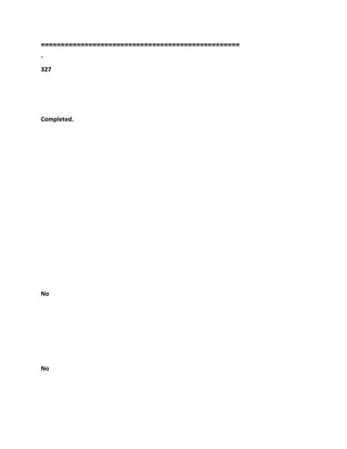

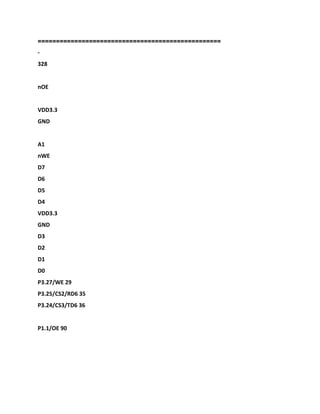


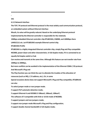
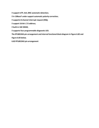
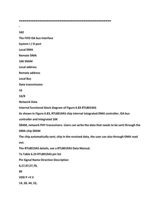
![83,86
GND P Land
34 AEN I address enable is "0", the I / O command is valid.
97-100,1-4 INT7-0 O interrupt request.
35 IOCRDY O is set to 0 to insert wait cycle to identify the host read and write commands.
96
IOCS16B
[SOLT16]
O
After power-on reset, RTL8019AS detects the pin to determine
Using the 16-bit or 8-bit ISA slots.
29 IORB I host read command.
30 IOWB I host write command.
The 33 RSTDRV I reset pin.
27-18,16-15,
13-7,5
SA19-0 I host address bus.
87-88,90-95,
43-36
SD15-0 I / O host data bus.
31 SMEMRB I host memory read command.
32 SMEMWB I host memory write command.
75 BCSB O BROM chip select.
The 76 EECS O 9346 chip select](https://image.slidesharecdn.com/armembeddedsystemessentialszlg-230111081204-4bc9ad56/85/ARM-Embedded-System-Essentials-ZLG-docx-942-320.jpg)
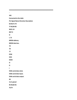
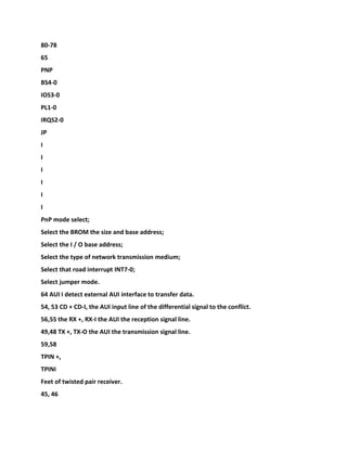
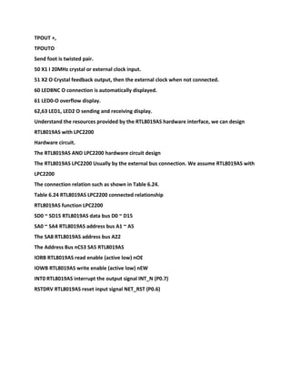
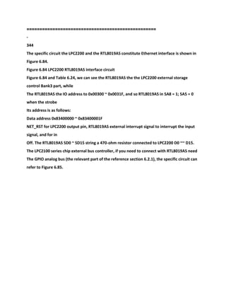
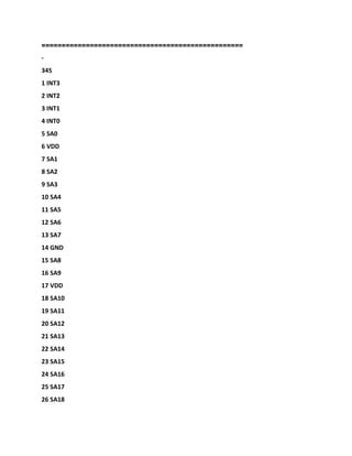
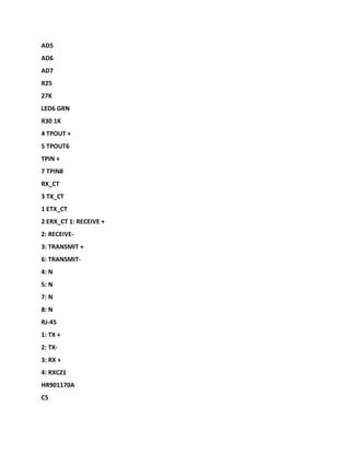
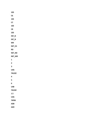
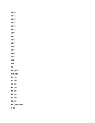
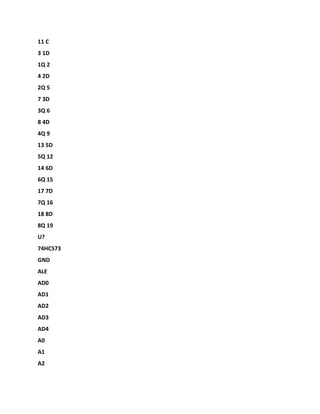
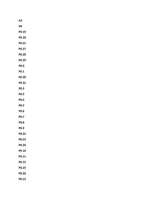
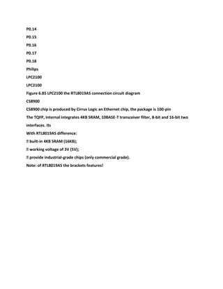
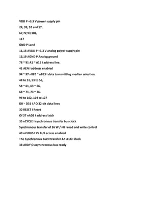
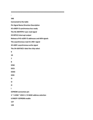
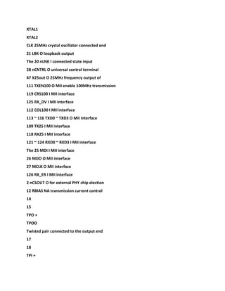
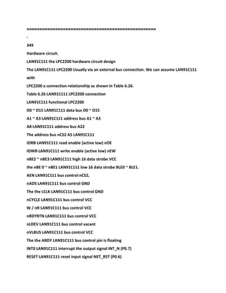
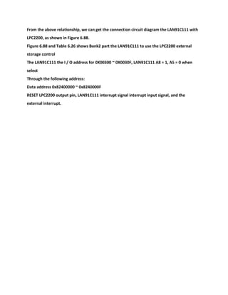
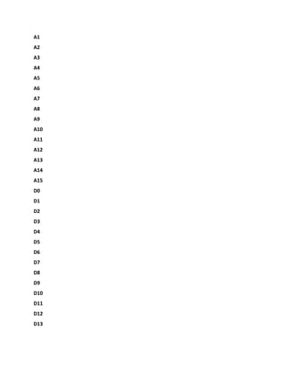
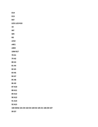
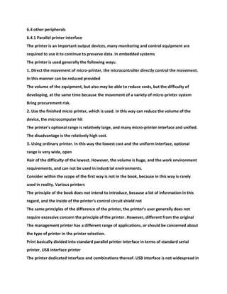

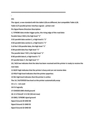
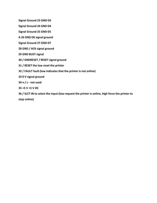
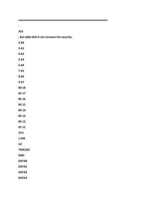
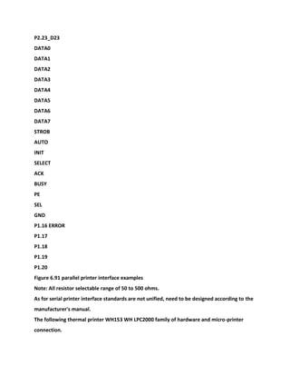
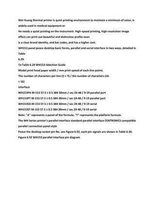
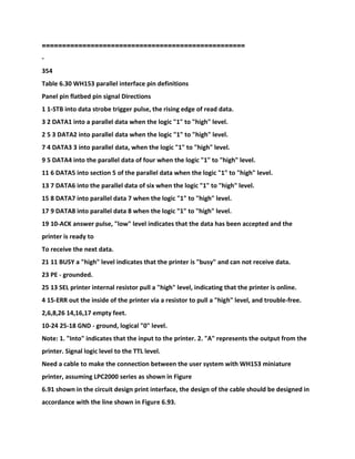
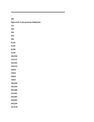
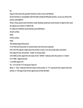
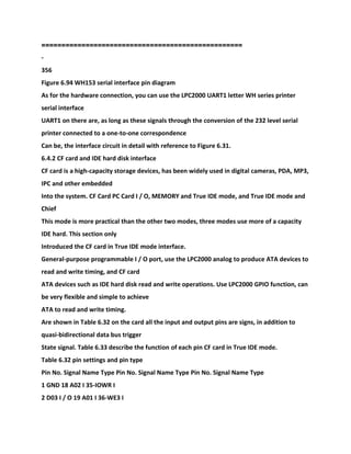
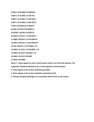
![==================================================
-
357
Table 6.33 CF card signal description
Signal names direction pin description
A2-A0 I 18,19,20 In True IDE mode, A [2:0] can be used to select the Task File (Task File) 8
One of the registers in the other address lines should be master is set to ground.
-PDIAG I / O 46 IDE real mode, the diagnostic signals via master / slave handshake protocol
input / output.
-DASP I / O 45 True IDE mode, disk boot / from disk ready signal via master / slave handshake
Association
Yee input / output.
Card detection pin grounding-CD1,-CD2 O 26,25 CF memory card and CF + card. They used to
be the master
Detect CF memory card and CF + card is fully inserted into the slot.
-CS0,-CS1
In True IDE mode, I 7,32-CS1 is used to select the auxiliary status register and device control
Register,-CS0 chip select signal task file register.
-CSEL
I 39 card internal signal control equipment; pull the pin when the pin is grounded, the device
is configured mainly
Mode, when the pin is empty, the device is configured for slave mode.
D15-D00
I / O 31,30,29,28,27
, 49,48,47,6,5,4
, 3,2,23,22,21
When all the data D [15:0] 16 transmission, the task file registers in
Bus low D [7:0] on the operation byte.
GND - 1,50 Ground.](https://image.slidesharecdn.com/armembeddedsystemessentialszlg-230111081204-4bc9ad56/85/ARM-Embedded-System-Essentials-ZLG-docx-986-320.jpg)

![Data (D15: D00)
-IOCS16
(See Note 3)
IORDY
(See Notes 4,4-1)
IORDY
(See Notes 4,4-2)
IORDY
(See Notes 4,4-3)
Figure 6.95 I / O timing diagram
Comment:
Device address-CS0,-CS1 and A [02:00] decision.
2 data from D [15:00] (16) or D [07:00] (8-bit).
3.-IOCS16 PIO modes 0, 1, 2, the other mode, the signal is ignored.
Equipment IORDY low to extend the PIO cycle. -IORD or-IOWR is provided tA time, the master
can be determined cycle
Is extended. IORDY described in the following three ways:
(1) The device never produce IODRY low level: no wait
(2) The equipment tA before driving IORDY is low, will enable IORDY in tA before set: no wait
(3) equipment in tA before start driving IORDY low: waiting for. IORDY is set again to
complete the cycle. In order week
Period
Generated within the waiting for the signal and set-the IORD tRD signal device will read data
is placed in before IORDY is set,
D15-D00.
LPC2000's GPIO pin CF card and IDE hard disk hardware wiring diagram in Figure 6.96 and
shown in Figure 6.97.
Table 6.36 LPC2210 GPIO pin CF card and IDE hard drive pin connection allocation table,
described in the table of](https://image.slidesharecdn.com/armembeddedsystemessentialszlg-230111081204-4bc9ad56/85/ARM-Embedded-System-Essentials-ZLG-docx-993-320.jpg)