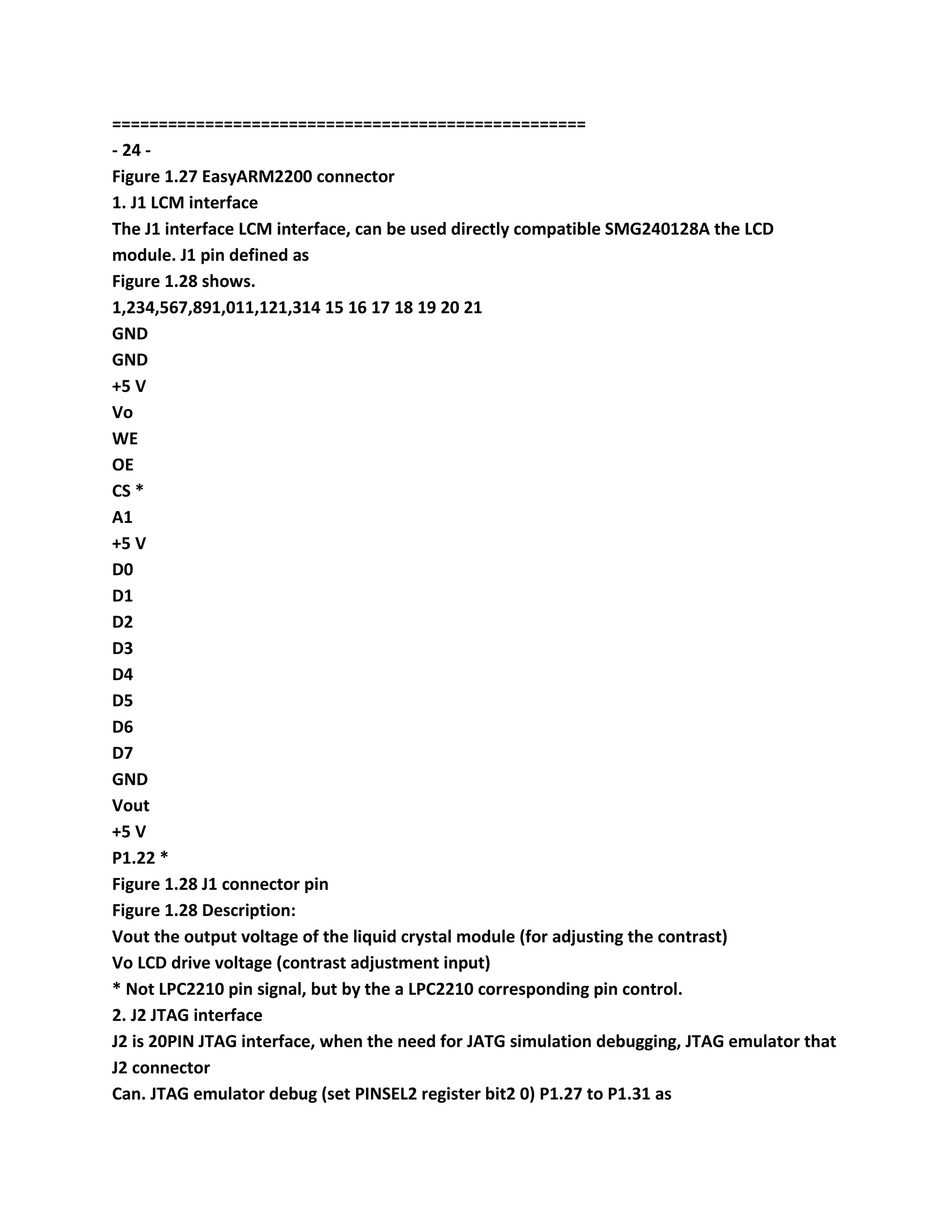
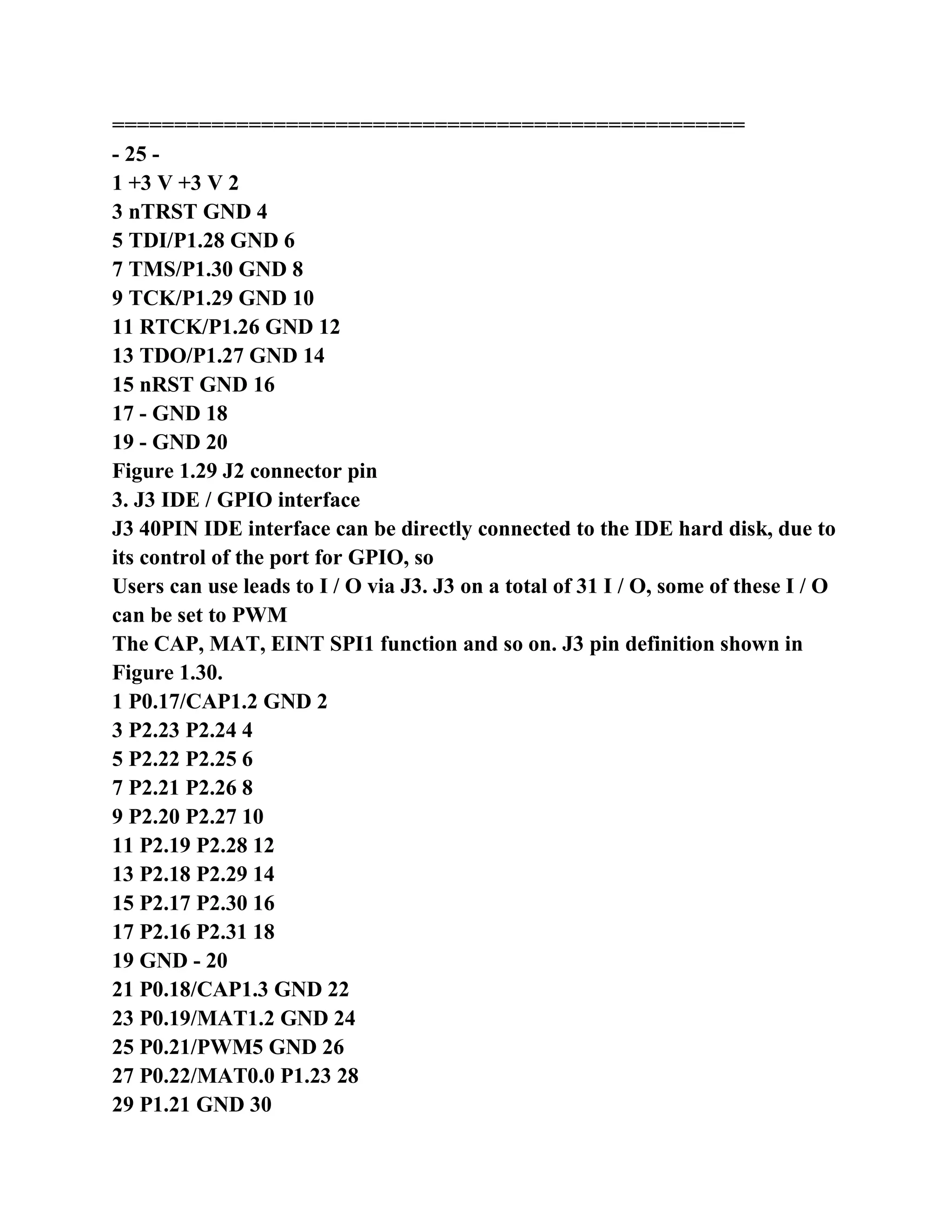
The document describes the hardware structure of the EasyARM2200 development board. It includes 1) the features of the board which support various ARM chips and peripherals, 2) the hardware principles including power supply, reset circuit, clock circuit and JTAG interface, 3) the hardware structure with component layout diagram and connector/jumper descriptions, and 4) use of hardware resources and other details like installation of CPU packs. It then introduces the ADS integrated development environment and EasyJTAG emulator application.


![===================================================
- 31 -
Figure 2.2 AXD debugger
The 2.2 engineering of editing
2.2.1 Establishing the works
WINDOWS operating system, click the [Start] -> [Programs] -> [ARM
Developer Suite v1.2] ->
[CodeWarrior for ARM Developer Suite] starting Metrowerks CodeWarrior,
or the double-"CodeWarrior
for ARM Developer Suite "shortcut starter start ADS1.2 IDE shown in Figure
2.3.
Figure 2.3 start ADS1.2 IDE
Click the [File] menu, select [New ...] pop-up New dialog box, shown in Figure
2.4.](https://image.slidesharecdn.com/arm1-230111081203-5f490f0b/75/ARM-1-docx-62-2048.jpg)
![===================================================
- 32 -
Figure 2.4 New dialog
Select the project template for ARM executable image (ARM Executable
Image) or Thumb executable mappings
(Thumb Executable Image), or the Thumb, ARM intertwined image (Thumb
ARM Interworking Image),
Storage path and in [Location options works, and in the [Project name] entry
input project name, click [indeed
Given] button to create the corresponding engineering project file name suffix
for mcp (hereinafter sometimes project called Project).
2.2.2 create documents
Create a text file, in order to enter the user program. Click "New Text File"
icon button, shown in Figure 2.5
Shows.
Figure 2.5 "New Text File" icon button
New file program, click on the "Save" icon button to save files (or from the
[File] menu options
Choose [Save]), the full name of the input file, such as TEST1.S. Note that,
save the file to the corresponding directory of the project,
Easy to manage and find.
Of course, you can also New dialog box, select [File] page to create a source
file, shown in Figure 2.4, or use other
A text editor to create or edit the source files.
2.2.3 Add file to project
In the project window, as shown in Figure 2.6 [Files] page blank space right
click pop-up floating menu, select "Add
Files ... "to pop up the" Select files to add ... "dialog box, select the
corresponding source file (subject Ctrl key election
Optional multiple files), click [open] button.
Project templates
Engineering the storage path
Project Name
New Text File](https://image.slidesharecdn.com/arm1-230111081203-5f490f0b/75/ARM-1-docx-63-2048.jpg)
![===================================================
- 33 -
In addition, users can select the [Project] menu [Add Files ...] to add the
source files, or use the New
Source file to create the dialog box, select [File] page, select the project (ie
select "Add to Project"). Add text
The parts operation shown in Figure 2.6, as shown in Figure 2.7.
Figure 2.6 add the source files in the project window
Figure 2.7 Select files to add ... dialog box
2.2.4 compiled connected engineering
These icons button icon button in the project window, shown in Figure 2.8,
you can quickly project set
Set, compiled connection start debugging (on a different menu items can find
the corresponding menu command). They left to
To the right, respectively, as follows:
DebugRel Settings ... project settings, such as the address set the output file
settings, such as compiler options,
In which DebugRel for the current generation target (target system).](https://image.slidesharecdn.com/arm1-230111081203-5f490f0b/75/ARM-1-docx-64-2048.jpg)
![===================================================
- 33 -
Synchronize Modification Dates sync each file modification date, modified
date, check the project if
Updates (such as the use of other editor to edit the source files), in
Touch column marked "√".
Make compile connection (shortcut key F7).
Debug start AXD debugging (shortcut key F5).
Run start AXD debug, and run the program directly.
The Project Inspector engineering checks, view and configure the project
source file.
Figure 2.8 project window icon button
Figure 2.9 DebugRel Settings window
Icon click "DebugRel Settings ..." button, you can project address set the
output file settings, compiled
Translation options, and so on, as shown in Figure 2.9. "ARM Linker" dialog
box to set the connection address, "Language Settings"
Set compiler compiler option.
View simple software debugging connection address settings can not click
directly on the project window "Make".
Standard button to complete the compilation connection. If compile error,
there will be a corresponding error message, double-click the error prompt
line information
Editing window that will use the source code line the cursor pointed out this
error, compiled connected to the output window in Figure 2.10 below.
Similarly,
You can find the appropriate command in the [Project] menu.](https://image.slidesharecdn.com/arm1-230111081203-5f490f0b/75/ARM-1-docx-65-2048.jpg)
![===================================================
- 34 -
Figure 2.10 compiled connected to the output window
As shown in Figure 2.11, Touch the bar to mark the file is compiled, if the "√"
indicates that the corresponding file required
To recompile. Touch bar for tag files are compiled, if the "√" indicates that
the corresponding files need to be renumbered
Translation. / Cancel symbol "√" can be set by clicking on the column
position or project directory *. Tdt file deletion
The entire project source files are marked with a "√".
The Make operation in Figure 2.11 Project window
2.2.5 Open the old engineering
Click [File] menu, select Open ...] that pop up the "Open" dialog box, find the
corresponding project file (*. Mcp)
Touch bar](https://image.slidesharecdn.com/arm1-230111081203-5f490f0b/75/ARM-1-docx-66-2048.jpg)
![===================================================
- 36 -
Click [Open]. Double-click the source file name to open the file in the project
window [Files] page
Edited.
The 2.3 engineering of debugging
2.3.1 Select the debug target
Figure 2.12 Choose Target window
When engineering compiled connected by click "Debug" icon button in the
project window, you can start AXD
Debug (You can also start] menu starting AXD). Click on the menu [Options]
select [the Configure Target ...]
Choose Target window pops up that, as shown in Figure 2.12. Add other
emulation driver, Target in
Only two were ADP (JTAG hardware simulation) and ARMUL (software
emulation).
Select emulation driver, click [File] Select [Load Image ...] the loaded ELF
format executable
Pieces, ie *. Axf file. Description: When engineering compiled connected by
the project name project name _Data current generated mesh
Standard "directory will generate a *. Axf debug files such as engineering the
TEST, the current generation of target Debug compile even
After connected, in ... the TEST TEST_Data Debug directory generate
TEST.axf file.
2.3.2 debug toolbar
AXD run debug tool bar as shown in Figure 2.13, debug observation window
toolbar shown in Figure 2.14, file operatives
Toolbar shown in Figure 2.15.
Figure 2.13 run debug toolbar
Running at full speed (Go)
Stop running (Stop)](https://image.slidesharecdn.com/arm1-230111081203-5f490f0b/75/ARM-1-docx-67-2048.jpg)


![===================================================
- 39 -
2.4.2 use the LPC2200 dedicated engineering template to establish engineering
Start ADS1.2 IDE, click [File] menu, select New ...] that is the pop-up New
dialog box, shown in Figure 2.18
Shown. Prior increase LPC2200 dedicated engineering template, so more
several engineering template selected in the project template column
Entry.
Figure 2.18 increase in the project template
LPC2200 special project templates are described as follows:
ARM Executable Image for lpc22xx: no operating system, all the C code is
compiled into the ARM instruction
Project template.
the asm for lpc22xx: Assembler project template.
Part of the C code the Thumb ARM Interworking Image for lpc22xx:
operating system compiled for ARM
Instruction, part of the C code is compiled for the the Thumb instruction of
project templates.
Thumb Executable Image for lpc22xx: No operating system all C compiled
into the Thumb instruction work
The process template.
ARM Executable Image for UCOSII (for lpc22xx): all the C code compiled for
ARM instruction
μC / OS-II project template
Thumb Executable Image for UCOSII (for lpc22xx): part of the C code is
compiled into the ARM instruction
Part of the C code is compiled for Thumb instruction μC / OS-II project
template (use the μC / OS-II, it is not possible to all code
Compiled into the Thumb instruction).
The user to select the appropriate project template building project, shown in
Figure 2.19 to use the ARM Executable Image for
lpc22xx project template to build a project. Works four generate the target
(target system): DebugInExram
The DebugInChipFlash, RelInChip RelOutChip, their configuration is shown
in Table 2.2. Project templates will phase](https://image.slidesharecdn.com/arm1-230111081203-5f490f0b/75/ARM-1-docx-71-2048.jpg)


![===================================================
- 41 -
; The initialization external bus controller, configured according to the target
board decided
LDR R0, = PINSEL2
IF: DEF: EN_CRP
LDR R1, = 0x0f814910
; 0x0f814910 changed to a desired value, note that the minimum 4 0
ELSE
LDR R1, = 0x0f814914
; 0x0f814914 changed to a desired value, if you use ETM last 4 need to be
modified to 6
ENDIF
STR R1, [R0]
LDR R0, = BCFG0
LDR R1, = 0x1000ffef
; 0x1000ffef changed values
STR R1, [R0]
LDR R0, = BCFG1
LDR R1, = 0x1000ffef
; 0x1000ffef changed values
STR R1, [R0]
......
3. Generate target DebugInExRam. Suppose the user systems chip debugging
the RAM usage bank0 (ie origin
Address is 0x8000 0000), this one can not be modified. If the user is not the
case, you can not use DebugInExRam
This generated a target debugger.
4. Generate target DebugInExRam. Assuming the user system in debug chip
RAM size is 512K bytes, this
Article affects only generate the target DebugInExRam. If not, you will need
to modify mem_b.scf this file, modify
Point, see the list of procedures 2.2. Note: the windows will hidden this file
extension, only for mem_b.
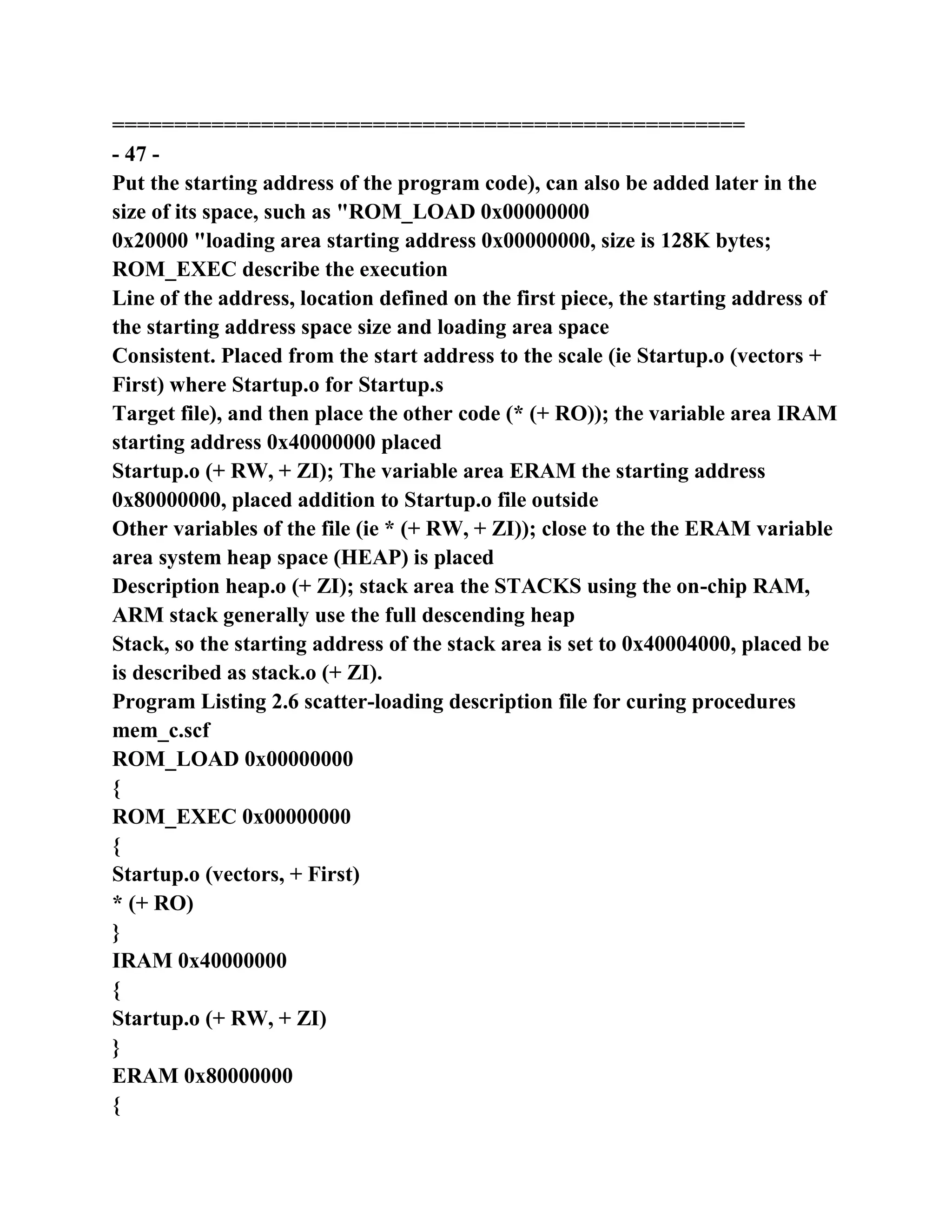
Program Listing 2.2 mem_b.scf file need to modify the code](https://image.slidesharecdn.com/arm1-230111081203-5f490f0b/75/ARM-1-docx-75-2048.jpg)


![===================================================
- 44 -
The emulator Figure 2.20 EasyJTAG the physical appearance
To 2.5.1 installed EasyJTAG emulator
First of all, the driver of the EasyJTAG emulator (like product CD
EasyJTAG_drive directory all files
Pieces) to the ADS BIN directory, such as C: Program Files ARM
ADSv1_2 BIN.
Then, the EasyJTAG emulator's 25-pin interface connected via a parallel port
extension cord with the parallel port of a PC,
EasyJTAG emulator 20-pin interface development boards J2 EasyARM2200
received by 20 PIN connection cable
Matching transformer (9V) power supply to the development board.
Then enter AXD debug environment, open the [Options] -> [Configure Target
...] to pop up the Choose Target
Window, as shown in Figure 2.12. Click "ADD" to add the emulator driver in
the Add File window choose, such as C: Program
Files ARM ADSv1_2 BIN directory EasyJTAG.dll, click "Open".
Description: Windows system, click [start] -> [Programs] -> [ARM Developer
Suite v1.2] ->
【The AXD Debugger】 can run AXD software directly.
Note: Add Files window displays DLL file, set the the WINDOWS file browser
window "file
Folder Options (O) ... "," hidden files "View page items using the" Show All
Files ".
And 2.5.2 use EasyJTAG emulator
Computer parallel port with EasyJTAG of emulator connection and emulator
JTAG port connector into EasyARM2200
Development board J2 AXD software is set to simulation debugging.
1 emulator settings
AXD debugging environment, open the [Options] -> [Configure Target ...]
Choose Target window pops up,
"Target Environments" box, select "EasyJTAG ..." item.
Click the "Configure" button, enter "EasyJTAG Setup" settings window, as
shown in Figure 2.21. "ARMcore"](https://image.slidesharecdn.com/arm1-230111081203-5f490f0b/75/ARM-1-docx-81-2048.jpg)
![Select the CPU type, select the "Options" item Halt and reset. Then click
"OK", and then click on the "OK"
The connection (development board) operation will be carried out at this time
EasyJTAG. If the connection is successful, the development board LPC2210
chip
EasyJTAG control, the previously running program is stopped.
Note: Sometimes, AXD will pop up an error dialog box as shown in Figure
2.23, or a similar dialog box can
Click "Connect mode ...", and then select the "ATTACH ..." to determine,
and then click "Restart". If EasyJTAG
Correctly connected to the development board, AXD code window will display
a blank, then you can use [File] -> [Load Image ...]
Debug file is loaded, JTAG debug.](https://image.slidesharecdn.com/arm1-230111081203-5f490f0b/75/ARM-1-docx-82-2048.jpg)
![===================================================
- 45 -
Figure 2.21 "EasyJTAG Setup" settings window
EasyJTAG set Option Description:
ARMcore items, select CPU model;
Tap No. Items, when the CPU for LPC2106/2105/2104, master / slave JTAG
debug port, Tap1 main
Tap2 from;
Connection, hardware connection interface options;
Halt Mode, the shutdown mode selection contains Halt program (to stop CPU)
and Halt and reset (reset and then stopped
Stop CPU) two;
Aux. Option, support options, including Step In Interrupt (allows single step
into the interrupt) and Erase Flash
when need (allow EasyJTAG Erase Flash) two;
Flash Type, chip FLASH Model Select two FLASH chip, when ARMcore
choose LPC2200
Series CPU this to be effective. When the program needs to be downloaded to
the chip FLASH, EasyJTAG emulator will be selected core
Model of chip erase / program.
Flash 0 Addrss, the first piece of Flash address set contains the Start Address
(Flash the start address, such as
Bank0 0x80000000) Memory Size (memory capacity when fill in the actual
chip capacity, such as
The capacity of the SST39VF160 0x200000). When the program do not need
to download to the chip FLASH, or the system does not chip
When FLASH, Start Address and Memory Size is set to 0.
The Flash 1 Addrss, with Flash 0 Addrss.
2 emulator application
Press F5 or Debug icon button to ADS1.2 IDE environment directly into AXD,
but sometimes appear as
Prompt shown in Figure 2.22, the processing method is to click "OK", and
then click the "Load Session window pop-up to take
Elimination. "Into AXD After, the main debug window without any code, and
[File] -> [Load Image ...] menu item without](https://image.slidesharecdn.com/arm1-230111081203-5f490f0b/75/ARM-1-docx-83-2048.jpg)
![Efficiency, the need to re-open the [Options] -> [Configure Target ...] Click
the "OK", and then click [File]
Select Load Image ...] to load the debug files.](https://image.slidesharecdn.com/arm1-230111081203-5f490f0b/75/ARM-1-docx-84-2048.jpg)
![===================================================
- 46 -
Figure 2.22 session file error
AXD debug environment, sometimes the Fatal AXD Error window pops up,
as shown in Figure 2.23, then you can
To click on the "Connect mode ...", and then select the "ATTACH ..." to
determine, and then click "Restart". Next on
Can use [File] -> [Load Image ...] loaded debug files for JTAG debugging.
Note: for some of the PC, EasyJTAG not correctly connected to the
development board, always error dialog box pops up, then can be
To check the parallel port connection is reliable, check whether the parallel
port on the dongle is connected to, or to re-development board under electric.
In addition,
CMOS settings in the PC parallel port mode is set to SPP mode, set the
parallel port of the resources for the 378H to 37FH.
Figure 2.23 Fatal AXD error
Chip peripheral registers observation. To open in the System Views] ->
[Debugger Internals] LPC2000
Series ARM7 microcontroller chip peripheral register window. Some registers
are not allowed to deliver the show or read operation will affect
The value of other registers, so can not be found in the on-chip peripheral
register window, if you need to observe these registers can be
Use of the the memory observation window (Memory).
JTAG download the program to the FLASH. Enter the AXD debugging
environment, open the [Options] -> [Configure
Target ...] Choose Target window pops up, click on the "Configure" button to
enter the set of "EasyJTAG Setup"
Window, select "FLASH" item "Erase Flash when need", then OK to exit. In
this way, each loaded FLASH
Address debug files, erase the FLASH and download code to FLASH.
2.6 firmware
To download the program to the on-chip FLASH FLASH or external JTAG
emulator debug through (ie curing
Program), before they can run offline.
2.6.1 chip FLASH curing](https://image.slidesharecdn.com/arm1-230111081203-5f490f0b/75/ARM-1-docx-85-2048.jpg)


![===================================================
- 53 -
Chapter 3 Basic Experiment
The 3.1 ADS 1.2 integrated development environment to practice
3.1.1 The purpose of the experiment
Learn to use ADS 1.2 integrated development environment.
3.1.2 The laboratory equipment
� Hardware: PC, a
� software: Windows98/XP/2000 system, ADS 1.2 integrated development
environment
3.1.3 Experimental content
1 to create a new project;
2 Create a C source file, and added to the project;
Set compiler Connection control options;
4. Compile connection works.
3.1.4 prelab requirements
Carefully read the content of Section 2.2 of the book section ADS project
editor.
3.1.5 Experimental Procedure
1 start ADS1.2 IDE integrated development environment, select [File] -> [New
...] ARM Executable Image
The project template to create a project, project name for the ADS, as shown
in Figure 3.1.
Figure 3.1 build ARM instruction code works
2 Select [File] -> [New ...] a new file TEST1.S, the settings directly added to
the project, see
Figure 3.2. Enter the code shown in Listing 3.1 and save it, as shown in Figure
3.3.](https://image.slidesharecdn.com/arm1-230111081203-5f490f0b/75/ARM-1-docx-95-2048.jpg)

![===================================================
- 55 -
3 Select [Edit] -> [DebugRel Settings ...], the left side of the DebugRel Settings
dialog box, select the ARM
Linker item, then set in the Output page the connected address (see Figure
3.4), debug entry address set in the Options page (see Figure
3.5).
Figure 3.4 project to connect the address set
Figure 3.5 project commissioning entry address set
4 Select [Project] -> [Make], compiled connect the whole project.
3.1.6 Thinking
What is the role of project templates? (Hint: Compile control settings)
How to force re-compile all files of the project? (Hint: select [Project] ->
[Remove Object Code ...]
The deleted engineering in the *. Obj file)](https://image.slidesharecdn.com/arm1-230111081203-5f490f0b/75/ARM-1-docx-97-2048.jpg)

![Port address Image entry point 0x40000000.
Compile the connection works, select [Project] -> [Debug], start AXD
software simulation debugging.
Open the register window (Processor Registers), the Select Current
monitoring R0, the value of R1. Open storage
Is observation window (Memory) setting observed address as 0x40003100
Pattern Size 32Bit monitoring
0x40003100 address value.
Description: Memory window, click the right mouse button, select the display
format for 8Bit, 16Bit, 32Bit Size item.
Shown in Figure 3.6.
Can single-step run the program, you can set / cancel the breakpoint, or run
the program at full speed, stop the program running, debugging
Observed when the value on the address registers and 0x40003100. The
results are shown in Figure 3.7.](https://image.slidesharecdn.com/arm1-230111081203-5f490f0b/75/ARM-1-docx-99-2048.jpg)

![===================================================
- 58 -
AREA Example2, CODE, READONLY; declarative code segment Example2
ENTRY; identification program entry
CODE32; Statement 32-bit ARM instruction
START LDR R1, = COUNT; R1 <= COUNT
MOV R0, # 0; R0 <= 0
STR R0, [R1]; [R1] <= R0, that set COUNT 0
LOOP LDR R1, = COUNT
LDR R0, [R1]; R0 <= [R1]
ADD R0, R0, # 1; R0 <= R0 + 1
CMP R0, # 10; R0 and 10 comparison, affect the condition code flags
MOVHS R0, # 0; If R0 is greater than or equal to 10, this instruction is
executed, R0 <= 0
STR R0, [R1]; [R1] <= R0, ie save COUNT
B LOOP
END
3.2.7 Thinking
If instead of the program in Listing 3.2 LDRB / STRB load / store instructions
(LDR / STR), the program will be
Correct execution?
LDR pseudo-instruction LDR load instruction features and applications
What's the difference between an example? (Hint: LDR directive
The form of a "LDR Rn, = expr")
LDR / STR instructions before index offset instructions how to write?
Instructions how to operate?
The AXD debugger how to reset program? (Hint: Select [File] -> [Reload
Current Image] re-add
Upload image files)
3.3 assembly instructions experimental 2
3.3.1 The purpose of the experiment
1 to master the use of the ARM data processing instruction;
Learn the ARM instruction flexible two operands.
3.3.2 The laboratory equipment
� Hardware: PC, a](https://image.slidesharecdn.com/arm1-230111081203-5f490f0b/75/ARM-1-docx-101-2048.jpg)

![===================================================
- 59 -
3.3.4 prelab requirements
Carefully read Chapter 4 ARM "ARM based embedded system tutorial
instruction system;
Carefully read the contents of the book Edit 2.2, 2.3 section of ADS project
and AXD debugger. (The experimental use software emulation)
3.3.5 Experimental Procedure
Start ADS 1.2, to use ARM Executable Image project template to create a
project Instruction2.
2. Establish assembler source file TEST3.S, the preparation of the
experimental procedure, and then added to the project.
Set works connected address RO Base 0x40000000, RW Base for 0x40003000.
Set debug into
Port address Image entry point 0x40000000.
Compile the connection works, select [Project] -> [Debug], start AXD
software simulation debugging.
Open the register window (Processor Registers), select Current Item
monitoring the value of the register.
Description: Use the left mouse button to select a register, and then click the
right mouse button, choose to display the Format item
Format Hex, Decimal, and so on. Shown in Figure 3.8.
Figure 3.8 setting register display format
6 single-step run the program and observe the changes of register values.
Description: change registers will be displayed in red. Figure 3.9.](https://image.slidesharecdn.com/arm1-230111081203-5f490f0b/75/ARM-1-docx-103-2048.jpg)


![===================================================
- 62 -
Register (R2) for counting the cycle n-1 times R0 = R0 * R1, the operation
result is stored in R0. (Without regard to the results of overflow
Problems)
Note that, if n is 0, then the calculation result is assigned directly 1; if n is 1,
then the result of the operation assigned directly to X.
3.4.6 Experimental Procedure
Start ADS 1.2, to use ARM Executable Image project template to create a
project Instruction3.
2. Establish assembler source file TEST4.S, the preparation of the
experimental procedure, and then added to the project.
Set works connected address RO Base 0x40000000, RW Base for 0x40003000.
Set debug into
Port address Image entry point 0x40000000.
Compile the connection works, select [Project] -> [Debug], start AXD
software simulation debugging.
Open the register window (Processor Registers), select Current monitoring
registers R0, R1, R13 (SP)
And the value of R14 (LR).
6 open the memory observation window (Memory) settings observed address
0x40003EA0, and Display Size is
32Bit, monitored from 0x40003F00 starting full descending stack area.
7. Single-step run the program, the process of tracking program execution,
observation register values change and the stack area data changes
Judge the execution result is correct.
Debugger, change the parameters X and n test program to observe whether or
not to get the correct result. For example: the first complex
Bit program (select [File] -> [Reload Current Image]), followed by single-step
execution to "BL POW"
Instructions, modify the value in the register window R0, R1, and then
continue to run the program.
Description: register register window, double-click with the mouse, you can
modify the value of the register. The input data can be decimal
Number (136,198), can also be a hexadecimal number (such as 0x123 That will](https://image.slidesharecdn.com/arm1-230111081203-5f490f0b/75/ARM-1-docx-107-2048.jpg)


![Compile the connection works, select [Project] -> [Debug], start AXD
software simulation debugging.
Open the register window (Processor Registers), select Current Item
monitoring the value of the register.
6 single-step run the program, pay attention to the implementation of the BX
R0 instruction before and after the CPSR T bit.
Description: in register window CPSR register, the bit representation of the
uppercase letters bit of the bit is 1, lowercase letters
This bit is 0 (such as "T" T bit to 1, "t", said the T bit is 0).
3.5.7 experimental reference program
Assembly instructions, experiment 4 reference code shown in Listing 3.5.
The program list 3.5 assembly instructions experimental reference program
; The file name: TEST5.S
; Function: computing 1 +2 + ... + the value of N
;: N ≥ 0, N = 0, the result is 0; When N = 1, the result is 1.
N EQU 100; define the value of N is 100
AREA Example5, CODE, READONLY; declarative code segment Example5](https://image.slidesharecdn.com/arm1-230111081203-5f490f0b/75/ARM-1-docx-112-2048.jpg)


![3. Establish assembler source file TEST6.S, the preparation of the
experimental procedure, and then added to the project.
Set works connected address RO Base 0x40000000, RW Base for 0x40003000.
Set debug into
Port address Image entry point 0x40000000.
5. Compile the connection works, select [Project] -> [Debug], start AXD
software simulation debugging.
Open the register window (Processor Registers), select Current Item
monitoring the value of the register.
7. Single-step run the program to determine whether the implementation of
the program logic design.
3.6.6 experimental reference program
5 assembly instruction experiment reference program shown in Listing 3.6.
The program list 3.6 assembly instructions experimental reference program
AREA Example6, CODE, READONLY; declarative code segment Example6
ENTRY; identification program entry
CODE32; Statement 32-bit ARM instruction
START; if (x> y) z = 100;](https://image.slidesharecdn.com/arm1-230111081203-5f490f0b/75/ARM-1-docx-116-2048.jpg)


![Carefully read the contents of the book Edit 2.2, 2.3 section of ADS project
and AXD debugger. (The experimental use software emulation)
3.7.5 Experimental Procedure
Start ADS 1.2, ARM Executable Image project template to establish an
engineering MODE.
2. Establish assembler source file TEST7.S, the preparation of the
experimental procedure, and then added to the project.
Set works connected address RO Base 0x40000000, RW Base for 0x40003000.
Set debug into
Port address Image entry point 0x40000000.
Compile the connection works, select [Project] -> [Debug], start AXD
software simulation debugging.
Open the register window (Processor Registers), select Current Item
monitoring the value of the register.
6 single-step run the program, observe the CPSR, SPSR, R13 (SP), R14 (LR),
R15 (PC) register.
Description: CPSR register display as shown in Figure 3.10. Display is divided
into two parts, the part of the respective flag bit,
The other part is the working mode.
Flag NZCVQ condition code flags N, Z, C, V, Q, capital letters, this bit is 1;
significant](https://image.slidesharecdn.com/arm1-230111081203-5f490f0b/75/ARM-1-docx-122-2048.jpg)


![===================================================
- 74 -
5. Compile the connection works, select [Project] -> [Debug], start AXD
software simulation debugging.
6 to set a breakpoint. In Startup.S the "B Main" at the program and then
moving full-speed line.
7. Program stops at the breakpoint. Single-step run the program, to determine
whether the program jumps to the C program running.
8. Choose [Processor Views] -> [Variables]) Open variable observation
window to observe the value of the global variable
Single step / run programs at full speed, the calculation result of the judgment
program is correct.
3.8.6 Experimental reference program
C language experiment reference program shown in Listing 3.8. Compilation
starter code shown in Listing 3.6.
Program in Listing 3.8 C language experiment reference program
# Define uint8 unsigned char
# Define uint32 unsigned int
# Define N 100
uint32 sum;
/ / Use the adder to calculate the 1 +2 +3 + ... + (N-1) + N of values. (N> 0)
void Main (void)
{Uint32 i;
sum = 0;
for (i = 0; i <= N; i + +)
{Sum + = i;
}
while (1);
}
3.9 simple starter code for program listings
; Starter file. Initialize the runtime environment of the C program, and then
enter the C code.
IMPORT | Image $ $ RO $ $ Limit |
IMPORT | Image $ $ RW $ $ Base |
IMPORT | Image $ $ ZI $ $ Base |](https://image.slidesharecdn.com/arm1-230111081203-5f490f0b/75/ARM-1-docx-129-2048.jpg)

![===================================================
- 75 -
LDR R0, = | Image $ $ RO $ $ Limit |
LDR R1, = | Image $ $ RW $ $ Base |
LDR R3, = | Image $ $ ZI $ $ Base |
CMP R0, R1
BEQ LOOP1
LOOP0 CMP R1, R3
LDRCC R2, [R0], # 4
STRCC R2, [R1], # 4
BCC LOOP0
LOOP1 LDR R1, = | Image $ $ ZI $ $ Limit |
MOV R2, # 0
LOOP2 CMP R3, R1
STRCC R2, [R3], # 4
BCC LOOP2
B Main; jump to C code Main () function
END
3.8.7 Thinking
The experimental reference program, Startup.S file is it? If no Startup.S file,
C programs will be delivered
Line make a mistake?
Experimental program in the Main () function name can be changed to
another name? (Hint: Main is just a label)
3.9 C language calling assembler experimental
3.9.1 The purpose of the experiment
Lies in the C language program call assembler, to understand ATPCS the
basic rules.
3.9.2 The laboratory equipment
� Hardware: PC, a
� software: Windows98/XP/2000 system, ADS 1.2 integrated development
environment
3.9.3 Experimental content
Assembly subroutine call in a C program, the addition of two integers. The
assembler subroutine prototype for:](https://image.slidesharecdn.com/arm1-230111081203-5f490f0b/75/ARM-1-docx-131-2048.jpg)

![===================================================
- 76 -
3.9.5 Experimental Procedure
Start ADS 1.2, to use ARM Executable Image project template to create a
project ProgramC1.
2. The source file Startup.S, Add.S and Test.c preparation of the experimental
procedure, and then added to the project.
Set works connected address RO Base 0x40000000, RW Base for 0x40003000.
Set debug into
Port address Image entry point 0x40000000.
4 setting works connectivity options, the initial code segment is set to the start
position Startup.o the Start segment.
5. Compile the connection works, select [Project] -> [Debug], start AXD
software simulation debugging.
6. The Test.c file call the Add () code sets a breakpoint at line program, then
full-speed action.
7. Program stops at the breakpoint. Use the Setp In single-step run the
program, observe the procedures Go assembler Add.S.
8. Choose [Processor Views] -> [Variables]) Open variable observation
window to observe the value of the global variable
Single step / run programs at full speed, the calculation result of the judgment
program is correct.
3.9.6 experimental reference program
C language calling assembler experiment reference program shown in Listing
3.10. Assembler the addition function code, see the list of procedures
3.11.
The program listing 3.10 C language calling assembler experimental reference
program
# Define uint8 unsigned char
# Define uint32 unsigned int
extern uint32 Add (uint32 x, uint32 y);
uint32 sum;
/ / Call to assembler Add realize the addition
void Main (void)
{Sum = Add (555, 168);](https://image.slidesharecdn.com/arm1-230111081203-5f490f0b/75/ARM-1-docx-133-2048.jpg)


![BeepCon_C.
Establishing C source file BeepCon.c, preparation of the experimental
procedure, and then added to the engineering of the user group.
5. Optional DebugInExram generation target, shown in Figure 3.12, and then
compile the connection works.
Figure 3.12 choose to generate the target
6. EasyARM2200 development board JP9 a short jumper, JP4 jumper off JP6
jumper settings
Bank0-RAM, Bank1-Flash.
7 Select [Project] -> [Debug] start AXD JTAG emulator debugging (emulator
need to be set up correctly.](https://image.slidesharecdn.com/arm1-230111081203-5f490f0b/75/ARM-1-docx-138-2048.jpg)
![===================================================
- 79 -
Refer to Section 2.5).
Note: Use DebugInExram generate the target, the use of off-chip RAM
simulation debugging JP6 jumper to be set up
Home for Bank0-RAM, Bank1-Flash, set in AXD emulator Reference shown
in Figure 3.13.
Figure 3.13 RAM chip debugging emulator set
JTAG connection error or AXD main window no display Startup.S source,
press book 2.5 referral
Deal with Shao methods.
Program run at full speed, the program will stop at the main function of
beepcon.c (because the main function at the beginning of the default
Set breakpoints).
Click Context Variable icon button (or select [Processor Views] ->
[Variables]) open change
The amount of observation window, local variables and global variables can
be observed through this window. Select System Views】 ->
The】 【Debugger Internals to open LPC2000 series ARM7 microcontroller
chip peripheral register window
Mouth.
11 can be a single-step run the program, you can set / cancel the breakpoint,
or run the program at full speed to stop the program running, observe
The value of a variable, it is judged whether the buzzer control correctly.
12 closed simulation debugging through AXD, ADS 1.2 integrated
development environment chosen RelOutChip generated mesh
Standard, and then compile the connection works.
13. EasyARM2200 development board JP9 a short jumper, JP1, JP4 jumper
disconnected JP6 jumper settings
Bank0-Flash, Bank1-RAM, JP7 jumper settings OUTSIDE.
14 Select [Project] -> [Debug] start AXD JTAG emulator debugging. At this
point EasyJTAG simulation
Will download the program to the chip FLASH emulator (need to be set up
correctly, refer to section 2.5).](https://image.slidesharecdn.com/arm1-230111081203-5f490f0b/75/ARM-1-docx-139-2048.jpg)


![===================================================
- 82 -
Carefully read the the 74HC595 data manual to understand how to control
the data shift latch data output;
Carefully read the contents of Chapter 1 of the book, about EasyARM2200
development board hardware structure, pay attention to the keyboard and
LED
Display circuit.
Carefully read the contents of Chapter 2 of the book for ADS 1.2 integrated
development environment, LPC2200 dedicated engineering template,
Emulator application in EasyJTAG.
3.11.5 Experimental Procedure
Start ADS 1.2, ARM Executable Image for lpc22xx project template to create
an engineering
LedDisp_C.
. C source file LedDisp.c preparation of the experimental procedure, and then
added to the engineering of the user group.
Selection DebugInExram generate the target, and then compile the connection
works.
4 the the EasyARM2200 development panel JP8 short jumper, JP6 jumper
settings Bank0-RAM,
Bank1-Flash.
Select [Project] -> [Debug] start AXD JTAG emulator debugging.
6 single-step run the program, through LED1 ~ LED8 data show judge
74HC595 shift output is correct.
Full speed run the program, observe the LED1 to LED8 of, display.
3.11.6 experiment reference program
GPIO output control experiment reference program shown in Listing 3.13.
Program in Listing 3.13 GPIO output control experiment reference program
/ *************************************************
***************************
* File name: LEDDISP.C
* Function: LED display control.
* Analog synchronous serial I / O with 74HC595 connection control 74HC595-
driven LED display.](https://image.slidesharecdn.com/arm1-230111081203-5f490f0b/75/ARM-1-docx-144-2048.jpg)
![===================================================
- 83 -
}
/ *************************************************
***************************
* Name: HC595_SendDat ()
* Function: one byte of data sent to the 74HC595
* The entrance parameters: dat send data
* Export parameters: None
* Note: when sending data, the high first sent.
**************************************************
************************** /
void HC595_SendDat (uint8 dat)
{Uint8 i;
IO0CLR = SPI_CS; / / SPI_CS = 0
for (i = 0; i <8; i + +) / / send 8-bit data
{IO0CLR = SPI_CLK; / / SPI_CLK = 0
/ * Set SPI_DATA output value * /
if ((dat & 0x80)! = 0) IO0SET = SPI_DATA;
else IO0CLR = SPI_DATA;
dat << = 1;
IO0SET = SPI_CLK; / / SPI_CLK = 1
}
IO0SET = SPI_CS; / / SPI_CS = 1, the output display data
}
const uint8 DISP_TAB [16] = {0x01, 0x02, 0x04, 0x08, 0x10, 0x20, 0x40, 0x80,
0x81, 0x42, 0x24, 0x18, 0x24, 0x42, 0x81, 0x00};
/ *************************************************
***************************
* Name: main ()
* Functions: According to table DISP_TAB to control the LED display.
**************************************************
************************** /
int main (void)
{Uint8 i;](https://image.slidesharecdn.com/arm1-230111081203-5f490f0b/75/ARM-1-docx-146-2048.jpg)
![PINSEL0 = 0x00000000; / / set pin connected to GPIO
IO0DIR = SPI_IOCON; / / set SPI control port for output
while (1)
{For (i = 0; i <16; i + +)
{HC595_SendDat (~ DISP_TAB [i]); / / output LED display data
DelayNS (5); / / delay
}
}
return (0);
}](https://image.slidesharecdn.com/arm1-230111081203-5f490f0b/75/ARM-1-docx-147-2048.jpg)


![===================================================
- 85 -
Selection DebugInExram generate the target, and then compile the connection
works.
4. EasyARM2200 development board JP9 a short jumper, JP4 jumper
disconnected, JP6 jumper setting
Bank0-RAM, Bank1-Flash.
Select [Project] -> [Debug] start AXD JTAG emulator debugging.
6 single-step run the program, first shorted JP1 observation IO0PIN register
value, then disconnect JP1 observed IO0PIN
The value of the register. Run at full speed program, shorted / disconnected
JP1 control buzzer beeps.
Description: by the value of the Watch window to observe register. [The
Processor Views] -> [Watch] playing
Open the Watch window, right-click the mouse in the Watch window, select
the Add Watch ... add items variables, as shown in Figure 3.16
Shown.
Figure 3.16 Watch window
Expression in the Add Watch window entry input * ((unsigned long *)
0xE0028000), and then press Enter,
As shown in Figure 3.17, and then select Add To View button in the Watch
window the observation IO0PIN register (IO0PIN,
Register address 0xE0028000).](https://image.slidesharecdn.com/arm1-230111081203-5f490f0b/75/ARM-1-docx-150-2048.jpg)


![4 the EasyARM2200 development board the JP6 jumper settings for Bank0-RAM, Bank1-Flash.
Select [Project] -> [Debug] start AXD JTAG emulator debugging.
Set to open the the memory observation window (Memory) the observed address is
0x00000000 Pattern Size 8Bit
Monitoring data from 0x00000000 ~ 0x0000003F.
7 single-step run the program, observed data 0x00000000 ~ 0x0000003F address.](https://image.slidesharecdn.com/arm1-230111081203-5f490f0b/75/ARM-1-docx-153-2048.jpg)


![===================================================
- 89 -
3.13.7 thinking
Experimental engineering the startup code Target.c file TargetResetInit () function MEMMAP
register set
What is the basis for the set?
Please describe the role of the the memory remapping mechanism in the JTAG debug.
3.14 External Interrupt Experiment 1
3.14.1 Purpose
Master Vectored Interrupt Controller (VIC) set;
2. Grasp the external interrupt pin feature set and an external interrupt mode is set;
3. Understanding of the preparation of the interrupt service function.
3.14.2 laboratory equipment
� Hardware: PC, a
EasyARM2200 development board set
� software: Windows98/XP/2000 system, ADS 1.2 integrated development environment
3.14.3 experiment content
Setting P0.14 feet for EINT1 functions initialize a non-vector interrupt, and is set to level
trigger mode, and so on
Subject to the external interrupt. The interrupt service routine negated the Buzzer control
output signal, and then wait for an interrupt signal to undo the last Qing
In addition to the interrupt flag and exit the interrupt.
3.14.4 prelab requirements
"ARM embedded systems based tutorial carefully read Section 5.4.6, a description of the
external interrupt input, 5.8 to
Description of the amount of the interrupt controller.
3.14.5 Experimental Procedure
Start ADS 1.2, ARM Executable Image for lpc22xx project template to create an engineering
VICDef_C.
2. Establish C source file EINT1_Def.c, the preparation of the experimental procedure, and
then added to the engineering of the user group.
. In Startup.s files InitStack subroutine, modify the code of the set system mode stack at "MSR
CPSR_c, # 0x5f ", even if the IRQ interrupt.
Selection DebugInExram generate the target, and then compile the connection works.
5 JP9 of EasyARM2200 development board short jumper, JP4 jumper disconnected, JP6
jumper settings for the
Bank0-RAM, Bank1-Flash.
6 Select [Project] -> [Debug] start AXD JTAG emulator debugging.](https://image.slidesharecdn.com/arm1-230111081203-5f490f0b/75/ARM-1-docx-156-2048.jpg)


![===================================================
- 91 -
2. Establish C source file EINT1_Vect.c, the preparation of the experimental procedure, and
then added to the engineering of the user group;
. In Startup.s files InitStack subroutine, modify the code of the set system mode stack at "MSR
CPSR_c, # 0x5f ", even if the IRQ interrupt.
Selection DebugInExram generate the target, and then compile the connection works.
5 JP9 of EasyARM2200 development board short jumper, JP4 jumper disconnected, JP6
jumper settings for the
Bank0-RAM, Bank1-Flash.
6 Select [Project] -> [Debug] start AXD JTAG emulator debugging.
Set a breakpoint in the interrupt service routine, run the program at full speed, and then
shorted / disconnected JP1, so EINT1 for low /
High.
Step 8. Single / full-speed running program to observe the program is properly run, whether
the beeper beeps.
9. Been shorted JP1 observe whether will continue to generate an interrupt.
Note: The plug jumpers by hand, the mouth line level jitter may cause multiple interrupts.
3.15.6 experiment reference program
External interrupt experiment reference program shown in Listing 3.17.
Program list 3.17 external interrupt experiment reference program
/ ************************************************* ***************************
* File name: EINT1_VECT.C
* Function: use external interrupt 1 B1 control, whenever there is an interruption that
negated B1 control port
* To indicate the interrupt input. Using vector interrupt mode.
* Description: jumper JP9 shorted, JP4 disconnect, and then shorted / disconnected JP1 (so
EINT1 low / high).
************************************************** ************************** /
# Include "config.h"
# Define BEEPCON 0x00000080 / * P0.7 pin control B1, low level beep * /
/ ************************************************* ***************************
* Name: IRQ_Eint1 ()
* Function: external to interrupt EINT1 service function, negated B1 control port.
The * entrance parameters: no
* Export parameters: None
************************************************** ************************** /
void __ irq IRQ_Eint1 (void)](https://image.slidesharecdn.com/arm1-230111081203-5f490f0b/75/ARM-1-docx-162-2048.jpg)


![===================================================
- 93 -
Use the program initialization EMC, followed by the FLASH full chip erase, write two-byte
data read out to check
If the checksum beep, otherwise the buzzer buzzer alarm.
3.16.4 prelab requirements
Carefully read 5.6 "ARM embedded systems based tutorial description of the external
memory controller, 5.7
The Festival pin connection module PINSEL2 explained.
Carefully read the contents of Chapter 1 of the book, about EasyARM2200 development
board hardware structure Note SST39VF160
Connection circuit and JP6 jumper.
Carefully read SST39VF160 datasheets, learn how to erase, program the chip.
3.16.5 Experimental Principle
The JP6 jumper settings for the Bank0-RAM, Bank1-Flash, the chip SST39VF160 and LPC2210
the connection shown in Figure
3.18.
According to hardware circuit the correct settings PINSEL2 register and BCFG1 register, and
then sent to SST39VF160 life
Make erase, program operations.
Figure 3.18 outside FLASH chip connection circuit principle
3.16.6 Experimental Procedure
Start ADS 1.2, ARM Executable Image for lpc22xx project template to create an engineering
Emc_C;
2. Establish C source file SST39VF160.c, the preparation of the experimental procedure, and
then added to the engineering of the user group;
3 subprogram of Startup.s files ResetInit, modify PINSEL2 register and BCFG1 of registers set
Set value. For this experiment, PINSEL2 register values use the template default the set can
BCFG1 Storage
The value of the value can be modified IDCY, WST1, WST2 domain template may also be used
to default settings;
Selection DebugInExram generate the target, and then compile the connection works.
5 JP9 of EasyARM2200 development board short jumper, JP4 jumper disconnected, JP6
jumper settings for the
Bank0-RAM, Bank1-Flash.
6 Select [Project] -> [Debug] start AXD JTAG emulator debugging.
Open the memory watch window (Memory) setting observed address 0x81000000, Display
Size for](https://image.slidesharecdn.com/arm1-230111081203-5f490f0b/75/ARM-1-docx-166-2048.jpg)


![===================================================
- 95 -
* Data programming data,
* Export parameters: returns TRUE indicates that the operation is successful, returns FALSE
indicates that the operation failed
************************************************** ************************** /
uint8 WordProgram (uint32 Addr, uint16 Data)
{Volatile uint16 * ip;
uint16 temp1, temp2;
ip = GetAddr (0x5555); / / convert address 0x5555
ip [0] = 0xaaaa; / / the first write cycle, address 0x5555, data 0xAA
ip = GetAddr (0x2aaa);
ip [0] = 0x5555; / / second write cycle address 0x2aaa, the data 0x55
ip = GetAddr (0x5555);
ip [0] = 0xa0a0; / / third write cycle, address 0x5555, data 0xA0
ip = (volatile uint16 *) (FLASH_ADDR | (Addr & 0x1FFFFF));
* Ip = Data; / / fourth write cycle, the address Addr Data Data
while (1) / / Wait for the operation to complete (if the programming operation is not
completed, each read operation DQ6 transition)
{Temp1 = * ip;
temp2 = * ip;
if (temp1 == temp2)
{If (temp1! = Data)
{Return (FALSE);
}
else
{Return (TRUE);
}
}
}
return (TRUE);
}
/ ************************************************* ***************************
* Name: ChipErase ()
* Function: chip full chip erase.
The * entrance parameters: no
* Export parameters: returns TRUE indicates that the operation is successful, returns FALSE
indicates that the operation failed](https://image.slidesharecdn.com/arm1-230111081203-5f490f0b/75/ARM-1-docx-169-2048.jpg)

![===================================================
- 97 -
ip [0] = 0xaaaa; / / the first write cycle, address 0x5555, data 0xAA
ip = GetAddr (0x2aaa);
ip [0] = 0x5555; / / second write cycle address 0x2aaa, the data 0x55
ip = GetAddr (0x5555);
ip [0] = 0x8080; / / third write cycle, address 0x5555, data 0x80
ip = GetAddr (0x5555);
ip [0] = 0xaaaa; / / fourth write cycle, address 0x5555, data 0xAA
ip = GetAddr (0x2aaa);
ip [0] = 0x5555; / / fifth write cycle address 0x2aaa, the data 0x55
ip = GetAddr (0x5555);
IP [0] = 0x1010; / / sixth write cycle, addresses 0x5555, data 0x10
while (1) / / wait for the operation to complete (if the erase operation is not completed, each
read operation DQ6 transition)
{Temp1 = * ip;
temp2 = * ip;
if (temp1 == temp2)
{If (temp1! = 0xffff)
{Return (FALSE);
}
else
{Return (TRUE);
}
}
}
return (TRUE);
}
/ ************************************************* ***************************
* Name: main ()
* Function: SST39VF160, erase and programming operations.
************************************************** ************************** /
int main (void)
{Uint8 i;
uint8 err = 0;
volatile uint16 * addr;
PINSEL0 = 0x00000000; / / set pin connected to GPIO
IO0DIR = BEEPCON; / / set I / O output](https://image.slidesharecdn.com/arm1-230111081203-5f490f0b/75/ARM-1-docx-171-2048.jpg)


![===================================================
- 98 -
� software: Windows98/XP/2000 system, ADS 1.2 integrated development environment
EasyARM software
3.17.3 experiment content
Display control program (using software delay), and use the timer 0 external RAM running
LED light water measurement per
The time required for one cycle, and the timer value (i.e. the program running time) is sent
upward through the serial bit machine. Through more
Change EMC storage group configuration, control external RAM access speed, and then
observe the running speed of the program.
3.17.4 prelab requirements
Carefully read the description of the "ARM based embedded system tutorial 5.6 external
memory controller.
Carefully read the contents of Chapter 1 of the book, about EasyARM2200 development
board hardware structure, pay attention to system memory
Circuit and JP6 jumper.
3.17.5 Experimental Procedure
Start ADS 1.2, ARM Executable Image for lpc22xx project template to create an engineering
Speed_c;
2. Establish C source file runtime.c, the preparation of the experimental procedure, and then
added to the engineering of the user group. Project
The file config.h join # include <stdio.h>.
3. Subprogram of Startup.s files ResetInit, the of observation BCFG0 and BCFG1 register set
value
The external memory interface known engineering template default configuration for the
slowest speed.
Selection DebugInExram generate the target, and then compile the connection works.
5 the the EasyARM2200 development panel JP8 short jumper, JP6 jumper settings Bank0-
RAM,
Bank1-Flash.
6 serial extension cord EasyARM2200 development board CZ2 (UART0) is connected with the
PC's COM1.
PC the machine running EasyARM software, set the serial port is COM1, baud rate of 115200,
and then select [set
Set] -> [sending data, click on the "Advanced" receive window to open the pop-up window to
send data.
7 Select [Project] -> [Debug] start AXD JTAG emulator debugging.](https://image.slidesharecdn.com/arm1-230111081203-5f490f0b/75/ARM-1-docx-175-2048.jpg)


![===================================================
- 101 -
void HC595_SendDat (uint8 dat)
{Uint8 i;
IO0CLR = SPI_CS; / / SPI_CS = 0
for (i = 0; i <8; i + +) / / send 8-bit data
{IO0CLR = SPI_CLK; / / SPI_CLK = 0
/ * Set SPI_DATA output value * /
if ((dat & 0x80)! = 0) IO0SET = SPI_DATA;
else IO0CLR = SPI_DATA;
dat << = 1;
IO0SET = SPI_CLK; / / SPI_CLK = 1
}
IO0SET = SPI_CS; / / SPI_CS = 1, the output display data
}
const uint8 DISP_TAB [16] = {0x01, 0x02, 0x04, 0x08, 0x10, 0x20, 0x40, 0x80,
0x81, 0x42, 0x24, 0x18, 0x24, 0x42, 0x81, 0x00};
/ ************************************************* ***************************
* Name: main ()
* Functions: According to table DISP_TAB to control the LED display.
************************************************** ************************** /
int main (void)
{Uint8 i;
char disp_buf [30];
PINSEL0 = 0x00000005; / / set the I / O connected to UART0
IO0DIR = SPI_IOCON; / / set SPI control port for output
UART0_Ini ();
T0PR = 0;
while (1)
{T0TC = 0;
T0TCR = 0x01;
for (i = 0; i <16; i + +)
{HC595_SendDat (~ DISP_TAB [i]); / / output LED display data
DelayNS (5); / / delay
}
T0TCR = 0x00;
sprintf (disp_buf, "Run time is:% d r n", (uint32) T0TC);
UART0_SendStr ((uint8 *) disp_buf);](https://image.slidesharecdn.com/arm1-230111081203-5f490f0b/75/ARM-1-docx-181-2048.jpg)

![===================================================
- 102 -
}
3.17.7 thinking
In addition to the EMC configuration, which system settings will affect the external program
access speed?
If the program is run on the chip FLASH, running speed will be raised? Why?
3.18 Timer experiment 1
3.18.1 Purpose
Familiar with the LPC2000 series ARM7 microcontroller timer 0/1 basic settings and
applications.
3.18.2 laboratory equipment
� Hardware: PC, a
EasyARM2200 development board set
� software: Windows98/XP/2000 system, ADS 1.2 integrated development environment
3.18.3 experiment content
Using timer 0 1 second timing, control the buzzer to buzzer. Using software query mode
waiting for the regular time to arrive.
3.18.4 prelab requirements
Carefully read the description of the "ARM based embedded system tutorial 5.14 Timer 0 and
Timer 1.
3.18.5 Experimental Procedure
Start ADS 1.2, ARM Executable Image for lpc22xx project template to create an engineering
TIMEBEEP_C.
. C source file TimeBeep.c preparation of the experimental procedure, and then added to the
engineering of the user group.
Selection DebugInExram generate the target, and then compile the connection works.
4. EasyARM2200 development board JP9 a short jumper, JP4 jumper disconnected, JP6
jumper setting
Bank0-RAM, Bank1-Flash.
Select [Project] -> [Debug] start AXD JTAG emulator debugging.
Full speed to run the program, the buzzer will ring for one second, stop one second, and then
loud one second ... turn cycle.
3.18.6 experiment reference program
Timer Experiment 1 reference program, see the program listing 3.21.
The program list 3.21 timer Experiment 1 reference program
/ ************************************************* ***************************
* File name: TIMEBEEP.C](https://image.slidesharecdn.com/arm1-230111081203-5f490f0b/75/ARM-1-docx-183-2048.jpg)


![===================================================
- 104 -
3.19 Timer experiment 2
3.19.1 Purpose
Familiar with the LPC2000 series ARM7 microcontroller timer 0/1 basic settings and timer
interrupt applications.
3.19.2 laboratory equipment
� Hardware: PC, a
EasyARM2200 development board set
� software: Windows98/XP/2000 system, ADS 1.2 integrated development environment
3.19.3 experiment content
Using timer 0 1 second timing, control the buzzer to buzzer. Using interrupt timing control.
3.19.4 prelab requirements
Carefully read the description of the "ARM based embedded system tutorial 5.14 Timer 0 and
Timer 1, 5.8
Section vectored interrupt controller's instructions.
3.19.5 Experimental Procedure
Start ADS 1.2, ARM Executable Image for lpc22xx project template to create an engineering
TIMEOUT_C;
. C source file TimeOut.c preparation of the experimental procedure, and then added to the
engineering of the user group;
. In Startup.s files InitStack subroutine, modify the code of the set system mode stack at MSR
CPSR_c, # 0x5f, even if IRQ interrupts.
Selection DebugInExram generate the target, and then compile the connection works.
5 JP9 of EasyARM2200 development board short jumper, JP4 jumper disconnected, JP6
jumper settings for the
Bank0-RAM, Bank1-Flash.
6 Select [Project] -> [Debug] start AXD JTAG emulator debugging.
Full speed to run the program, the buzzer will ring for one second, stop one second, and then
loud one second ... turn cycle.
3.19.6 experiment reference program
The timer experimental reference program shown in Listing 3.22.
The program list 3.22 timer Experiment 2 reference program
/ ************************************************* ***************************
* File name: TIMEOUT.C
* Function: Timer 0 1 second timing to control the buzzer beeps. (Interrupt)
* Description: JP9 shorted jumper, JP4 disconnect.
************************************************** ************************** /](https://image.slidesharecdn.com/arm1-230111081203-5f490f0b/75/ARM-1-docx-187-2048.jpg)


![PC's COM1.
PC the machine running EasyARM software, set the serial port is COM1, baud rate of 115200,
and then select [set
Set] -> [sending data, click on the "Advanced" receive window to open the pop-up window to
send data.
6 Select [Project] -> [Debug] start AXD JTAG emulator debugging.
7. Program running at full speed, the PC on EasyARM software will continue to display "Hello
World!". Figure 3.19
Shown.](https://image.slidesharecdn.com/arm1-230111081203-5f490f0b/75/ARM-1-docx-192-2048.jpg)

![}
}
uint8 const SEND_STRING [] = "Hello World! n";
/ ************************************************* ***************************
* Name: main ()](https://image.slidesharecdn.com/arm1-230111081203-5f490f0b/75/ARM-1-docx-195-2048.jpg)


![===================================================
- 110 -
3.21.5 Experimental Procedure
Start ADS 1.2, ARM Executable Image for lpc22xx project template to create an engineering
DataRet_c;
. C source file DataRet.c preparation of the experimental procedure, and then added to the
engineering of the user group;
. In Startup.s files InitStack subroutine, modify the code of the set system mode stack at "MSR
CPSR_c, # 0x5f ", even if the IRQ interrupt.
Selection DebugInExram generate the target, and then compile the connection works.
5. The EasyARM2200 development board JP8 jumper all shorting the JP6 jumper settings for
Bank0-RAM
Bank1-Flash.
6 serial extension cord EasyARM2200 development board CZ2 (UART0) is connected with the
PC's COM1.
PC the machine running EasyARM software, set the serial port is COM1, baud rate of 115200,
and then select [set
Set] -> [sending data, click on the "Advanced" receive window to open the pop-up window to
send data.
7 Select [Project] -> [Debug] start AXD JTAG emulator debugging.
Full speed to run the program, the EasyARM software on the PC to send 8-byte data, LPC2210
received several
According LED1 ~ LED8 will control board, and the received data back to the PC. Program runs
The results are shown in Figure 3.20.
3.20 UART Experiment 2 run results
3.21.6 experiment reference program
UART experiment reference program shown in Listing 3.24.
Experiment 2 reference program list 3.24 UART
/ ************************************************* ***************************
* File name: DATARET.C
* Function: use the serial port UART0 PC to receive the data sent, received eight consecutive
data will receive
* Plus one count value output LED1 - LED8 display, and data to be sent back to the host
computer.
* Note: The jumper JP8 shorted.](https://image.slidesharecdn.com/arm1-230111081203-5f490f0b/75/ARM-1-docx-198-2048.jpg)
![===================================================
- 111 -
* Communications 115200 baud, 8 data bits, 1 stop bit, no parity.
************************************************** ************************** /
# Include "config.h"
# Define SPI_CS 0x00000100 / * P0.8 * /
# Define SPI_DATA 0x00000040 / * P0.6 * /
# Define SPI_CLK 0x00000010 / * P0.4 * /
# Define SPI_IOCON 0x00000150 / * define the SPI interface, I / O setup word * /
/ * Define serial mode set data structure * /
typedef struct UartMode
{Uint8 datab; / / word length, 5/6/7/8
uint8 stopb; / / stop bit, 1/2
uint8 parity; / / parity bit, no parity, 1 odd parity, 2 for even parity
} UARTMODE;
uint8 rcv_buf [8]; / / UART0 receive buffer
volatile uint8 rcv_new; / / receive new data flag
/ ************************************************* ***************************
* Name: IRQ_UART0 ()
* Function: serial port UART0 receive interrupt.
The * entrance parameters: no
* Export parameters: None
************************************************** ************************** /
void __ irq IRQ_UART0 (void)
{Uint8 i;
if (0x04 == (U0IIR & 0x0F)) rcv_new = 1; / / set to receive new data flag
for (i = 0; i <8; i + +)
{Rcv_buf [i] = U0RBR; / / read FIFO data, and clear the interrupt flag
}
VICVectAddr = 0x00; / / end of interrupt handling
}
/ ************************************************* ***************************
* Name: SendByte ()
* Function: to send a byte of data to the serial port UART0.
* Entry parameters: data data to be sent
* Export parameters: None
************************************************** ************************** /
void SendByte (uint8 data)](https://image.slidesharecdn.com/arm1-230111081203-5f490f0b/75/ARM-1-docx-199-2048.jpg)


![===================================================
- 111 -
* Communications 115200 baud, 8 data bits, 1 stop bit, no parity.
**************************************************
************************** /
# Include "config.h"
# Define SPI_CS 0x00000100 / * P0.8 * /
# Define SPI_DATA 0x00000040 / * P0.6 * /
# Define SPI_CLK 0x00000010 / * P0.4 * /
# Define SPI_IOCON 0x00000150 / * define the SPI interface, I / O setup
word * /
/ * Define serial mode set data structure * /
typedef struct UartMode
{Uint8 datab; / / word length, 5/6/7/8
uint8 stopb; / / stop bit, 1/2
uint8 parity; / / parity bit, no parity, 1 odd parity, 2 for even parity
} UARTMODE;
uint8 rcv_buf [8]; / / UART0 receive buffer
volatile uint8 rcv_new; / / receive new data flag
/ *************************************************
***************************
* Name: IRQ_UART0 ()
* Function: serial port UART0 receive interrupt.
The * entrance parameters: no
* Export parameters: None
**************************************************
************************** /
void __ irq IRQ_UART0 (void)
{Uint8 i;
if (0x04 == (U0IIR & 0x0F)) rcv_new = 1; / / set to receive new data flag
for (i = 0; i <8; i + +)
{Rcv_buf [i] = U0RBR; / / read FIFO data, and clear the interrupt flag
}
VICVectAddr = 0x00; / / end of interrupt handling
}](https://image.slidesharecdn.com/arm1-230111081203-5f490f0b/75/ARM-1-docx-202-2048.jpg)

![===================================================
- 112 -
/ *************************************************
***************************
* Name: ISendBuf ()
* Function: buffer data sent back to the host (using FIFO) and the wait has
been sent.
The * entrance parameters: no
* Export parameters: None
**************************************************
************************** /
void ISendBuf (void)
{Uint8 i;
for (i = 0; i <8; i + +) SendByte (rcv_buf [i]);
while ((U0LSR & 0x20) == 0); / / wait for data transmission
}
/ *************************************************
***************************
* Name: UART0_Ini ()
* Function: Initialize serial port 0. Set the work mode and baud rate.
* Entrance parameters: baud baud rate
* Set mode the set (UARTMODE data structure)
* Export parameters: return value of 1 indicates the beginning of the
successful, 0 table parameter error
**************************************************
************************** /
uint8 UART0_Ini (uint32 baud, UARTMODE set)
{Uint32 bak;
/ * The filtering parameters * /
if ((0 == baud) | | (baud> 115200)) return (0);
if ((set.datab <5) | | (set.datab> 8)) return (0);
if ((0 == set.stopb) | | (set.stopb> 2)) return (0);
if (set.parity> 4) return (0);
/ * Set the serial port baud rate * /
U0LCR = 0x80; / / when DLAB position](https://image.slidesharecdn.com/arm1-230111081203-5f490f0b/75/ARM-1-docx-204-2048.jpg)


![. In Startup.s files InitStack subroutine, modify the code of the set system
mode stack at "MSR
CPSR_c, # 0x5f ", even if the IRQ interrupt.
Selection DebugInExram generate the target, and then compile the connection
works.
5 EasyARM2200 development board JP3 jumper shorted, JP1, JP2 jumper
disconnected, JP6 jumper set
Set to Bank0-RAM, Bank1-Flash.
Modem cable will connect Modem (1) and EasyARM2200 development board
CZ3 (UART1).
Modem (2) and the PC the COM1/COM2 connection, run EasyARM software
and open data transmission
And receive window, and then send the AT command to set Modem (2) Auto-
hook.
Description: General Modem will automatically detect the baud rate, the AT
commands can be sent directly to it.
7 Select [Project] -> [Debug] start AXD JTAG emulator debugging.
8 full speed to run the program, and other Modem dial-up connection is
established, the PC on EasyARM software will be received word
String "EasyARM2200 --- MODEM".
3.22.7 experiment reference program
Modem interface experiment reference program main program shown in
Listing 3.25, which Modem control interface functions save
Modem.c file (file code, see the product CD-ROM).
Debugging using DLT program-controlled telephone switches, dialing the
number "2". When dialup success,
Two MODEM are automatically switched to an online state, then program
control to send the string "EasyARM2200 --- MODE
M ", indicating that the connection has been established.
PC
(COM1 / 2)
MODEM (2) MODEM (1) EasyARM2200
Development board
Telephone line](https://image.slidesharecdn.com/arm1-230111081203-5f490f0b/75/ARM-1-docx-211-2048.jpg)


![works.
5. JP5 jumper all EasyARM2200 development board shorted JP9 a short
jumper, JP6 jumper is set to
Bank0-RAM, Bank1-Flash.
6 Select [Project] -> [Debug] start AXD JTAG emulator debug
Full speed to run the program, if the buzzer sounds, indicating successful
E2PROM read and write operations.
3.23.6 experiment reference program
I2C interface experiment reference program shown in Listing 3.26. I2C
interface function and interrupt handler in I2cInt.c
File (file code, see the product CD-ROM).
Program list 3.26 I2C interface experiment reference program
/ *************************************************
***************************
* File name: I2CTest.C
* Function: Use hardware I2C E2PROM operation, interrupt operation.
* Description: jumper JP5, JP9 shorted.
**************************************************
************************** /
# Include "config.h"](https://image.slidesharecdn.com/arm1-230111081203-5f490f0b/75/ARM-1-docx-215-2048.jpg)

![===================================================
- 120 -
* Export parameters: None
**************************************************
************************** /
void WrEepromErr (void)
{While (1)
{IO0SET = BEEPCON;
DelayNS (2);
IO0CLR = BEEPCON;
DelayNS (2);
}
}
/ *************************************************
***************************
* Name: main ()
* Function: 10 bytes of data is written to the E2PROM then read out to
determine whether the written correctly.
* Description: make STARTUP.S file the IRQ interrupts (clear I bit in the
CPSR);
* In included in the CONFIG.H files I2CINT.H.
**************************************************
************************** /
int main (void)
{Uint8 i;
uint8 data_buf [30];
PINSEL0 = 0x00000000;
PINSEL1 = 0x00000000;
IO0DIR = BEEPCON;
IO0SET = BEEPCON;
I2C_Init (100000); / / the I2C initialization
for (i = 0; i <10; i + +) data_buf [i] = i + '0 ';
ISendStr (CAT24WC02, 0x00, data_buf, 10); / / writes 10 bytes of data at
0x00 address
DelayNS (1); / / wait for the write cycle is completed.](https://image.slidesharecdn.com/arm1-230111081203-5f490f0b/75/ARM-1-docx-218-2048.jpg)
![for (i = 0; i <10; i + +) data_buf [i] = 0;
IRcvStr (CAT24WC02, 0x00, data_buf, 10); / / read 10 bytes of data at 0x00
address
/ * The checksum read out the data, if it is correct, buzzer alarm * /
for (i = 0; i <10; i + +)
{If (data_buf [i]! = (I + '0 ')) WrEepromErr ();
}
IO0CLR = BEEPCON;
DelayNS (2);
IO0SET = BEEPCON;](https://image.slidesharecdn.com/arm1-230111081203-5f490f0b/75/ARM-1-docx-219-2048.jpg)


![===================================================
- 121 -
6 Select [Project] -> [Debug] start AXD JTAG emulator debug
7 program running at full speed, LPC2210 will to control ZLG7290 through
the I2C interface. When the data pipe will be displayed
When "LPC2210F" S1 ~ S16 key corresponding display bit flashing display.
3.24.6 experiment reference program
I2C interface experiment reference program shown in Listing 3.27. Which
ZLG7290 control interface functions stored in
zlg7290.c file, I2C interface functions and the interrupt handler I2cInt.c file
(file code see the product CD-ROM).
Experiment 2 reference program list 3.27 I2C interface
/ *************************************************
***************************
* File name: I2CTEST.C
* Function: Use hardware I2C ZLG7290 operation, interrupt operation.
* Note: The jumper JP5 shorted.
**************************************************
************************** /
# Include "config.h"
# Define ZLG7290 0x70 / * define the device address * /
/ *************************************************
***************************
* Name: I2C_Init ()
* Function: main mode I2C initialization, including initialization its interrupt
is vectored IRQ interrupts.
* Entry parameters the: fi2c initialize I2C bus speed, a maximum of 400K
* Export parameters: None
**************************************************
************************** /
void I2C_Init (uint32 fi2c)
{If (fi2c> 400000) fi2c = 400000;
PINSEL0 = (PINSEL0 & 0xFFFFFF0F) | 0x50; / / I2C control port
I2SCLH = (Fpclk/fi2c + 1) / 2; / / set I2C clock for fi2c
I2SCLL = (Fpclk/fi2c) / 2;](https://image.slidesharecdn.com/arm1-230111081203-5f490f0b/75/ARM-1-docx-222-2048.jpg)
![===================================================
- 122 -
* Export parameters: None
**************************************************
************************** /
void DelayNS (uint32 dly)
{Uint32 i;
for (; dly> 0; dly -)
for (i = 0; i <5000; i + +);
}
/ *************************************************
***************************
* Name: main ()
* Function: ZLG7290 operate
* Description: make STARTUP.S file the IRQ interrupts (clear I bit in the
CPSR);
* Included in the CONFIG.H files I2CINT.H, ZLG7290.H.
**************************************************
************************** /
int main (void)
{Uint8 disp_buf [8];
uint8 key;
uint8 i;
PINSEL0 = 0x00000000; / / set pin connection, using I2C port
PINSEL1 = 0x00000000;
I2C_Init (30000); / / I2C configuration and port initialization
/ * Full-flash test * /
for (i = 0; i <8; i + +) disp_buf [i] = 0xC8;
ZLG7290_SendBuf (disp_buf, 8);
DelayNS (150);
/ * 87654321 * /
for (i = 0; i <8; i + +) disp_buf [i] = i +1;
ZLG7290_SendBuf (disp_buf, 8);
DelayNS (150);
/ * "LPC2210F" * /](https://image.slidesharecdn.com/arm1-230111081203-5f490f0b/75/ARM-1-docx-224-2048.jpg)
![disp_buf [7] = 0x14;
disp_buf [6] = 0x16;
disp_buf [5] = 0x0c;
disp_buf [4] = 0x02;
disp_buf [3] = 0x02;
disp_buf [2] = 0x01;
disp_buf [1] = 0x00;
disp_buf [0] = 0x0F;
ZLG7290_SendBuf (disp_buf, 8);](https://image.slidesharecdn.com/arm1-230111081203-5f490f0b/75/ARM-1-docx-225-2048.jpg)
![===================================================
- 123 -
/ * Read keys, set the key bit corresponding display flashes * /
while (1)
{DelayNS (1);
key = 0;
IRcvStr (ZLG7290, 0x01, disp_buf, 8);
if (0 == disp_buf [1])
{Key = disp_buf [0];
}
switch (key)
{Case 1:
case 9:
ZLG7290_SendCmd (ZLG7290, 0x01);
break;
case 2:
case 10:
ZLG7290_SendCmd (ZLG7290, 0x02);
break;
case 3:
case 11:
ZLG7290_SendCmd (ZLG7290, 0x04);
break;
case 4:
case 12:
ZLG7290_SendCmd (ZLG7290, 0x08);
break;
case 5:
case 13:
ZLG7290_SendCmd (ZLG7290, 0x10);
break;
case 6:
case 14:
ZLG7290_SendCmd (ZLG7290, 0x20);
break;](https://image.slidesharecdn.com/arm1-230111081203-5f490f0b/75/ARM-1-docx-226-2048.jpg)


![===================================================
- 125 -
4. EasyARM2200 development board JP4 jumper disconnected, JP8 jumper
all shorted JP6 jumper settings
Bank0-RAM, Bank1-Flash.
Select [Project] -> [Debug] start AXD JTAG emulator debug
6 run programs at full speed, observation LED1 ~ LED8.
3.25.6 experiment reference program
SPI interface experiment reference program shown in Listing 3.28.
Program list 3.28 SPI interface experiment reference program
/ *************************************************
***************************
* File name: SPIDISP.C
* Function: use hardware SPI interface output control LED display.
(Hardware: 74HC595 output control LED display)
* Note: The jumper JP8 the shorted, JP4 disconnect.
**************************************************
************************** /
# Include "config.h"
# Define HC595_CS 0x00000100 / * P0.8 port the 74HC595 chip select * /
/ *************************************************
***************************
* Name: DelayNS ()
* Function: long software delay
* Entry parameters: dly delay parameter, larger the value, the longer the
delay
* Export parameters: None
**************************************************
************************** /
void DelayNS (uint32 dly)
{Uint32 i;
for (; dly> 0; dly -)
for (i = 0; i <5000; i + +);
}
/ *************************************************](https://image.slidesharecdn.com/arm1-230111081203-5f490f0b/75/ARM-1-docx-230-2048.jpg)

![===================================================
- 126 -
* Data the entrance parameters: data to be sent
* Export parameters: returns the value of the received data
**************************************************
************************** /
uint8 MSendData (uint8 data)
{IO0CLR = HC595_CS; / / Chip Select
S0PDR = data;
while (0 == (S0PSR & 0x80)); / / wait for SPIF is set, that is waiting for data
has been sent
IO0SET = HC595_CS;
return (S0PDR);
}
/ * Data * /
uint8 const DISP_TAB [16] = {0x5A, 0xA5, 0x5A, 0xA5, 0x5A, 0xA5, 0x5A,
0xA5,
0x5A, 0xA5, 0x55, 0xAA, 0x55, 0xAA, 0x55, 0xAA
};
uint8 rcv_data;
/ *************************************************
***************************
* Name: main ()
* Function: use the hardware SPI Interface the output DISP_TAB array data,
control the LED display.
**************************************************
************************** /
int main (void)
{Uint8 i;
PINSEL1 = 0x00000000;
IO0DIR = HC595_CS;
MSpiIni (); / / initialize SPI interface
while (1)
{For (i = 0; i <16; i + +)
{Rcv_data = MSendData (~ DISP_TAB [i]); / / send display data](https://image.slidesharecdn.com/arm1-230111081203-5f490f0b/75/ARM-1-docx-232-2048.jpg)

![===================================================
- 127 -
3.26 PWM output experiment
3.26.1 Purpose
Familiar with the basic principles and application of the PWM module.
3.26.2 laboratory equipment
� Hardware: PC, a
EasyARM2200 development board set
� software: Windows98/XP/2000 system, ADS 1.2 integrated development
environment
3.26.3 experiment content
Single edge the PWM6 outputs a fixed duty cycle control PWM signal through
the filter circuit DAC turn
Replaced.
3.26.4 prelab requirements
Carefully read the description of the "ARM based embedded system tutorial
5.15 pulse width modulator (PWM).
Carefully read the contents of Chapter 1 of the book to understand the
structure of EasyARM2200 development board hardware Note PWM section
Circuit.
3.26.5 Experimental Procedure
Start ADS 1.2, ARM Executable Image for lpc22xx project template to create
an engineering
Pwmdac_c.
. C source file PWMDAC.c preparation of the experimental procedure, and
then added to the engineering of the user group.
Selection DebugInExram generate the target, and then compile the connection
works.
4. JP2 jumper of EasyARM2200 development board the shorted, JP3_RXD1
jumper disconnected JP6 jumper settings
Bank0-RAM, Bank1-Flash.
Select [Project] -> [Debug] start AXD JTAG emulator debugging.
Full speed to run the program, use the oscilloscope measurement the PWM
test points and the PWM DAC testing point signal.
3.26.6 experiment reference program](https://image.slidesharecdn.com/arm1-230111081203-5f490f0b/75/ARM-1-docx-234-2048.jpg)


![===================================================
- 129 -
SendRtc_C.
2. Establish C source file sendrtc.c, the preparation of the experimental
procedure, and then added to the engineering of the user group.
Selection DebugInExram generate the target, and then compile the connection
works.
4 the the EasyARM2200 development panel JP8 short jumper, JP6 jumper
settings Bank0-RAM,
Bank1-Flash.
5 serial extension cord EasyARM2200 development board CZ2 (UART0) is
connected with the PC's COM1.
PC the machine running EasyARM software, set the serial port is COM1,
baud rate of 115200, and then select [set
Set] -> [Send data], click on the "Advanced" to open the receive window (not
in the pop-up window to send data
To select the hex display ").
6 Select [Project] -> [Debug] start AXD JTAG emulator debugging.
7 program running at full speed, the PC on EasyARM software will continue
to display the time value of RTC.
3.27.6 experiment reference program
RTC experiment 1 reference program, see the program listing 3.30.
Experiment 1 reference program list 3.30 RTC
/ *************************************************
***************************
* File name: SENDRTC.C
* Function: run RTC timing, the time value continue to send through the
serial the upward-bit machine, and the second value output LED1 - LED8
* Display.
* Note: The jumper JP8 shorted.
* Communications 115200 baud, 8 data bits, 1 stop bit, no parity.
**************************************************
************************** /
# Include "config.h"
# Define SPI_CS 0x00000100 / * P0.8 * /](https://image.slidesharecdn.com/arm1-230111081203-5f490f0b/75/ARM-1-docx-238-2048.jpg)
![# Define SPI_DATA 0x00000040 / * P0.6 * /
# Define SPI_CLK 0x00000010 / * P0.4 * /
# Define SPI_IOCON 0x00000150 / * define the SPI interface, I / O setup
word * /
/ * Define serial mode set data structure * /
typedef struct UartMode
{Uint8 datab; / / word length, 5/6/7/8
uint8 stopb; / / stop bit, 1/2
uint8 parity; / / parity bit, no parity, 1 odd parity, 2 for even parity
} UARTMODE;
uint8 send_buf [16]; / / UART0 receive buffer
/ *************************************************
***************************
* Name: UART0_Ini ()
* Function: Initialize serial port 0. Set the work mode and baud rate.
* Entrance parameters: baud baud rate
* Set mode the set (UARTMODE data structure)
* Export parameters: return value of 1 indicates the beginning of the
successful, 0 table parameter error](https://image.slidesharecdn.com/arm1-230111081203-5f490f0b/75/ARM-1-docx-239-2048.jpg)

![===================================================
- 131 -
* Export parameters: None
************************************************** ************************** /
void ISendBuf (uint8 const * buf, uint8 no)
{Uint8 i;
for (i = 0; i <no; i + +) SendByte (buf [i]);
}
/ ************************************************* ***************************
* Name: HC595_SendDat ()
* Function: one byte of data sent to the 74HC595
* The entrance parameters: dat send data
* Export parameters: None
* Note: when sending data, the high first sent.
************************************************** ************************** /
void HC595_SendDat (uint8 dat)
{Uint8 i;
IO0CLR = SPI_CS; / / SPI_CS = 0
for (i = 0; i <8; i + +) / / send 8-bit data
{IO0CLR = SPI_CLK; / / SPI_CLK = 0
/ * Set SPI_DATA output value * /
if ((dat & 0x80)! = 0) IO0SET = SPI_DATA;
else IO0CLR = SPI_DATA;
dat << = 1;
IO0SET = SPI_CLK; / / SPI_CLK = 1
}
IO0SET = SPI_CS; / / SPI_CS = 1, the output display data
}
/ ************************************************* ***************************
* Name: SendTimeRtc ()
* Function: read the RTC time value, and read out the hour, minute, and second values sent
by the serial port to the PC.
The * entrance parameters: no
* Export parameters: None
************************************************** ************************** /
void SendTimeRtc (void)
{Uint8 const MESSAGE [] = "RTC Time is:";
uint32 times;](https://image.slidesharecdn.com/arm1-230111081203-5f490f0b/75/ARM-1-docx-241-2048.jpg)

![===================================================
- 132 -
bak = (times >> 16) &0x1F; / / obtain value
send_buf [0] = bak/10 + '0 ';
send_buf [1] = bak% 10 + '0 ';
send_buf [2] = ':';
bak = (times >> 8) &0x3F; / / obtain the value of sub-
send_buf [3] = bak/10 + '0 ';
send_buf [4] = bak% 10 + '0 ';
send_buf [5] = ':';
bak = times &0x3F; / / get second value
send_buf [6] = bak/10 + '0 ';
send_buf [7] = bak% 10 + '0 ';
send_buf [8] = ' n';
ISendBuf (MESSAGE, 14); / / send data
ISendBuf (send_buf, 9);
}
/ ************************************************* ***************************
* Name: RTCIni ()
* Function: initialize the real-time clock.
The * entrance Parameters: buf the data buffer
* No number of transmit data
* Export parameters: None
************************************************** ************************** /
void RTCIni (void)
{PREINT = Fpclk / 32768 - 1; / / set the reference clock divider
PREFRAC = Fpclk - (Fpclk / 32768) * 32768;
YEAR = 2004; / / initial of years
MONTH = 2; / / initial of the month
DOM = 19; / / early of the day
HOUR = 8;
MIN = 30;
SEC = 0;
CIIR = 0x01; / / set the seconds value increments generated interrupt
CCR = 0x01; / / start RTC
}
/ ************************************************* ***************************
* Name: main ()](https://image.slidesharecdn.com/arm1-230111081203-5f490f0b/75/ARM-1-docx-243-2048.jpg)


![===================================================
- 134 -
3.28.4 prelab requirements
Carefully read the "ARM based embedded system tutorial 5.17 a description of the real-time
clock (RTC);
Appendix A to read this book carefully EasyARM software instructions for use, pay attention
to the communication part of the agreement.
3.28.5 Experimental Procedure
Start ADS 1.2, ARM Executable Image for lpc22xx project template to create an engineering
disptimer2.
2. Establish C source file sendrtcb.c, the preparation of the experimental procedure, and then
added to the engineering of the user group.
Selection DebugInExram generate the target, and then compile the connection works.
4 the EasyARM2200 development board the JP6 jumper settings for Bank0-RAM, Bank1-Flash.
5 serial extension cord EasyARM2200 development board CZ2 (UART0) is connected with the
PC's COM1.
PC the machine running EasyARM software, set the serial port as COM1, baud rate of 115200,
and then select [Function
Can] -> [calendar, open the emulation calendar window.
6 Select [Project] -> [Debug] start AXD JTAG emulator debugging.
7 program running at full speed, the PC on EasyARM software will continue to display the
time value of RTC.
3.28.6 experiment reference program
RTC experiment reference program shown in Listing 3.31.
Experiment 2 reference program list 3.31 RTC
/ ************************************************* ***************************
* File name: SENDRTC.C
* Function: run RTC timing, and the time value constantly sent through the serial the upward-
bit machine.
* The host computer use EasyARM software, the results observed in the simulation of the
calendar display.
* Communications 115200 baud, 8 data bits, 1 stop bit, no parity.
* Description:
************************************************** ************************** /
# Include "config.h"
/ * Define serial mode set data structure * /
typedef struct UartMode
{Uint8 datab; / / word length, 5/6/7/8](https://image.slidesharecdn.com/arm1-230111081203-5f490f0b/75/ARM-1-docx-246-2048.jpg)


![===================================================
- 136 -
{SendByte (0xff);
SendByte (0x81);
SendByte (no);
SendByte (chr);
SendByte (0x00);
}
uint8 const SHOWTABLE [10] = {0x3F, 0x06, 0x5B, 0x4F, 0x66, 0x6D, 0x7D, 0x07, 0x7F, 0x6F};
/ ************************************************* ***************************
* Name: SendTimeRtc ()
* Function: read the RTC time value, and read out the hour, minute, and second values sent
by the serial port to the PC.
The * entrance parameters: no
* Export parameters: None
************************************************** ************************** /
void SendTimeRtc (void)
{Uint32 datas;
uint32 times;
uint32 bak;
times = CTIME0; / / read the complete clock register
datas = CTIME1;
bak = (datas >> 16) &0xFFF; / / obtain annual value
PC_DispChar (0, SHOWTABLE [bak/1000]);
bak = bak% 1000;
PC_DispChar (1, SHOWTABLE [bak/100]);
bak = bak% 100;
PC_DispChar (2, SHOWTABLE [bak/10]);
PC_DispChar (3, SHOWTABLE [bak% 10]);
bak = (datas >> 8) &0x0F; / / get month value
PC_DispChar (4, SHOWTABLE [bak/10]);
PC_DispChar (5, SHOWTABLE [bak% 10]);
bak = datas &0x1F; / / obtain date values
PC_DispChar (6, SHOWTABLE [bak/10]);
PC_DispChar (7, SHOWTABLE [bak% 10]);
bak = (times >> 24) &0x07; / / get day of the week
PC_DispChar (8, SHOWTABLE [bak]);
bak = (times >> 16) &0x1F; / / obtain value](https://image.slidesharecdn.com/arm1-230111081203-5f490f0b/75/ARM-1-docx-250-2048.jpg)
![PC_DispChar (9, SHOWTABLE [bak/10]);
PC_DispChar (10, SHOWTABLE [bak% 10]);](https://image.slidesharecdn.com/arm1-230111081203-5f490f0b/75/ARM-1-docx-251-2048.jpg)
![===================================================
- 137 -
bak = (times >> 8) &0x3F; / / obtain the value of sub-
PC_DispChar (11, SHOWTABLE [bak/10]);
PC_DispChar (12, SHOWTABLE [bak% 10]);
bak = times &0x3F; / / get second value
PC_DispChar (13, SHOWTABLE [bak/10]);
PC_DispChar (14, SHOWTABLE [bak% 10]);
}
/ ************************************************* ***************************
* Name: RTCIni ()
* Function: initialize the real-time clock.
The * entrance parameters: no
* Export parameters: None
************************************************** ************************** /
void RTCIni (void)
{PREINT = Fpclk / 32768 - 1; / / set the reference clock divider
PREFRAC = Fpclk - (Fpclk / 32768) * 32768;
YEAR = 2004; / / initialize years
MONTH = 2; / / initialize the Month
DOM = 19; / / initialize the Day
DOW = 4;
HOUR = 8;
MIN = 30;
SEC = 0;
CIIR = 0x01; / / set the seconds value increments generated interrupt
CCR = 0x01; / / start RTC
}
/ ************************************************* ***************************
* Name: main ()
* Function: read the value of the real-time clock, and sent from the serial port.
************************************************** ************************** /
int main (void)
{UARTMODE uart0_set;
PINSEL0 = 0x00000005; / / set the I / O connected to UART0
PINSEL1 = 0x00000000;
uart0_set.datab = 8; / / 8 data bits
uart0_set.stopb = 1; / / 1 stop bit](https://image.slidesharecdn.com/arm1-230111081203-5f490f0b/75/ARM-1-docx-252-2048.jpg)

![===================================================
- 140 -
2. Establish C source file adc01.c, the preparation of the experimental procedure, and then
added to the engineering of the user group.
Selection DebugInExram generate the target, and then compile the connection works.
4 the EasyARM2200 development board the JP6 jumper settings for Bank0-RAM, Bank1-Flash.
5 serial extension cord EasyARM2200 development board CZ2 (UART0) is connected with the
PC's COM1.
PC the machine running EasyARM software, set the serial port to COM1, baud rate of 115200.
6 Select [Project] -> [Debug] start AXD JTAG emulator debugging.
Full speed to run the program, the PC on EasyARM software will continue display AIN0 and
AIN1 voltage value.
8 the adjustment EasyARM2200 development plate W1 or W2, observed AIN0 or AIN1 the
change of the measured value (in
Observed the PC, EasyARM software).
3.29.6 experiment reference program
Analog-to-digital converter experiment reference program shown in Listing 3.32.
The program list 3.32 ADC experimental reference program
/ ************************************************* ***************************
* File name: ADC01.C
* Function: Use channel ADC module 0,1 voltage measurement, and then converts the results
from the serial output
* Host computer using Easy ARM software full emulation of DOS character window
observation.
* Note: W1, W2 adjust the measured voltage value;
* Communication format: 8 data bits, 1 stop bit, no parity, baud rate to 115200.
************************************************** ************************** /
# Include "config.h"
/ ************************************************* ***************************
* Name: DelayNS ()
* Function: long software delay
* Entry parameters: dly delay parameter, larger the value, the longer the delay
* Export parameters: None
************************************************** ************************** /
void DelayNS (uint32 dly)
{Uint32 i;
for (; dly> 0; dly -)
for (i = 0; i <5000; i + +);](https://image.slidesharecdn.com/arm1-230111081203-5f490f0b/75/ARM-1-docx-254-2048.jpg)


![===================================================
- 141 -
* Str string to be sent, the end of the string to ' 0'
* Export parameters: None
************************************************** ************************** /
void ISendStr (uint8 x, uint8 y, uint8 color, char * str)
{While (1)
{If (* str == ' 0') break; / / ' 0', then exit
PC_DispChar (x + +, y, * str + +, color); / / send display data
if (x> = 80)
{X = 0;
y + +;
}
}
}
/ ************************************************* ***************************
* Name: main ()
* Function: 0,1-channel voltage ADC conversion, and the result is converted into a voltage
value, and then sent to the serial port.
* Description: stdio.h contains CONFIG.H file.
************************************************** ************************** /
int main (void)
{Uint32 ADC_Data;
char str [20];
PINSEL0 = 0x00000005; / / set P0.0, P0.1 connected to UART0 TXD, RXD
PINSEL1 = 0x01400000; / / set P0.27, P0.28 connected to AIN0, AIN1
UART0_Ini (); / / initialize UART0
/ * ADC module settings, where x << n represents an n-bit is set to x (if x is more than one, to
the high postponed) * /
ADCR = (1 << 0) | / / SEL = 1, select channel 0
((Fpclk / 1000000 - 1) << 8) | / / CLKDIV = Fpclk / 1000000 - 1, the conversion clock is 1MHz
(0 << 16) | / / BURST = 0, software-controlled switching operation
(0 << 17) | / / CLKS = 0, use 11clock conversion
(1 << 21) | / / PDN = 1, the normal operating mode (non-power-down conversion mode)
(0 << 22) | / / TEST1: 0 = 00, the normal operating mode (non-test mode)
(1 << 24) | / / START = 1, start the ADC conversion directly
(0 << 27); / / EDGE = 0 (CAP / MAT pins falling edge trigger ADC conversion)
DelayNS (10);](https://image.slidesharecdn.com/arm1-230111081203-5f490f0b/75/ARM-1-docx-258-2048.jpg)


![===================================================
- 144 -
3.30.5 Experimental Procedure
Start ADS 1.2, ARM Executable Image for lpc22xx project template to create an engineering
Wdtrun_c.
. C source file Wdtrun.c preparation of the experimental procedure, and then added to the
engineering of the user group.
Selection DebugInExram generate the target, and then compile the connection works.
4 the the EasyARM2200 development panel JP8 short jumper, JP6 jumper settings Bank0-
RAM,
Bank1-Flash.
Select [Project] -> [Debug] start AXD JTAG emulator debugging.
6. Program run at full speed LED1 ~ LED8, EasyARM2200 development board will be full and
flashing, and then
Only light up LED1. When WDT reset, stop the program (press the Stop button), software AXD
will stop at errors
The correct address.
3.30.6 experiment reference program
WDT experiment reference program shown in Listing 3.33.
The program list 3.33 WDT experimental reference program
/ ************************************************* ***************************
* File name: WDTRUN.C
* Function: running WDT, and control LED1 - LED8 to display output. The program begins
LED1 - LED8 flicker control,
* And feed the dog handling; then only lit LED1, and enter an infinite loop, waiting for a WDT
reset.
* Note: The jumper JP8 shorted.
************************************************** ************************** /
# Include "config.h"
# Define SPI_CS 0x00000100 / * P0.8 * /
# Define SPI_DATA 0x00000040 / * P0.6 * /
# Define SPI_CLK 0x00000010 / * P0.4 * /
# Define SPI_IOCON 0x00000150 / * define the SPI interface, I / O setup word * /
/ ************************************************* ***************************
* Name: HC595_SendDat ()
* Function: one byte of data sent to the 74HC595
* The entrance parameters: dat send data
* Export parameters: None](https://image.slidesharecdn.com/arm1-230111081203-5f490f0b/75/ARM-1-docx-262-2048.jpg)


![===================================================
- 146 -
. In Startup.s files InitStack subroutine, modify the set system mode stack code "MSR
CPSR_c, # 0x5f ", even if the IRQ interrupt.
Selection DebugInExram generate the target, and then compile the connection works.
5 JP9 of EasyARM2200 development board short jumper, JP4 jumper disconnected, JP6
jumper settings for the
Bank0-RAM, Bank1-Flash.
6 Select [Project] -> [Debug] start AXD JTAG emulator debugging.
7 program running at full speed, the buzzer will beep every 0.5 seconds.
3.31.6 experiment reference program
Low-power experiment reference program, see the program listing 3.34.
Experiment 1 reference program list 3.34 low power consumption
/ ************************************************* ***************************
* File name: IDLE_TIME.C
* Function: the system enters an idle state, and use the timer interrupt wake.
* Description: JP9 shorted jumper, JP4 disconnect.
************************************************** ************************** /
# Include "config.h"
# Define BEEPCON 0x00000080 / * P0.7 pin control B1, low level beep * /
/ ************************************************* ***************************
* Name: DelayNS ()
* Function: long software delay
* Entry parameters: dly delay parameter, larger the value, the longer the delay
* Export parameters: None
************************************************** ************************** /
void DelayNS (uint32 dly)
{Uint32 i;
for (; dly> 0; dly -)
for (i = 0; i <5000; i + +);
}
/ ************************************************* ***************************
* Name: IRQ_Time0 ()
* Function: Timer 0 interrupt service routine.
The * entrance parameters: no
* Export parameters: None
************************************************** ************************** /
void __ irq IRQ_Time0 (void)](https://image.slidesharecdn.com/arm1-230111081203-5f490f0b/75/ARM-1-docx-267-2048.jpg)


![===================================================
- 149 -
3.31.7 thinking
Experiment reference program "PCONP = 0x0802;" changed to "the PCONP = 0x0002;"
program can correctly
Execution? Why?
3.32 low power experiment 2
3.32.1 Purpose
Master LPC2000 series ARM7 microcontroller low-power control.
3.32.2 laboratory equipment
� Hardware: PC, a
EasyARM2200 development board set
� software: Windows98/XP/2000 system, ADS 1.2 integrated development environment
3.32.3 experiment content
Control LPC2210 to enter the power-down state, and allows external interrupt wake. Every
wake time, LED1 ~ LED8, significantly
Showing the value added, and then re-enter the power-down state.
3.32.4 prelab requirements
Carefully read the description of the "ARM based embedded system tutorial section 5.4.11
power control.
3.32.5 Experimental Procedure
Start ADS 1.2, ARM Executable Image for lpc22xx project template to create an engineering
Pdrun_c.
. C source file Pdrun.c preparation of the experimental procedure, and then added to the
engineering of the user group.
. In Startup.s files InitStack subroutine, modify the set system mode stack code "MSR
CPSR_c, # 0x5f ", even if the IRQ interrupt.
Selection DebugInExram generate the target, and then compile the connection works.
5 the the EasyARM2200 development panel JP8 short jumper, JP6 jumper settings Bank0-
RAM,
Bank1-Flash.
6 Select [Project] -> [Debug] start AXD JTAG emulator debugging.
Run at full speed program, LPC2210 to enter the power-down state, shorted / disconnected
JP1 make EINT1 low / high
To wake up the LPC2210. Wake time, LPC2210 to control LED1 ~ LED8 display value plus 1.
3.32.6 experiment reference program
Low-power experiment reference program, see the program listing 3.35.
Experiment 2 reference program list 3.35 low power](https://image.slidesharecdn.com/arm1-230111081203-5f490f0b/75/ARM-1-docx-271-2048.jpg)


![===================================================
- 153 -
Figure 3.23 SMG240128A dot matrix graphics LCD module applications connected circuit
LPC2210 bus chip must be set up before the operation control of SMG240128A dot matrix
graphics LCD module
External memory controller (EMC), such as the list of procedures 3.36. SMG240128A dot
matrix graphics LCD module driver
Sequence in Listing 3.37 shows, ADS1.2 integrated development environment, the system
through the clock "target.h" = 44.2368MHz conditions under.
Program list 3.36 memory interface BANK3 bus configuration-SMG240128A
...
LDR R0, = BCFG3; the set BCFG3 register
LDR R1, = 0x10000CA0
STR R1, [R0]
...
Program list 3.37 SMG240128A dot matrix graphics LCD module driver
/ *************************************************
***************************************
* File name: LCDDRIVE.C
* Function: Graphic LCD 240 * 128 driver (model SMG240128A). 32K display memory, 0000H-
7FFFH address.
* Display horizontal bytes, high byte first.
* Note: graphic LCD with the T6963C LCD control chip, single 5-volt power supply, parallel
interface (using LPC2210 driver).
* Hardware connection: D0 - D7 <===> D0 - D7
* / WR <===> nWE
* / RD <===> nOE
* / CE <===> nCS3_1
* C / D <===> A1
*
* / RST <===> VCC
**************************************************
************************************** /
# Include "config.h"](https://image.slidesharecdn.com/arm1-230111081203-5f490f0b/75/ARM-1-docx-278-2048.jpg)
![===================================================
- 155 -
display buffer uint8 gui_disp_buf [] [GUI_LCM_XMAX / 8]; / / Statement
/ * Define the LCM address * /
# Define TG240128_COM (* ((volatile unsigned short *) 0x83000002))
# Define TG240128_DAT (* ((volatile unsigned short *) 0x83000000))
/ ************************************************* **********************
* Name: LCD_WriteCommand ()
* Function: write command subroutine. (Before sending the command does not check the
status of the LCD module)
* Entrance parameters: command to be written to the command word of LCM
* Export parameters: None
* Description: LCM data bus function will set the output mode
************************************************** ********************* /
# Define LCD_WriteCommand (command) TG240128_COM = (uint16) command
/ ************************************************* **********************
* Name: LCD_WriteData ()
* Function: Write data subroutine. (Before sending data, does not check the status of the LCD
module)
* Entrance parameters: dat LCM data to be written
* Export parameters: None
* Description: LCM data bus function will set the output mode
************************************************** ********************* /
# Define LCD_WriteData (dat) TG240128_DAT = (uint16) dat
/ ************************************************* **********************
* Name: LCD_ReadState ()
* Function: read status word subroutine.
The * entrance parameters: no
* Export parameters: return value is a readout of the status word
* Note: the function will set the LCM data bus input mode
************************************************** ********************* /
# Define LCD_ReadState () TG240128_COM
/ ************************************************* **********************
* Name: LCD_ReadData ()
* Function: read data subroutine.
The * entrance parameters: no
* Export parameters: the return value is a read-out of data
* Note: the function will set the LCM data bus input mode](https://image.slidesharecdn.com/arm1-230111081203-5f490f0b/75/ARM-1-docx-279-2048.jpg)


![===================================================
- 160 -
/ ************************************************* ***************************
* Name: LCD_UpdatePoint ()
* Function: in the specified location on the painting point to refresh a little.
The * entrance Parameters: x to specify the location of the point where the columns
* Y specify the location of the point where the line
* Export parameters: return value of 1 indicates that the operation is successful, the
operation failed for 0:00.
* Note: The operation failed because the specified address outside the buffer range.
************************************************** ************************** /
void LCD_UpdatePoint (uint32 x, uint32 y)
{Uint32 addr;
/ * Identify the destination address * /
addr = y * (GUI_LCM_XMAX >> 3) + (x >> 3);
LCD_WriteTCommand3 (LCD_ADR_POS, addr & 0xFF, addr >> 8); / / set address pointer
/ * Output data * /
LCD_WriteTCommand2 (LCD_INC_WR, gui_disp_buf [y] [x >> 3]);
}
/ ************************************************* ***************************
* Name: LCD_UpdateSCR ()
* Function: LCM full screen refresh that data output to the display buffer LCM display RAM.
The * entrance parameters: no
* Export parameters: None
************************************************** ************************** /
void LCD_UpdateSCR (void)
{Uint32 i, j;
/ * Copy data * /
LCD_WriteTCommand3 (LCD_ADR_POS, 0x00, 0x00); / / set address pointer
LCD_WriteTCommand1 (LCD_AUT_WR); / / automatically written
for (i = 0; i <GUI_LCM_YMAX; i + +) / / through all rows
{For (j = 0; j <GUI_LCM_XMAX / 8; j + +) / / traversing all rows
{LCD_WriteTData1 (gui_disp_buf [i] [j]);
}
}
LCD_WriteTCommand1 (LCD_AUT_OVR); / / automatically written to the end
}
3.33.6 Experimental Procedure](https://image.slidesharecdn.com/arm1-230111081203-5f490f0b/75/ARM-1-docx-288-2048.jpg)

![===================================================
- 160 -
Applied to the engineering of the user group;
Established the C source file test.c preparation of the experimental procedure, and then
added to the project's user group;
Modify CONFIG.H, to increase file contains LCDDRIVE.H head.
# Include "LCDDRIVE.H"
5. In Startup.s files ResetInit subroutine, modify the memory interface Bank3 bus
configuration (because
The SMG240128A LCD module interface is to use the address space Bank3), as shown in the
program list 3.38. As
Make the program faster execution, to change Bank0 bus the configuration for BCFG0 =
0x10000400.
Note: The default project template memory interface Bank2, code for the Bank3 bus
configuration is commented out, so
First uncomment (code in front of ";" deleted), you can actually configure memory interface
Bank2 Bank3.
Program list 3.38 the memory interface Bank3 bus configuration
LDR R0, = BCFG0
LDR R1, = 0x10000400
STR R1, [R0]
......
LDR R0, = BCFG3; the set BCFG3 register
LDR R1, = 0x10000CA0
STR R1, [R0]
Selection DebugInExram generate the target, and then compile the connection works.
7. The EasyARM2200 development board the JP6 jumper settings for Bank0-RAM, Bank1-
Flash.
8. Of the SMG240128A LCD module insert EasyARM2200 development board J1 connector, be
careful not to put
Wrong direction (1 foot of the LCD module with the corresponding pin 1 of J1). But also to
ensure a reliable connection to prevent contact with not
Benign cause display errors.
9 Select [Project] -> [Debug] start AXD JTAG emulator debugging.
10 program running at full speed, observe the display of the LCD module. (If no, please adjust
EasyARM2200 development board
W3, control the display contrast)
3.33.7 experiment reference program](https://image.slidesharecdn.com/arm1-230111081203-5f490f0b/75/ARM-1-docx-290-2048.jpg)
![Graphical LCD experiment reference program shown in Listing 3.39. The which SMG240128A
LCD driver
Save in lcddrive.c file (file code, see the product CD-ROM).
Program list 3.39 graphical LCD experiment reference program
/ *************************************************
***************************************
* File name: TEST.C
* Function: uniform the graphic LCD the module SMG240128A on display the checkered.
**************************************************
************************************** /
# Include "config.h"
# Define TCOLOR uint8
extern uint8 gui_disp_buf [GUI_LCM_YMAX] [GUI_LCM_XMAX / 8];
/ ************************************************* ***************************
* Name: GUI_FillSCR ()](https://image.slidesharecdn.com/arm1-230111081203-5f490f0b/75/ARM-1-docx-291-2048.jpg)
![===================================================
- 161 -
* Function: full screen filled. Directly use the data to populate the display buffer.
* The entrance parameters: dat-filled (black and white LCM, 0 points off for 1 point)
* Export parameters: None
************************************************** ************************** /
void GUI_FillSCR (uint8 dat)
{Uint32 i, j;
for (i = 0; i <GUI_LCM_YMAX; i + +) / / through all rows
{For (j = 0; j <GUI_LCM_XMAX / 8; j + +) / / traversing all rows
{Gui_disp_buf [i] [j] = dat; / / fill data
}
}
/ * Fill LCM * /
LCD_FillAll (dat);
}
uint8 const DCB_HEX_TAB [8] = {0x80, 0x40, 0x20, 0x10, 0x08, 0x04, 0x02, 0x01};
/ ************************************************* ***************************
* Name: GUI_Point ()
* Function: painting point at the specified location.
The * entrance Parameters: x to specify the location of the point where the columns
* Y specify the location of the point where the line
* Color display colors (black and white LCM display off, 0:00 to 1:00)
* Export parameters: return value of 1 indicates that the operation is successful, the
operation failed for 0:00. (Operating the reason for the failure is
* Beyond the effective range of the specified address)
************************************************** ************************** /
uint8 GUI_Point (uint32 x, uint32 y, TCOLOR color)
{/ * Parameter filter * /
if (x> = GUI_LCM_XMAX) return (0);
if (y> = GUI_LCM_YMAX) return (0);
/ * Set the corresponding point of the buffer * /
if ((color & 0x01)! = 0) gui_disp_buf [y] [x >> 3] | = DCB_HEX_TAB [x & 0x07];
else gui_disp_buf [y] [x >> 3] & = (~ DCB_HEX_TAB [x & 0x07]);
/ * Refresh * /
LCD_UpdatePoint (x, y);
return (1);
}](https://image.slidesharecdn.com/arm1-230111081203-5f490f0b/75/ARM-1-docx-292-2048.jpg)

![===================================================
- 162 -
* Entrance parameters: x0 horizontal starting point of the column position
* Y0 horizontal position of the starting point where the line of
* X1 horizontal line the end of the column where the position
* Color display colors (black and white LCM display off, 0:00 to 1:00)
* Export parameters: None
* Note: The operation failed because the specified address outside the buffer range.
************************************************** ************************** /
void GUI_HLine (uint32 x0, uint32 y0, uint32 x1, uint8 color)
{Uint32 bak;
if (x0> x1) / / x0, x1 size arranged so Paint
{Bak = x1;
x1 = x0;
x0 = bak;
}
if (x0 == x1)
{GUI_Point (x0, y0, color);
return;
}
do
{/ * Set the corresponding point * /
if (0! = color) gui_disp_buf [y0] [x0 >> 3] | = DCB_HEX_TAB [x0 & 0x07];
else gui_disp_buf [y0] [x0 >> 3] & = (~ DCB_HEX_TAB [x0 & 0x07]);
/ * Refresh refresh one byte (one) * /
if ((x0 & 0x07) == 0x07) LCD_UpdatePoint (x0, y0);
x0 + +;
} While (x1> x0);
/ * So last operation * /
if (0! = color) gui_disp_buf [y0] [x0 >> 3] | = DCB_HEX_TAB [x0 & 0x07];
else gui_disp_buf [y0] [x0 >> 3] & = (~ DCB_HEX_TAB [x0 & 0x07]);
LCD_UpdatePoint (x0, y0);
}
/ ************************************************* ***************************
* Name: main ()
* Function: main function, SMG240128A display test.
************************************************** ************************** /
int main (void)](https://image.slidesharecdn.com/arm1-230111081203-5f490f0b/75/ARM-1-docx-294-2048.jpg)


![===================================================
- 166 -
Driver (if already installed, this step is omitted).
For ADS1.2 increase the LPC2200 dedicated engineering template (if increased too, this step is
omitted).
Create a project directory uCOS-II, add μC / OS 2.52 source code and porting code. Also will
be portable PC
The service code Arm_Pc copied into the project directory under uCOS-II.
4 start the ADS 1.2, ARM Executable Image for UCOSII (for lpc22xx) project template to build
a
A project gpio, engineering stored in the directory uCOS-II.
5. C source file Test.c of, the preparation of the experimental procedure saved gpio src
directory, and then add to the project
user group.
According to the program design change Os_cfg.h file configuration μC / OS-II operating
system. (For this experiment, μC / OS-II
Configuration using templates default settings)
7. Optional DebugInExram generation target, shown in Figure 4.2, and then compile the
connection works.
Figure 4.2 choose to generate the target
8. EasyARM2200 development board JP9 a short jumper, JP4 jumper off JP6 jumper settings
Bank0-RAM, Bank1-Flash.
Choose [Project] -> [Debug] start AXD JTAG emulator debugging (emulator need to be set up
correctly.
Refer to Section 2.5).
Note: Use DebugInExram generate the target, the use of off-chip RAM simulation debugging
JP6 jumper to be set up
Home for Bank0-RAM, Bank1-Flash, set in AXD emulator Reference shown in Figure 4.3.
JTAG connection error, or AXD main window is not display startup.s source book 2.5
Introduction
The method for processing.
11 at full speed to run the program, the program will stop at the main function of Test.c
(because the main function at the beginning of the default settings
Breakpoints).
12 full-speed running program, and then shorted / disconnected JP1, P0.14 low / high level,
whether the listener buzzer to buzzer.](https://image.slidesharecdn.com/arm1-230111081203-5f490f0b/75/ARM-1-docx-301-2048.jpg)
![===================================================
- 168 -
Figure 4.3 RAM chip debugging emulator set
13 closed simulation debugging through AXD, ADS 1.2 integrated development environment
chosen RelOutChip generated mesh
Standard, and then compile the connection works.
14. EasyARM2200 development board JP9 a short jumper, JP1, JP4 jumper disconnected JP6
jumper settings
Bank0-Flash, Bank1-RAM, JP7 jumper settings OUTSIDE.
15 Select [Project] -> [Debug] start AXD JTAG emulator debugging. At this point EasyJTAG
simulation
Will download the program to the chip FLASH emulator (need to be set up correctly, refer to
section 2.5).
Note: Use RelOutChip generate the target, the use of off-chip FLASH simulation debugging (or
firmware)
JP6 jumper set to Bank0-Flash, Bank1-RAM, set in AXD reference emulator as shown in Figure
4.4.
Figure 4.4 outside FLASH debugging emulator settings
16 RST reset by EasyARM2200 development panel key observation program can run offline.
17 after the end of the experiment, set in AXD emulator RAM chip debug mode setting so
solid at the back
The correct operation of the inspection.](https://image.slidesharecdn.com/arm1-230111081203-5f490f0b/75/ARM-1-docx-302-2048.jpg)
![===================================================
- 168 -
4.1.7 experimental reference program
Buzzer control experiment reference program shown in Listing 4.1, the program in Listing 4.2
and the program list 4.3.
Program list 4.1 buzzer control experiment reference program-main () function
# Include "config.h"
# Define TASK_STK_SIZE 64
OS_STK TaskStartStk [TASK_STK_SIZE];
OS_STK TaskStk [TASK_STK_SIZE];
# Define KEY1 (1 << 14) / * P0.14 key1 * /
# Define BEE (1 << 7) / * P0.07 buzzer * /
void TaskStart (void * data);
void Task (void * data);
int main (void)
{
OSInit ();
OSTaskCreate (TaskStart, (void *) 0, & TaskStartStk [TASK_STK_SIZE - 1], 0);
OSStart ();
return 0;
}
4.2 Buzzer control program listings experimental the reference procedures - Buzzer control
tasks
void TaskStart (void * pdata)
{
pdata = pdata; / * avoid compiler warnings * /
TargetInit (); / * target board initialization * /
IO0DIR & = ~ KEY1; / * set KEY1 input * /
IO0SET = BEE;
IO0DIR | = BEE; / * Set the buzzer output * /
PINSEL0 = (PINSEL0 & 0xcffff3ff); / * Parents select the module initialization * /
OSTaskCreate (Task, (void *) 0, & TaskStk TASK_STK_SIZE - 1], 10); / * Create a task * /
for (;;)
{
OSTaskSuspend (OS_PRIO_SELF);
IO0CLR = BEE;
OSTimeDly (OS_TICKS_PER_SEC / 8);](https://image.slidesharecdn.com/arm1-230111081203-5f490f0b/75/ARM-1-docx-303-2048.jpg)


![===================================================
- 172 -
Program list 4.7-UART0 serial middleware experimental vector interrupt initialization
......
VICIntEnClr = 0xffffffff;
VICDefVectAddr = (uint32) IRQ_Handler;
extern void UART0_Handler (void);
VICVectAddr14 = (uint32) UART0_Handler;
VICVectCntl14 = (0x20 | 0x06);
VICIntEnable = 1 << 6;
......
8 files in the the engineering target group target.c TargetInit function, to add to initialize the
UART0 the code
"UART0Init (115200);", as shown in program listing 4.8.
The program list 4.8 Add UART0 initialization code
......
UART0Init (115200);
OS_EXIT_CRITICAL ();
9. The use DebugInExram generate the target, and then compile the connection works.
10 the JP6 jumper EasyARM2200 development board is set to Bank0-RAM, Bank1-Flash.
11. Serial extension cord the EasyARM2200 development boards to CZ2 (UART0) is connected
with the PC's COM1.
PC the machine running EasyARM software, set the serial port is COM1, baud rate of 115200,
and then select [set
Set] -> [send data, the open send data window.
12 Select [Project] -> [Debug] start AXD JTAG emulator debugging.
13 run at full speed program. To send hexadecimal number EasyARM software: ff 80 00 03 00,
this time software
Simulation LED digital display will show a number 3.
14 to change the data sent to: ff 80 05 08 00, the observation EasyARM software display.
4.2.7 experimental reference program
Serial middleware experimental reference program shown in Listing 4.5, the list of
procedures 4.7 and the list of procedures 4.9.
Program listing 4.9 serial the middleware experiment reference program-the main () function
int main (void)
{
OSInit ();
OSTaskCreate (TaskStart, (void *) 0, & TaskStartStk [TASK_STK_SIZE - 1], 0);](https://image.slidesharecdn.com/arm1-230111081203-5f490f0b/75/ARM-1-docx-311-2048.jpg)

![===================================================
- 174 -
{
OS_ENTER_CRITICAL ();
UART0Putch (0xff);
UART0Putch (* cp + +);
UART0Putch (* cp + +);
UART0Putch (* cp + +);
UART0Putch (* cp + +);
OS_EXIT_CRITICAL ();
}
uint8 const ShowTable [11] = {0x3f, 0x06, 0x5b, 0x4f, 0x66, 0x6d, 0x7d, 0x07, 0x7f, 0x6f,
0x00};
/ / 0 1 2 3 4 5 6 7 8 9
void TaskStart (void * pdata)
{
uint8 * cp;
uint8 err;
pdata = pdata; / * avoid compiler warnings * /
Uart0ReviceMbox = OSMboxCreate (NULL); / * create mailbox * /
if (Uart0ReviceMbox == NULL)
{
while (1);
}
OSTaskCreate (TaskUart0Revice, (void *) 0,
& TaskStk [TASK_STK_SIZE - 1], 10); / * Create a task * /
TargetInit (); / * target board initialization * /
for (;;)
{
cp = (uint8 *) OSMboxPend (Uart0ReviceMbox, 0, & err); / * Receive data * /
if (cp [0] == 0x80)
{
cp [2] = ShowTable [cp [2]]; / * led display * /
}
else
{
cp [2] = cp [2] + '0 '; / * screen display * /
}](https://image.slidesharecdn.com/arm1-230111081203-5f490f0b/75/ARM-1-docx-313-2048.jpg)

![===================================================
- 175 -
void TaskUart0Revice (void * pdata)
{
uint8 * cp;
uint8 Buf [4], temp, i;
pdata = pdata; / * avoid compiler warnings * /
for (;;)
{
err:
cp = Buf;
while (UART0Getch ()! = 0xff); / * receive data header * /
for (i = 0; i <4; i + +)
{
temp = UART0Getch ();
if (temp == 0xff)
{
goto err;
}
* Cp + + = temp;
}
OSMboxPost (Uart0ReviceMbox, (void *) Buf);
}
}
4.2.8 Thinking
Running experiment reference program, use EasyARM software sends data ff 80 05 08 00,
EasyARM software
What show? (Analysis of data sent the execution of tasks)
Serial middleware programming, the LPC2210 chip peripheral register values are sent to the
PC, send grid
The formula "register name: xxxxxxxxH r n".
4.3 MODEM communication experiment
4.3.1 The purpose of the experiment
Through experiments, it is possible to use the the MODEM driver MODEM remote
communication middleware.
4.3.2 The laboratory equipment
� Hardware: PC, a
EasyARM2200 development board set](https://image.slidesharecdn.com/arm1-230111081203-5f490f0b/75/ARM-1-docx-315-2048.jpg)


![===================================================
- 176 -
7. Use DebugInExram generate the target, and then compile the connection works.
8 EasyARM2200 development board JP3 jumper shorted, JP1, JP2 jumper disconnected, JP6
jumper set
Set to Bank0-RAM, Bank1-Flash.
9 Modem Cable Modem (1) and EasyARM2200 development board connected CZ3 (UART1).
Modem (2) and the PC the COM1/COM2 connection, run EasyARM software and open data
transmission
And receive window, and then send the AT command to set Modem (2) Auto-hook.
Description: General Modem will automatically detect the baud rate, the AT commands can
be sent directly to it.
10 Select [Project] -> [Debug] start AXD JTAG emulator debugging.
11 at full speed to run the program, etc. Modem dial-up connection is established, use the
EasyARM software on the PC, sent word
The string "Hello World!", Correct communication, EasyARM software will be received by
EasyARM2200 development
Board returns the string "Hello World!".
4.3.7 experimental reference program
MODEM communication experiment reference program, see the program in Listing 4.13 and
procedures list 4.14.
Debugging using DLT program-controlled telephone switches, dialing the number "2".
Program list 4.13 MODEM communication experiment-main () function
int main (void)
{
OSInit ();
OSTaskCreate (TaskStart, (void *) 0, & TaskStartStk [TASK_STK_SIZE - 1], 0);
OSStart ();
return 0;
}
Program list 4.14 MODEM communication experiment - data transmission and reception
tasks
void TaskStart (void * pdata)
{
char Ch;
pdata = pdata; / * avoid compiler warnings * /
TargetInit (); / * target board initialization * /
ModemInit (115200);](https://image.slidesharecdn.com/arm1-230111081203-5f490f0b/75/ARM-1-docx-319-2048.jpg)


![===================================================
- 178 -
I2C interrupt, so the program list 4.16 in the interrupt enable set code can be deleted.
The program list 4.16 I2C bus driver middleware experiment-UART1 vector interrupt
initialization
extern void I2c_Handler (void);
VICVectAddr12 = (uint32) I2c_Handler;
VICVectCntl12 = (0x20 | 9);
/ / VICIntEnable = 1 << 9;
6 files in the the engineering target group target.c TargetInit function, add initialization I2C
(master mode) on behalf of
Code "I2cInit (30000);".
7. Use DebugInExram generate the target, and then compile the connection works.
8. The JP5 jumper all shorted EasyARM2200 development board JP9 short jumper, JP6 jumper
is set to
Bank0-RAM, Bank1-Flash.
9 Select [Project] -> [Debug] start AXD JTAG emulator debugging.
10 program running at full speed, the buzzer sounds, indicating E2PROM read and write
operation is successful.
4.4.6 experimental reference program
I2C bus driver middleware experiment reference program shown in Listing 4.17, program
listing 4.18.
Program list 4.17 I2C bus driver middleware experimental-main () function
int main (void)
{
OSInit ();
OSTaskCreate (TaskStart, (void *) 0, & TaskStartStk [TASK_STK_SIZE - 1], 0);
OSStart ();
return 0;
}
Program listing 4.18 I2C bus driver middleware experimental-CAT24WC02 reading and writing
tasks
void TaskStart (void * pdata)
{
uint8 i;
uint8 DataBuf [11];
pdata = pdata; / * avoid compiler warnings * /
TargetInit (); / * target board initialization * /](https://image.slidesharecdn.com/arm1-230111081203-5f490f0b/75/ARM-1-docx-323-2048.jpg)
![IO0DIR | = BEE; / * Set the buzzer output * /
PINSEL0 = (PINSEL0 & 0xcffff3ff); / * Parents select the module initialization * /
IO0SET = BEE;
for (i = 0; i <10; i + +)
{
DataBuf [i + 1] = i + '0 ';](https://image.slidesharecdn.com/arm1-230111081203-5f490f0b/75/ARM-1-docx-324-2048.jpg)
![===================================================
- 180 -
}
DataBuf [0] = 0; / * the extension address * /
I2cWrite (CAT24WC02, DataBuf, 11);
OSTimeDly (OS_TICKS_PER_SEC / 100 + 1);
I2cRead (CAT24WC02, DataBuf, DataBuf, 1, 10);
for (i = 0; i <10; i + +)
{
if (DataBuf [i]! = (i + '0 '))
{
break;
}
}
if (i <10)
{/ * Read and write errors * /
while (1)
{
IO0CLR = BEE;
OSTimeDly (OS_TICKS_PER_SEC / 5);
IO0SET = BEE;
OSTimeDly (OS_TICKS_PER_SEC / 5);
}
}
else
{/ * Read and write successful * /
IO0CLR = BEE;
OSTimeDly (OS_TICKS_PER_SEC);
IO0SET = BEE;
while (1);
}
}
4.4.7 Thinking
The I2C bus middleware write CAT24WC02 how to specify the storage address?
If you want to use the I2C bus middleware control ZLG7290 display "LPC2210F" how to write
a program?
4.5 SPI bus driver middleware experiment
4.5.1 The purpose of the experiment](https://image.slidesharecdn.com/arm1-230111081203-5f490f0b/75/ARM-1-docx-325-2048.jpg)


![===================================================
- 181 -
"SPIInit (0x80);".
7. Use DebugInExram generate the target, and then compile the connection works.
8. EasyARM2200 development board JP4 jumper disconnected, JP8 jumper all shorted JP6
jumper settings
Bank0-RAM, Bank1-Flash.
9 Select [Project] -> [Debug] start AXD JTAG emulator debugging.
10 program running at full speed, observe whether LED1 ~ LED8 correct.
4.5.6 experimental reference program
SPI bus driver middleware experiment reference program the program listings 4.21 and the
program list 4.22.
Program listing 4.21 SPI bus driver middleware experimental-main () function
int main (void)
{
OSInit ();
OSTaskCreate (TaskStart, (void *) 0, & TaskStartStk [TASK_STK_SIZE - 1], 0);
OSStart ();
return 0;
}
Program list 4.22 SPI bus driver middleware experiment-LED control tasks
uint32 GetOSPrioCur (void)
{
return OSPrioCur;
}
void TaskStart (void * pdata)
{
uint8 temp, i;
pdata = pdata; / * avoid compiler warnings * /
TargetInit (); / * target board initialization * /
PINSEL0 = (PINSEL0 & 0xfffcffff);
IODIR = HC595_CS;
i = 0;
for (;;)
{
SPIStart ();
IOCLR = HC595_CS;
SPIRW (& temp, ~ i);](https://image.slidesharecdn.com/arm1-230111081203-5f490f0b/75/ARM-1-docx-329-2048.jpg)


![===================================================
- 183 -
CCR = 1;
PREINT = Fpclk / 32768 - 1;
PREFRAC = Fpclk - (Fpclk / 32768) * 32768;
YEAR = 2003;
MONTH = 6;
DOM = 2;
Selection DebugInExram generate the target, and then compile the connection works.
7. The EasyARM2200 development board the JP6 jumper settings for Bank0-RAM, Bank1-
Flash.
8 serial extension cord EasyARM2200 development board CZ2 (UART0) is connected with the
PC's COM1.
PC the machine running EasyARM software, set the serial port to COM1, baud rate of 115200.
9 Select [Project] -> [Debug] start AXD JTAG emulator debugging.
10 at full speed to run the program, EasyARM software emulation DOS character window will
display the date and time of the RTC.
11. Shorting / disconnect JP1 is P0.14 is low / high, to observe the changes in the date and
time of the RTC.
4.6.6 experimental reference program
Clock display experiment reference program shown in Listing 4.24, the program listings 4.25
and procedures list 4.26. The RTC
The package interface functions and data structures defined in the rtc.c, and rtc.h file (file
code see CD-ROM).
4.24 clock display program listings experiment-main () function
int main (void)
{
OSInit ();
OSTaskCreate (TaskStart, (void *) 0, & TaskStartStk [TASK_STK_SIZE - 1], 0);
OSStart ();
return 0;
}
4.25 clock display program listings experiment - clock display task
void TaskStart (void * pdata)
{
struct time now;
struct date today;
char s [40];](https://image.slidesharecdn.com/arm1-230111081203-5f490f0b/75/ARM-1-docx-333-2048.jpg)
![pdata = pdata; / * avoid compiler warnings * /
TargetInit (); / * target board initialization * /
IO0DIR & = ~ KEY1; / * set KEY1 input * /
PINSEL0 = (PINSEL0 & 0xffff3fff); / * Parents select the module initialization * /
OSTaskCreate (Task, (void *) 0, & TaskStk TASK_STK_SIZE - 1], 10); / * Create a task * /](https://image.slidesharecdn.com/arm1-230111081203-5f490f0b/75/ARM-1-docx-334-2048.jpg)


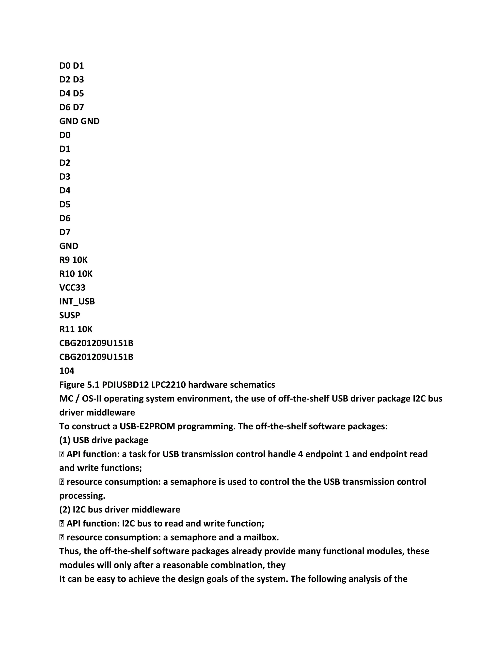


![interrupt nesting depth of
The second line of the Startup.s file read:
IRQ_STACK_LEGTH EQU 9 * 25; each layer nested nine word stack, allowing 25 nesting levels
� USB driver control transmission processing using a semaphore I2C bus driver middleware
uses a
Semaphore and a mailbox, the application of this experiment will use two semaphores, a
total of five events. Because
The definition of the maximum number of events, operating system this os_cfg.h file should
be at least 5:
# Define OS_MAX_EVENTS 5
Statistical tasks � the example and statistical tasks close the (os_cfg.h file):
# Define OS_TASK_STAT_EN 0
Principle analysis in main.c using middleware program, implemented by the I2C bus to read
and write
E2PROM device CAT24WC02.
Disconnect 11. EasyARM2200 development board JP4 jumper JP5 jumper shorted (LPC2210
I2C bus
Pin is connected to CAT24WC02) the the JP6 jumper settings the Bank0-RAM, Bank1-Flash.
12. D12 PACK of to plug into EasyARM2200 development board and the PC with a USB cable
with the D12 PACK even
Pick up.
13. ADS1.2 development environment chosen DebugInExram generate the target, and then
compile the connection works. Select
[Project] -> [Debug], start AXD JTAG emulator debugging.
14 debugger running, PC machines will be prompted to install the new device's USB driver,
USB driver in product
CD, according to a different operating system installed. After installing the USB driver, D12](https://image.slidesharecdn.com/arm1-230111081203-5f490f0b/75/ARM-1-docx-345-2048.jpg)

![===================================================
- 190 -
# Include "I2C.h"
# Define PAGE_SIZE_24C02 16 / / CAT24WC02 page size: 16 bytes
# Define CMD_READ_24C02 0x01 / / Read CAT24WC02 command
# Define CMD_WRITE_24C02 0x02 / / write CAT24WC02 command
OS_STK TaskStartStk [128]; / / operating system starting task stack
OS_STK ReadTaskStk [256]; / / read task stack
OS_STK WriteTaskStk [256]; / / write task stack
OS_EVENT * Write_Sem; / / read tasks ready semaphore
OS_EVENT * Read_Sem; / / write task ready semaphore
2. Configuration PDIUSBD12 interrupt priority and interrupt service routine address. Such as
the program shown in Listing 5.2.
Program Listing 5.2 configuration PDIUSBD12 interrupt
void Init_D12Int (void)
{
VICVectCntl1 = (0x20 | 0x0E); / / EINT0 is channel assigned to IRQ slot 1
VICVectAddr1 = (INT32U) Usb_Handler; / / set EINT0 vector address
VICIntEnable = 1 << 14; / / allow EINT0
}
3. Command from the PC to read and write CAT24WC02 multiple bytes, pointed out that the
command CAT24WC02 the I2C
Bus address, the read or write command, a read or write address, and read and write length.
To do this, define a structure to represent the command.
Such as the program shown in Listing 5.3. And define the structure of a variable I2C.
The command structure of the procedure defined in Listing 5.3 to read and write CAT24WC02
the typedef struct tagCmd / / read and write command structure CAT24WC02
{
INT8U cmd; / / command: 1 - Reading; 2 - write
INT8U addr; / / I2C devices CAT24WC02 address
INT8U offset; / / offset address of the read and write CAT24WC02 storage space
INT16U len; / / read and write length
} I2C_COMMAND;
I2C_COMMAND I2C; / / read and write command structure variables
4. According to the analysis of the experimental principle, following the establishment of the
task construct the system framework shown in Figure 5.2
Section. First, the establishment of the main function main (), the operating system μC / OS-II
multi-task scheduling. Such as the program shown in Listing 5.4.](https://image.slidesharecdn.com/arm1-230111081203-5f490f0b/75/ARM-1-docx-347-2048.jpg)

![===================================================
- 191 -
OSInit (); / / initialize uC / OS-II
OSTaskCreate (TaskStart, (void *) 0, & TaskStartStk [127], 3); / / create a starter task
OSStart (); / / start multi-tasking
}
5. Main function main () create a starting tasks, starting tasks responsible for initializing
hardware (program the manifest 5.5 (1)
~ (4)), to create semaphore control the reading and writing tasks and reading and writing
tasks, before creating the USB control processing tasks. Complete
Into this series, the task as the primary task, constantly waiting for the command from the PC
(program list 5.5 (5)),
To determine for read CAT24WC02 or write CAT24WC02.
5.5 starter task of program listings
void TaskStart (void * pdata)
{
# If OS_CRITICAL_METHOD == 3 / * Allocate storage for CPU status register * /
OS_CPU_SR cpu_sr;
# Endif
INT8U err;
pdata = pdata; / * Prevent compiler warning * /
TargetInit (); / / μC / OS-II timer and related interrupt initialization (1)
I2cInit (30000); / / I2C controller initial (2)
Init_I2CInt (); / / initialize I2C interrupt (3)
Init_D12Int (); / / configure D12 interrupt
err = Init_D12 (); / / PDIUSBD12 initialization (4)
Write_Sem = OSSemCreate (0); / / create two semaphore control the reading and writing
tasks, the initial value of the semaphore is 0
Read_Sem = OSSemCreate (0);
OSTaskCreate (TaskRead, (void *) 0, & ReadTaskStk [255], 1); / / Create a reading task
OSTaskCreate (TaskWrite, (void *) 0, & WriteTaskStk [255], 2); / / create a writing task
if (err == 0) / / initialize the PDIUSBD12 successfully before to create a transmission control
processing tasks
OSTaskCreate (TaskSetup, (void *) 0, & TaskSetupStk [127], 0);
for (; ;) {
err = ReadPort1 (sizeof (I2C_COMMAND) (INT8U *) & I2C, 200); / / wait for commands from
the PC (5)
if (err == OS_NO_ERR) {/ / receive the correct](https://image.slidesharecdn.com/arm1-230111081203-5f490f0b/75/ARM-1-docx-349-2048.jpg)


![===================================================
- 193 -
� writing task in response to the write command, and then began write CAT24WC02 work.
This is done because
Must comply with the rules governing the use of the USB driver package, the rules, see
"Embedded System Software Development
Instance 2.9 USB driver package to use.
� PC machine to receive a response via USB to send the data to be written, LPC2210 I2C bus
driver middleware
These data written to CAT24WC02.
This the � the write CAT24WC02 after, the next crew actually written the number of bytes
sent to the PC, PC machine
Judge whether the writing was successful.
Endpoint 1 sends a write command Director Wushi writing task TaskWrite () Ready
Endpoint 1 receives in response to the writing task: endpoint response to the PC
Data to be written with endpoint 2
Writing tasks: Endpoint 2 receives the data and write
CAT24WC02
Endpoint 1 receives the actual number of bytes written to write tasks: Endpoint 1 sends the
actual number of bytes written
The PC machine EasyARM2200 Development Board
Figure 5.5 writing task framework
Writing tasks such as program shown in Listing 5.7. Program list 5.7 (1) API function to write
CAT24WC02
This function will be described later analysis. The program list 5.7 (2) the length of the data of
the actual write CAT24WC02 via USB mention
For the API function is sent to the PC.
Writing task 5.7 in the program list
void TaskWrite (void * pdata)
{
# If OS_CRITICAL_METHOD == 3 / * Allocate storage for CPU status register * /
OS_CPU_SR cpu_sr;
# Endif
INT8U err, buff [260]; / / send buffer
INT8U ack = 0x02; / / response word
INT16U actlen;
for (; ;) {
OSSemPend (Write_Sem, 0, & err); / / waiting for TaskStart command](https://image.slidesharecdn.com/arm1-230111081203-5f490f0b/75/ARM-1-docx-353-2048.jpg)
![err = WritePort1 (1, & ack, 200); / / response to the PC
if (err == USB_NO_ERR) {/ / answer correctly
err = ReadPort2 (I2C.len, buff, 200); / / receive data to be written
if (err == USB_NO_ERR) {/ / receive the correct
actlen = Write_24WC02 (I2C.addr, I2C.offset, I2C.len, buff); / / execute write (1)
buff [0] = actlen / 256;
buff [1] = actlen% 256;
WritePort1 (2, buff, 200); / / send the actual number of bytes written (2)](https://image.slidesharecdn.com/arm1-230111081203-5f490f0b/75/ARM-1-docx-354-2048.jpg)


![===================================================
- 196 -
{
INT8U pages, nums, i;
INT8U buff [PAGE_SIZE_24C02 + 1]; / / write buffer
INT16U actlen = 0;
pages = len / PAGE_SIZE_24C02; / / CAT24WC02 can only write one, a 16-byte?
nums = len% PAGE_SIZE_24C02; / / not enough integer number of bytes of the page
buff [0] = offset; / / buff [0] offset address for writing
for (i = 0; i <pages; i + +)
{
memcpy (& buff [1], sendbuff, PAGE_SIZE_24C02); / / data to be written will be copied to the
write buffer
actlen the + = I2cWrite (addr, buff, PAGE_SIZE_24C02 + 1) - 1; / / write data and record the
number of bytes written
OSTimeDly (OS_TICKS_PER_SEC / 100 + 1); / / delay time of 10ms so CAT24WC02
/ / Internal write operations
sendbuff + = PAGE_SIZE_24C02;
buff [0] + = PAGE_SIZE_24C02;
}
if (nums> 0)
{/ / Write enough integer page below the number of bytes
memcpy (& buff [1], sendbuff, nums);
actlen + = I2cWrite (addr, buff, nums + 1) - 1;
OSTimeDly (OS_TICKS_PER_SEC / 100 + 1);
}
return actlen; / / return the number of bytes actually written
}
5.1.8 Thinking
Please think about how to use the USB driver package and I2C bus driver middleware
operation
Development board I2C devices EasyARM2200 ZLG7290, use a PC to control the display of the
seven segment display.
5.2 ZLG / CF drive interface function experiments
5.2.1 The purpose of the experiment
� mastered using GPIO pins to read and write and control the timing of the analog ATA
interface;
� the master write ZLG / CF drive interface functions.](https://image.slidesharecdn.com/arm1-230111081203-5f490f0b/75/ARM-1-docx-357-2048.jpg)


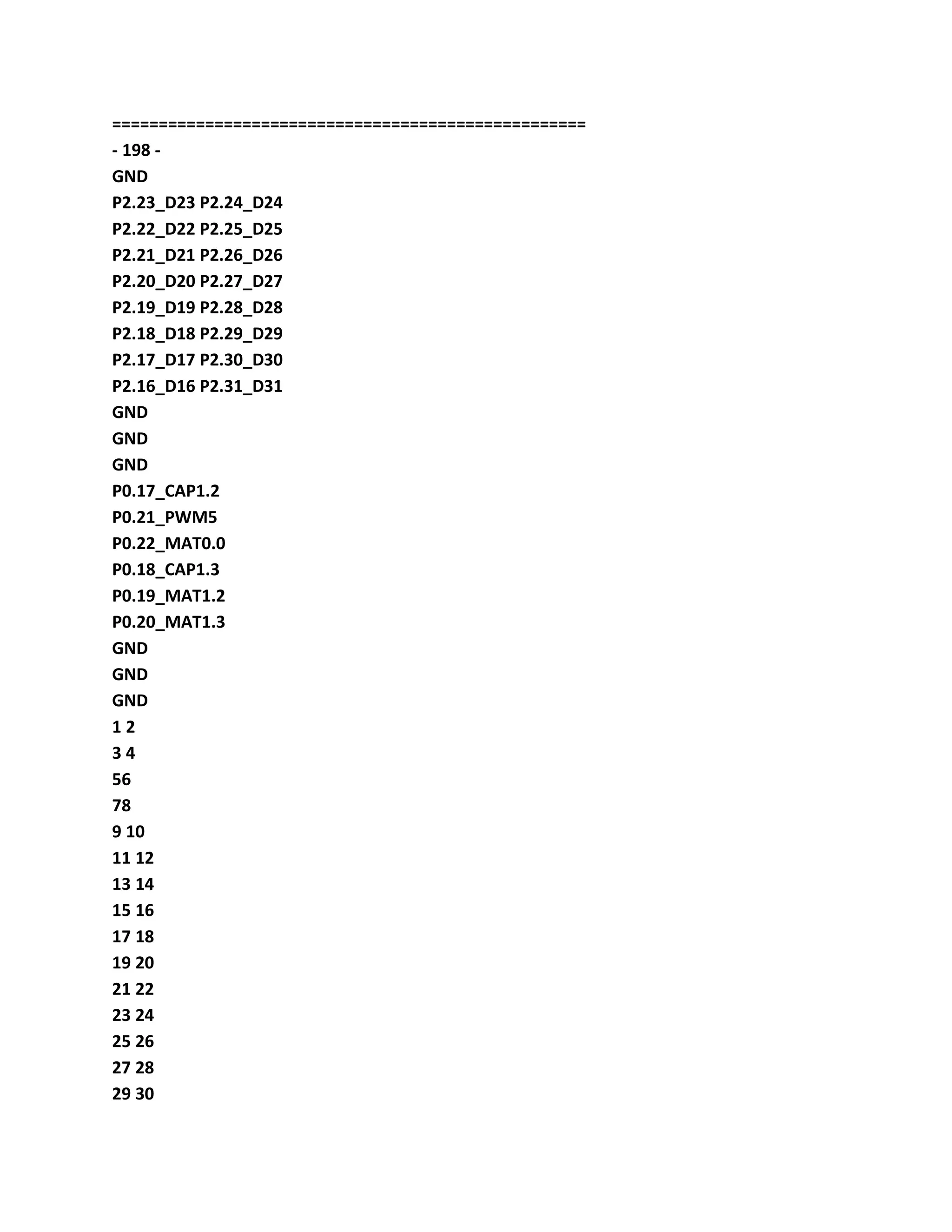
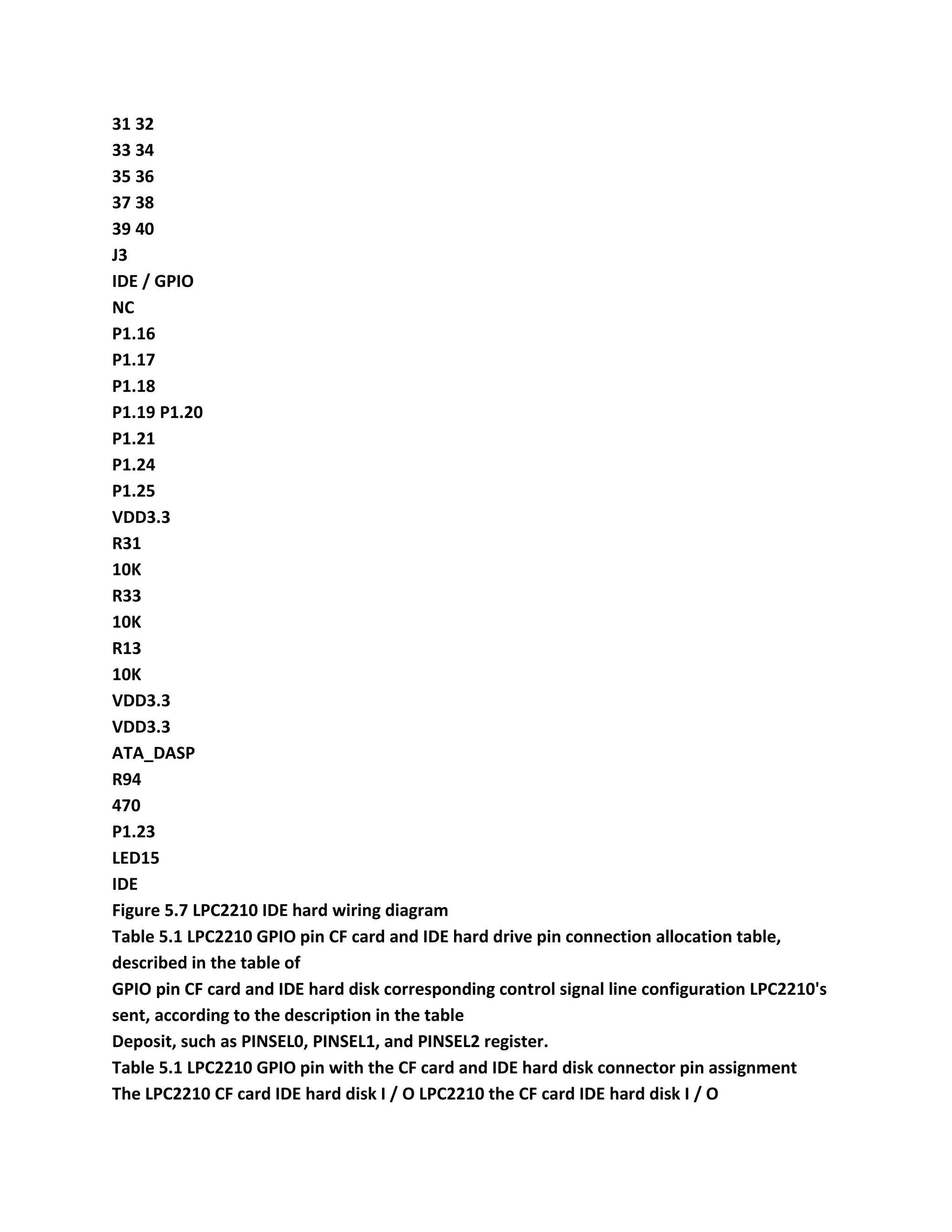


![Write the number (see Note 2)
Data (D15: D00)
-IOCS16
(See Note 3)
IORDY
(See Notes 4,4-1)
IORDY
(See Notes 4,4-2)
IORDY
(See Notes 4,4-3)
Figure 5.8 I / O Timing Diagram
Comment:
Device address-CS0,-CS1 and A [02:00] decision.
2 data from D [15:00] (16) or D [07:00] (8-bit).
3.-IOCS16 PIO modes 0, 1, 2, the other mode, the signal is ignored.
Equipment IORDY low to extend the PIO cycle. -IORD or-IOWR is provided tA time, the master
can be determined cycle is
Whether it is extended. IORDY described in the following three ways:
(1) The device never produce IODRY low level: no wait
(2) The equipment tA before driving IORDY is low, will enable IORDY in tA before set: no wait
(3) equipment in tA before start driving IORDY low: waiting for. IORDY is set again to
complete the cycle. In order to cycle
Generated within the waiting for the signal and set-the IORD, before IORDY is set, tRD signal
device will read data on D15-D00.
5.2.6 Experimental Procedure
Selection of ARM Executable Image for lpc22xx project templates create AtaBus Engineering;](https://image.slidesharecdn.com/arm1-230111081203-5f490f0b/75/ARM-1-docx-369-2048.jpg)
![===================================================
- 200 -
Create SysAta.c, SysAta.H and test.c file and add to the project, and added to the project in
config.h
"# Include" sysata.h ""
Prepared to achieve. SysAta.c file of ZLG / the CF driver interface function code;
4. Preparation of related SysAta.H file, macro definitions and SysAta.c file function
declaration code;
Written in test.c file mina () function code, debugging ZLG / the CF driver interface functions;
6 JP6 jumper EasyARM2200 development board is set to Bank0-RAM, Bank1-Flash;
7 Insert the CF card CF card adapter seat to EasyARM2200 development board connected to
the IDE hard disk (IDE hard drive power
Provided by the PC's power supply);
Selection DebugInExram generate the target, and then compile the connection works.
9 Select [Project] -> [Debug] start AXD JTAG emulator debugging.
10 in the main () function to set a breakpoint, click on the icon of running at full speed, click a
step-by-step debugging single-step operation icon
Procedures to verify that the experimental results:
CF card or IDE hard drive hardware reset;
Read sector count register, observed the the temp1 variable (the mouse to stay in the
variable name), its value should be 0x01;
Read Sector register observe the temp2 variables, its value should be 0x01;
Low reading cylinders, cylinder, device head register values were observed temp3, temp4,
temp5 variables should be as
0x00;
Read the status register and secondary status register, respectively observed temp6, temp7
variables, the value should be 0x50;
Writing a character to the sector register, and then read the sector register observed temp16
variables compare readout and write
Into values.
5.2.7 experimental reference program
1. Related macro definitions and function declarations
Code such as procedures shown in the list of 5.11.
Program list 5.11 macro definitions and function declarations
/ * Where the file: SYSATA.H * /
# Ifndef _SYSATA_H
# Define _SYSATA_H
# Define ATA_DATA 0xffff0000 / * EeayARM2200 and IDE interface directly connected to](https://image.slidesharecdn.com/arm1-230111081203-5f490f0b/75/ARM-1-docx-370-2048.jpg)


![************************************* /
void SYS_PortOut (uint32 reg, uint16 data)
{
OS_ENTER_CRITICAL (); / * disable interrupts * /
Paper IO2DIR = IO2DIR | ATA_DATA; / * set data bus to output * /
IO1CLR = Addr_CS_at_P1; / * address and chip-select signal is low * /
IO1SET = reg; / * Address high bit output, complete address set * /
IO2CLR = ATA_DATA; / * output on the data bus full low * /
IO2SET = data << 16; / * output data high * /
IO0CLR = IDE_WR; / * write signal is low, remains greater than 165nS * /
IO0SET = IDE_WR; / * Write signal pin is set to high [low> 162ns] * /](https://image.slidesharecdn.com/arm1-230111081203-5f490f0b/75/ARM-1-docx-377-2048.jpg)


![===================================================
- 210 -
VICDefVectAddr = (uint32) IRQ_Handler;
VICVectAddr0 = (uint32) Timer0_Handler;
VICVectCntl0 = (0x20 | 0x04);
VICVectAddr1 = (uint32) UART0_Handler; / / allocate UART0 interrupt
vector
VICVectCntl1 = (0x20 | 0x06);
VICIntEnable = (1 << 4) | (1 << 6); / / Enable UART0 interrupt
}
11. Due to the UART0 drive and ZLG / CF drive using a semaphore, so need
os_cfg.h text
Pieces to modify the maximum number of events "OS_MAX_EVENTS", and
at least two additional events:
# Define OS_MAX_EVENTS 2 +2 / * default to two events, at least two
additional events * /
12. Optional DebugInExram generation target, the compiler connection works
(If an error occurs, check the above steps);
13 The the JP6 jumper EasyARM2200 development board is set to Bank0-
RAM, Bank1-Flash;
14. Supporting the serial cable to connect the UART0 port of the PC and the
development board, insert the CF card in the CF adapter seat or
Connection on the IDE interface hard disk (hard drive power provided by the
PC);
15. In ADS 1.2 integrated development environment, select [Project] ->
[Debug] start AXD JTAG imitation
I'm debugging.
16 Click AXD software running at full speed buttons, run the program at full
speed;
17. The run ZLG_CFTest.exe software, selection and development board
connected to the COM port (default COM1) At this time the soft
The pieces will be displayed at the top right of the CF card or IDE hard drive
(as shown in Figure 5.12) If there is no significant
Illustrates the device information, then check the previous step;
Figure 5.12 PC machine software interface](https://image.slidesharecdn.com/arm1-230111081203-5f490f0b/75/ARM-1-docx-389-2048.jpg)

![===================================================
- 212 -
Characters to be written to the CF card or IDE hard disk, and finally click on
"write sector operation" button, then send the number of
Character data region will be written to the specified sector, the status prompt
window will prompt associated;
19 does not change the operation of the previous step, select the "ASCII" in
the "Display Format", and then click on the "read-sector operation"
Button, then receive data area will be displayed before write characters to the
sector, "state prompted window
There will be tips;
20 Click "hard disk motor stop" button, then the hard disk will stop turning
(CF card will enter sleep mode
Type);
21 Click the hard drive motor rotation "button, then the hard disk will begin
to rotate (for CF card will return to the idle mode
Type).
5.3.7 experimental reference program
1. main () function
Code such as procedures shown in the list of 5.22.
List 5.22 main () function
/ *************************************************
******************************************
* Function name: main
* Description: the main function of the c language, it starts multitasking
environment
* Input: None
** Output: None
** Global variables: None
**************************************************
***************************************** /
# Define TASK_STK_SIZE 64
OS_STK TaskStartStk [TASK_STK_SIZE];
int main (void)
{](https://image.slidesharecdn.com/arm1-230111081203-5f490f0b/75/ARM-1-docx-391-2048.jpg)
![OSInit ();
OSTaskCreate (TaskStart, (void *) 0, & TaskStartStk [TASK_STK_SIZE -
1], 0); / / establish TaskStart task
OSStart ();
return 0;
}
2. TaskStart task function
Code such as procedures shown in the list of 5.23.
Procedures Listing 5.23 TaskStart the task
/ *************************************************
******************************************
The ** function names: TaskStart
** Functional Description: μCOS-II first task, usually it initialize the target
board and the establishment of other tasks
* Input: None
** Output: None
** Global variables: None
**************************************************
***************************************** /
uint8 DataBuff [0x10000]; / / save the sector data buffer](https://image.slidesharecdn.com/arm1-230111081203-5f490f0b/75/ARM-1-docx-392-2048.jpg)
![===================================================
- 212 -
# Define DEVICE0 0
void TaskStart (void * pdata)
{
uint16 SectorCount; / / number of sectors
uint32 SectorNumber; / / sector number
uint32 ReceiveData; / / number of bytes of data received
uint16 i;
uint8 RetData, buff [15];
uint8 CommandCode;
pdata = pdata; / * avoid compiler warnings * /
TargetInit (); / * target board initialization * /
for (; ;)
{
err: while ((UART0Getch ()! = 'Z')); / / wait for the PC instruction
for (i = 0; i <15; i + +) buff [i] = UART0Getch ();
if ((buff [0]! = 'L') | | (buff [1]! = 'G') | | (buff [2]! = ':')) goto err; / / not
effective instruction continue to wait
CommandCode = (ASCII_TO_HEX (buff [3]) << 4) | ASCII_TO_HEX (buff
[4]); / / instruction code
SectorNumber = (ASCII_TO_HEX (buff [5]) << 28) | (ASCII_TO_HEX (buff
[6]) << 24) | / / sector number
(ASCII_TO_HEX (buff [7]) << 20) | (ASCII_TO_HEX (buff [8]) << 16) |
(ASCII_TO_HEX (buff [9]) << 12) | (ASCII_TO_HEX (buff [10]) << 8) |
(ASCII_TO_HEX (buff [11]) << 4) | ASCII_TO_HEX (buff [12]);
SectorCount = (ASCII_TO_HEX (buff [13]) << 4) | ASCII_TO_HEX (buff
[14]); / / number of sectors
switch (CommandCode)
{
case 0xE0: / / immediate standby
RetData = ATA_StandbyImmediate (DEVICE0);
break;
case 0xE1: / / immediately idle
RetData = ATA_IdleImmediate (DEVICE0);](https://image.slidesharecdn.com/arm1-230111081203-5f490f0b/75/ARM-1-docx-393-2048.jpg)

![===================================================
- 213 -
OS_ENTER_CRITICAL (); / / disable interrupts
for (i = 0; i <ReceiveData; i + +)
DataBuff [i] = UART0Getch (); / / receiving sector data
OS_EXIT_CRITICAL (); / / open interrupt
RetData = ATA_WriteSector (DEVICE0, (uint16 *) DataBuff, SectorNumber,
SectorCount);
break;
case 0xEC: / / Get device identification information
RetData = ATA_IdentifyDrive (DEVICE0, DataBuff); / / Get Device
identification information
if (RetData)
SendDriveInfo ((PCF_IDENTIFY_DATA) DataBuff); / / transmission device
description information to the PC
break;
default:
RetData = FALSE;
break;
}
RetStateToPC (RetData); / / instruction execution state to return to the PC
}
}
3. ASCII to hexadecimal function
Code such as procedures shown in the list of 5.24.
Program list 5.24 ASCII codes to hexadecimal function
/ *************************************************
***************************
* Name: ASCII_TO_HEX ()
* Function: ASCII code 16 decimal.
**************************************************
************************** /
uint8 ASCII_TO_HEX (uint16 ASCII)
{Uint8 data;
uint8 HEX;](https://image.slidesharecdn.com/arm1-230111081203-5f490f0b/75/ARM-1-docx-395-2048.jpg)


![uint8 RetData2PC [7] = {'S', 'T', 'A', 'T', 'E', ':', 'N'}; / / initialize the return to
the state of the PC
if (RetData)
RetData2PC [6] = 'Y'; / / instruction completes normally
UART0Write (RetData2PC, 7); / / write data to a PC
}
5.3.8 Thinking
ZLG / CF drive ZLG / FS file management system?
5.4 UDP communication experiment
5.4.1 The purpose of the experiment
Experimental control ZLG / IP package the SOCKET API programming
method.](https://image.slidesharecdn.com/arm1-230111081203-5f490f0b/75/ARM-1-docx-398-2048.jpg)


![===================================================
- 217 -
Add in the ADS project window TCPIP file group; then tcpip directory ARP
ARP.C
ETHERNET Ethernet.C, HARDWARE Hardware.c, IP Ip.c, Ping
Icmp.c,
SOCKET zlg_socket.C, TCP TCP.C, UDP UDP.C file is added to the file
group, and finally
The EX1 example TEST.C file disc ZLGIP copy to shiyan , then add to the
ADS
User file group mesh window, shown in Figure 5.15;
The Figure 5.15 shiyan project window
6. In Startup.s files ResetInit subroutine, to modify memory interface Bank3
bus configuration, such as the program cleared
Single 5.27 shown.
Note: The default project template memory interface Bank2, code for the
Bank3 bus configuration is commented out, so
First uncomment (code in front of ";" deleted), you can actually configure
memory interface Bank2 Bank3.
Program list the the 5.27 memory interface Bank3 bus configuration
......
LDR R0, = BCFG3; the set BCFG3 register
LDR R1, = 0x10001460
STR R1, [R0]
7. The EasyARM2200 development panel JP4 short jumper, JP6 jumper set to
Bank0-RAM,
Bank1-Flash, supporting cable Connection EasyARM2200 development board
and PC;
Selection DebugInExram generate target works, compiled connected;
9 Select [Project] -> [Debug] start AXD JTAG emulator debugging, running
at full speed.
Open the Windows operating system in the PC end [Start] -> [run], and then
type "PING IP land
PING was successful, you can see information (IP address for the address-t ",
as shown in Figure 5.16, and then click OK](https://image.slidesharecdn.com/arm1-230111081203-5f490f0b/75/ARM-1-docx-403-2048.jpg)

![===================================================
- 218 -
Figure 5.16 PING command
11. The supporting open the disc in the PC end UDPtest software in the
remote host address bar, type in step 3 set
IP address, remote port number filled in 1025, the local port number filled in
1026 can send data to
EasyARM2200 development board, the results shown in Figure 5.17, the
transmitted data is complete returns, if
Sent to the beginning of a string of "A", it will return five times
"ZLGMCUyhbabcdefghijklmnopqrstuv
wxyz ".
Figure of 5.17 UDPtest software main window
5.4.7 experimental reference program
UDP communication experiment reference program shown in Listing 5.28.
5.28 UDP server program listings
void TaskD (void * pdata)
{
uint8 add [36] = {"ZLGMCUyhbabcdefghijklmnopqrstuvwxyz"}; / / send
data when received "A"
uint8 add1 [10] = {"123456789"}; / / send data error
uint8 rec_buffer [100]; / / send buffer](https://image.slidesharecdn.com/arm1-230111081203-5f490f0b/75/ARM-1-docx-405-2048.jpg)
![===================================================
- 219 -
SOCKET s;
number of uint8 couter_byte = 5; / / repeat send
int rec_coute, send_coute;
uint16 iii;
struct sockaddr servaddr, clientaddr;
OSTimeDly (60);
servaddr.sin_family = 0; / / set the IP address of the client
servaddr.sin_addr [0] = 192;
servaddr.sin_addr [1] = 168;
servaddr.sin_addr [2] = 0;
servaddr.sin_addr [3] = 55;
servaddr.sin_port = 1026; / / set the server port number
s = * socket (0, SOCK_DGRAM, UDP_PROTOCOL); / / establish SOCKET
clientaddr.sin_family = 0;
clientaddr.sin_addr [0] = NetPort [0]. My_Ip [0]; / / set the local IP address
clientaddr.sin_addr [1] = NetPort [0]. My_Ip [1];
clientaddr.sin_addr [2] = NetPort [0]. My_Ip [2];
clientaddr.sin_addr [3] = NetPort [0]. My_Ip [3];
clientaddr.sin_port = 1025; / / set the local listening port number
iii = bind ((SOCKET *) & s, (struct sockaddr *) & clientaddr, sizeof
(clientaddr)) ;/ / bind server address
while (1)
{
rec_coute = recvfrom (s, rec_buffer, 100, 0, (struct sockaddr *) & servaddr, &
iii); / / accept data
if (rec_coute> 0)
{
if (rec_buffer [0] == 'A') / / if the first data is "A"
couter_byte = 5;
else
send_coute = sendto (s, rec_buffer, rec_coute, 0,
(Struct sockaddr *) & servaddr, sizeof (servaddr)) ;/ / accept data return
}](https://image.slidesharecdn.com/arm1-230111081203-5f490f0b/75/ARM-1-docx-406-2048.jpg)


![===================================================
- 223 -
The engineering window Figure 5.20 shiyan the window
6. The EasyARM2200 development panel JP4 short jumper, JP6 jumper set to Bank0-RAM,
Bank1-Flash, with a the supporting cable connection EasyARM2200 development board and a
PC.
7. Generate the target selection DebugInExram, compiled connected engineering;
8 Select [Project] -> [Debug] start AXD JTAG emulator debugging, running at full speed.
Open the Windows operating system in the PC end [Start] -> [Run], and then type "PING IP
address
-T ", shown in Figure 5.21, and then click OK, you can see the PING was successful information
(IP address 3
Step setting the address);
Figure 5.21 PING command
10 Open Microsoft Internet Explorer software in the PC end, set in the address bar, type in
step 3 IP
Address, you can access the page EasyARM2200 development board to run the program, the
results shown in Figure 5.22.](https://image.slidesharecdn.com/arm1-230111081203-5f490f0b/75/ARM-1-docx-413-2048.jpg)
![===================================================
- 224 -
Figure 5.22 WEB server example
5.5.7 experimental reference program
TCP communication experiment reference program shown in Listing 5.29.
Program list 5.29 WEB server task
void TaskE (void * pdata)
{
uint8 Temp = 0;
uint16 TempLength;
int addrlen;
int ei;
uint8 tempdata [400]; / / receive data buffer
SOCKET s;
struct sockaddr servaddr, cliaddr;
OSTimeDly (60);
servaddr.sin_family = 0;
servaddr.sin_addr [0] = NetPort [0]. My_Ip [0]; / / set the IP address of the local SOCKET
servaddr.sin_addr [1] = NetPort [0]. My_Ip [1];
servaddr.sin_addr [2] = NetPort [0]. My_Ip [2];
servaddr.sin_addr [3] = NetPort [0]. My_Ip [3];
servaddr.sin_port = 80; / / set the listener local port
s = * socket (0, 0, 0); / / establish a TCP-based communications SOCKET
ei = bind ((SOCKET *) & s, (struct sockaddr *) & servaddr, sizeof (servaddr)) ;/ / bind local IP
address and listening port
ei = The listen ((SOCKET *) & s, 4); / / listening on the number of connections is four
connections
if (ei! = 4) / / 4 check successfully established connection listener
while (1); / / error handling
while (1)
{
Temp = accept ((SOCKET *) & s, (struct sockaddr *) & cliaddr, & addrlen); / / accept the
client's connection request](https://image.slidesharecdn.com/arm1-230111081203-5f490f0b/75/ARM-1-docx-414-2048.jpg)
![===================================================
- 225 -
if (Temp! = 0xff) / / check if successfully accept connections
{
TempLength = recv (Temp, tempdata, 400, 0); / / read data
if (tempdata [5] == '') / / request a web page?
{
send (Temp, httpweb, 169, 0); / / send a reply
send (Temp, web, 395, 0); / / Send Page
}
else if (tempdata [5] == '1 ') / / request background image?
{
send (Temp, httpgif, 169, 0); / / send a reply
send (Temp, bmp, 442, 0); / / send pictures
}
memset (tempdata, 0,400); / / empty the receive buffer
OSTimeDly (20);
close (Temp); / / Disconnect
}
}
}
5.5.8 Thinking
Writing task based Ethernet to the COM port of the TCP protocol, how to write it?
5.6 GUI Experiment 1
5.6.1 The purpose of the experiment
Experimental understanding of dot matrix graphics LCD module SMG240128A the LPC2210
hardware connections and drive the controlling party
Law and master ZLG / GUI painting function.
5.6.2 The laboratory equipment
� Hardware: PC, a
EasyARM2200 development board set
SMG240128A LCD module one
� software: Windows98/XP/2000 system, ADS 1.2 integrated development environment
ZLG / GUI package
5.6.3 Experimental Content
To use GUI_LoadPic () displays a 40 × 40 icon, and then GUI_Spline () to draw a spline curve,
and then
Use GUI_LineS () to draw a closed polygon and the use GUI_FloodFill () to fill. GUI_PutString ()](https://image.slidesharecdn.com/arm1-230111081203-5f490f0b/75/ARM-1-docx-415-2048.jpg)


![===================================================
- 227 -
/ * Up and down the number of nodes (filled function) * /
# Define DOWNP_N 20
# Define UPP_N 20
/ * The arc function * /
# Define GUI_ArcX_EN 1
/ * Fan function * /
# Define GUI_Pieslice_EN 1
/ * Window manager * /
# Define GUI_WINDOW_EN 0
/ * Icon menu * /
# Define GUI_MenuIco_EN 0
/ * The drop-down menu * /
# Define GUI_MenuDown_EN 0
/ * 5 * 7 font * /
# Define FONT5x7_EN 1
/ * 8 * 8 font * /
# Define FONT8x8_EN 0
/ * 24 * 32 font * /
# Define FONT24x32_EN 0
/ * Chinese character display function * /
# Define GUI_PutHZ_EN 0
/ * Monochrome graphic display function * /
# Define GUI_LoadPic_EN 1
/ * Color conversion * /
# Define CONVERTCOLOR_EN 0
7. Establish C source file lcmdisp.c, the preparation of the experimental procedure, and then
added to the engineering of the user group;
8. In Startup.s files ResetInit subroutine, the to modify memory interface Bank3 bus
configuration (because
The SMG240128A LCD module interface is to use the address space Bank3), shown in Listing
5.32. In order to
The program faster execution, change Bank0 bus configuration for BCFG0, = 0x10000400.
Program list 5.32 the memory interface Bank3 bus configuration
LDR R0, = BCFG0
LDR R1, = 0x10000400
STR R1, [R0]](https://image.slidesharecdn.com/arm1-230111081203-5f490f0b/75/ARM-1-docx-419-2048.jpg)
![===================================================
- 228 -
......
LDR R0, = BCFG3; the set BCFG3 register
LDR R1, = 0x10000CA0
STR R1, [R0]
9. The use DebugInExram generate the target, and then compile the connection works.
10 the JP6 jumper EasyARM2200 development board is set to Bank0-RAM, Bank1-Flash.
11. Of the SMG240128A LCD module insert EasyARM2200 development board J1 connector,
be careful not to put
Wrong direction (1 foot of the LCD module with the corresponding pin 1 of J1). But also to
ensure a reliable connection to prevent contact with not
Benign cause display errors.
12 Select [Project] -> [Debug] start AXD JTAG emulator debugging.
13 program running at full speed, observe the display of the LCD module. (If no, please adjust
EasyARM2200 development board
W3, control the display contrast)
5.6.6 experimental reference program
GUI Experiment 1 reference program shown in Listing 5.33. SMG240128A LCD module driver
files
LCDDRIVE.C, LCDDRIVE.H code, see the product CD-ROM.
Experiment 1 reference program list 5.33 GUI
/ *************************************************
***************************************
* File name: LCMDISP.C
* Function: GUI test and demonstration program.
**************************************************
************************************** /
# Include "config.h"
# Define LCM_LEDCON 0x00400000
/ / Monochrome icon data width x height = 40x40
uint8 const ICO1 [] =
{
0x00, 0x00, 0x00, 0x00, 0x00, 0x00, 0x00, 0x00, 0x00, 0x00, 0x00, 0x00, 0x00, 0x00, 0x00,
0x00,
0x00, 0x00, 0x00, 0x00, 0x00, 0x00, 0xFF, 0x00, 0x00, 0x00, 0x07, 0x00, 0xE0, 0x00, 0x00,
0x18,
0x00, 0x18, 0x00, 0x00, 0x30, 0x00, 0x0C, 0x00, 0x00, 0x40, 0x00, 0x02, 0x00, 0x00, 0x80,](https://image.slidesharecdn.com/arm1-230111081203-5f490f0b/75/ARM-1-docx-420-2048.jpg)

![===================================================
- 229 -
/ / Spline curve 4 endpoint
PointXY log_pin [] = {{80, 30},
{120, 60},
{160, 30},
{200, 60}
};
/ / Closure of the individual vertices of the polygon.
uint32 const poly6 [] = {150,110, 170,80, 180,95, 200,85, 230,110, 150,110};
/ ************************************************* **********************
* Name: main ()
* Function: main program for GUI testing and demonstration.
************************************************** ********************* /
int main (void)
{PINSEL1 = 0x00000000;
IO1DIR = LCM_LEDCON;
IO1SET = LCM_LEDCON;
GUI_Initialize (); / / initialize LCM
GUI_SetColor (1, 0); / / set the foreground and background colors
GUI_LoadPic (30,50, (uint8 *) ICO1, 40, 40); / / display 40 × 40 icon
GUI_Spline (log_pin, 4, 1); / / draw spline curve
GUI_LineS (poly6, 6, 1); / / draw a closed polygon
GUI_FloodFill (160,100, 1); / / filled polygons
GUI_PutString (30,100, "WWW.ZLGMCU.COM"); / / display string
while (1);
return (0);
}
5.6.7 Thinking
ZLG / GUI how to use the API function to display the Chinese characters of the 16 × 16
format?
5.7 GUI Experiment 2
5.7.1 The purpose of the experiment
Experimental understanding of dot matrix graphics LCD module SMG240128A the LPC2210
hardware connections and drive the controlling party
Law, and be able to use ZLG / GUI animation shows.
5.7.2 The laboratory equipment
� Hardware: PC, a](https://image.slidesharecdn.com/arm1-230111081203-5f490f0b/75/ARM-1-docx-422-2048.jpg)


![===================================================
- 232 -
The program faster execution, change Bank0 bus configuration for BCFG0, = 0x10000400.
Program list 5.35 the memory interface Bank3 bus configuration
LDR R0, = BCFG0
LDR R1, = 0x10000400
STR R1, [R0]
......
LDR R0, = BCFG3; the set BCFG3 register
LDR R1, = 0x10000CA0
STR R1, [R0]
9. The use DebugInExram generate the target, and then compile the connection works.
10 the JP6 jumper EasyARM2200 development board is set to Bank0-RAM, Bank1-Flash.
11. Of the SMG240128A LCD module insert EasyARM2200 development board J1 connector,
be careful not to put
Wrong direction (1 foot of the LCD module with the corresponding pin 1 of J1). But also to
ensure a reliable connection to prevent contact with not
Benign cause display errors.
12 Select [Project] -> [Debug] start AXD JTAG emulator debugging.
13 program running at full speed, observe the display of the LCD module. (If no, please adjust
EasyARM2200 development board
W3, control the display contrast)
5.7.7 experimental reference program
GUI experiment reference program shown in Listing 5.36. SMG240128A LCD module driver
files
LCDDRIVE.C, LCDDRIVE.H code, see the product CD-ROM.
Experiment 2 reference program list 5.36 GUI
/ *************************************************
***************************************
* File name: BALL.C
* Function: GUI test and demonstration program.
**************************************************
************************************** /
# Include "config.h"
# Define LCM_LEDCON 0x00400000
/ ************************************************* ***************************
* Name: DelayNS ()
* Function: long software delay](https://image.slidesharecdn.com/arm1-230111081203-5f490f0b/75/ARM-1-docx-428-2048.jpg)


![===================================================
- 238 -
Storage area. Users need to define an array to get enough storage space for the task message
queue, array data type is void
Pointers, such as "void * task1_tmq_buf [30];."
How, then, will be the name of the task queue (pointer) task message queue storage area
linking it? This need to use the built
Li task message queue function TMQ_Create () to achieve, such as "task1_tmq = TMQ_Create
(task1_tmq_buf
30); establish task message queue to be operating before the start uCOS-II.
2 messages
The message structure is defined as shown in the program list 5.37. Among them, wParam
and lParam for additional information, depending on
Type of message, you can have a different role (determined by the user program).
5.37 the definition of the message structure of the program listings
typedef struct tagMSG
{Uint32 message; / / message value
uint32 wParam; / / the message Additional Information 1
uint32 lParam; / / the message Additional Information 2
} MSG;
The type of message (message value) can be defined by the user, defined in the the
experimental the reference program MSG.H file in
As shown in the program list 5.38 several message type, wherein TM is the acronym for the
Task Messag.
The definition of the message type of the program list 5.38
/ / Define the task message, TM abbreviation for Task Message. (Add users in this task
message)
# Define TM_KEY 5762
# Define TM_KEYDOWN 5763
# Define TM_KEYUP 5764
# Define TM_UART0RCV 8974
3 message transmitter
A mission to send a message, pre-defined in a message variable, and then set the parameters
of the message, and then directly use
SendMessage () function can be sent, the reference list of procedures 5.39.
Program list 5.39 messages sent
void TaskUart0 (void * pdata)
{MSG msg_uart0; / / define the message variables msg_uart0](https://image.slidesharecdn.com/arm1-230111081203-5f490f0b/75/ARM-1-docx-440-2048.jpg)


![===================================================
- 240 -
5.8.6 Experimental Procedure
Create a project directory uCOS-II, add μC / OS 2.52 source code and porting code. Also will
be portable PC
The service code Arm_Pc copied into the project directory under uCOS-II.
2 start the ADS 1.2, ARM Executable Image for UCOSII (for lpc22xx) project template to
establish a
Message, a project engineering is stored in the directory uCOS-II.
3. Establish C source file Test.c, the preparation of the experimental procedure, saved to
Message src directory, and then added to the project
The user group.
The task message queue file Msg.c, Msg.h copied to the the Message src directory, then
Msg.c
Add to the engineering of the user group. Config.h file in the project, adding "# include"
MSG.H "".
5 according to the program using the task number of message queues change Os_cfg.h files,
configuration μC / OS-II operating system. Ratio
To use the five task message queue, you can set OS_MAX_EVENTS = 8 OS_MAX_QS = 5
Or greater (but OS_MAX_QS not greater than OS_MAX_EVENTS).
Files in the target group of the project target.c TargetResetInit () function initializes UART0
code
The default initialization for 115200 baud rate can be changed to other baud rate.
7. Use DebugInExram generate the target, and then compile the connection works.
8. EasyARM2200 development board JP9 a short jumper, JP4 jumper off JP6 jumper settings
Bank0-RAM, Bank1-Flash.
9. Use the serial extension cords the EasyARM2200 development boards CZ2 (UART0) and
connected to the PC's COM1.
PC the machine running EasyARM software, set the serial port is COM1, baud rate of 115200,
and then select [set
Set] -> [send data, the open send data window.
10 Select [Project] -> [Debug] start AXD JTAG emulator debugging.
11 run at full speed program. Send on in EasyARM Software hexadecimal number: 5AH, the
receive window of the software
Should receive a to LPC2210 response data 5AH.
12. Shorted / disconnected JP1 P0.14 for low / high, listening buzzer to buzzer.
5.8.7 experimental reference program
System message loop experiment reference program shown in Listing 5.41. The message](https://image.slidesharecdn.com/arm1-230111081203-5f490f0b/75/ARM-1-docx-444-2048.jpg)
![manipulation functions and macros defined in Msg.c text
Pieces and Msg. H (documents, code, see the product CD-ROM).
Program list 5.41 system message loop experiment reference program
/ ************************************************* ***************************
* File name: TEST.C
* Function: Use system message loop mechanism, when key events that send key messages;
When UART0 pick
* Closing event, send an the UART0 receive messages.
* Task 1 message loop control buzzer sounds, receive key messages; receives UART0
* Receive messages, the data received by UART0 return.
************************************************** ************************** /
# Include "config.h"
TMQ * task1_tmq; / / task 1 task message queue (pointer)
/ / GetMessage () waits for a message
void * task1_tmq_buf [30]; / / task 1 task message queue storage area,
/ / TMQ_Create () to establish a task message queue](https://image.slidesharecdn.com/arm1-230111081203-5f490f0b/75/ARM-1-docx-445-2048.jpg)
![===================================================
- 241 -
# Define BEEP (1 << 7)
# Define KEY1 (1 << 14)
# Define TASK_STK_SIZE 64
OS_STK Task1Stk [TASK_STK_SIZE];
OS_STK TaskKeyStk [TASK_STK_SIZE];
OS_STK TaskUart0Stk [TASK_STK_SIZE];
void Task1 (void * pdata);
void TaskUart0 (void * pdata);
void TaskKey (void * pdata);
/ ************************************************* ***************************
* Name: main ()
* Function: main function, start multi-tasking environment.
The * entrance parameters: no
* Export parameters: None
************************************************** ************************** /
int main (void)
{OSInit ();
/ / Task message queue before the system starts to establish
task1_tmq = TMQ_Create (task1_tmq_buf, 30);
OSTaskCreate (Task1, (void *) 0, & Task1Stk [TASK_STK_SIZE - 1], 0);
OSStart ();
return (0);
}
/ ************************************************* ***************************
* Name: UART0_SendByte ()
* Function: send a byte of data to the serial port and waiting to be sent finished.
* Entry parameters: data data to be sent
* Export parameters: None
************************************************** ************************** /
void UART0_SendByte (uint8 data)
{U0THR = data; / / send data
while ((U0LSR & 0x40) == 0); / / wait until the data has been sent
}
/ ************************************************* ***************************
* Name: Task1 ()
* Function: Task 1, receive system messages and processing.](https://image.slidesharecdn.com/arm1-230111081203-5f490f0b/75/ARM-1-docx-446-2048.jpg)
![===================================================
- 242 -
The * entrance Parameters: pdata task initialization parameters
* Export parameters: None
************************************************** ************************** /
void Task1 (void * pdata)
{MSG * pMsg;
pdata = pdata; / / to avoid compiler warnings
TargetInit (); / / target board initialization
PINSEL0 = (PINSEL0 & 0xcffff3ff); / / Pin Select module initialization
IO0DIR | = BEEP; / / Set the buzzer output
IO0SET = BEEP;
IO0DIR & = ~ KEY1; / / set KEY1 input
OSTaskCreate (TaskUart0, (void *) 0, & TaskUart0Stk [TASK_STK_SIZE - 1], 3);
OSTaskCreate (TaskKey, (void *) 0, & TaskKeyStk [TASK_STK_SIZE - 1], 5);
while (1)
{PMsg = GetMessage (task1_tmq);
switch (pMsg-> message)
{Case TM_KEY: / / key message processing
IO0CLR = BEEP;
OSTimeDly (OS_TICKS_PER_SEC / 5);
IO0SET = BEEP;
OSTimeDly (OS_TICKS_PER_SEC / 5);
break;
case TM_UART0RCV: / / UART0 receive the message processing
UART0_SendByte (pMsg-> wParam);
break;
default:
break;
} / / End of switch (pMsg-> message)
}
}
/ ************************************************* ***************************
* Name: UART0_RcvByte ()
* Function: one byte of data read from the UART0 port. If there is no data, direct return.
* Entrance parameters: dat save the read data variable pointer
* Export parameters: returns TRUE indicates that the received data, return FALSE no data
************************************************** ************************** /](https://image.slidesharecdn.com/arm1-230111081203-5f490f0b/75/ARM-1-docx-447-2048.jpg)


![===================================================
- 245 -
Due to the large instantaneous current thermal printer, an output current of at least 3A 5V
regulated power supply
To ensure that the printer is working properly.
Figure 5.24 printer interface connector schematic
5.9.6 Experimental Procedure
Start ADS 1.2, ARM Executable Image for lpc22xx project template to create an engineering
printer.
. To establish C source file Test.c, printer.c and printer.h writing experimental procedures,
and then added to the user of the project
Group.
3 config.h file in the project in the corresponding printer interface the ports definition and
include the header file, such as the program
5.42 shown in the list.
5.42 printer port definition of the program list
......
/ / The following necessary changes
# Define P_DATA_BASE P2 / * data line where the port must be P0, P1, P2 one * /
# Define P_CTR_BASE P2 / * control line where the port must be P0, P1, P2 one * /
# Define P_STATE_BASE P1 / * state line where the port must be P0, P1, P2 one * /
The # define P_DATA_OFFSET 16 / * D0 port where the location, 0 to 24 * /
/ * If P_DATA_BASE for P0 P_DATA_OFFSET 0 * /
/ * D0 in P0.0 D1 located P0.1, and so, following the same * /
# Define P_CTR_OFFSET 24 / * / STROBE port where the location, from 0 to 26 * /
# Define P_STATE_OFFSET 16 / * / ERROR port where the location, from 0 to 27 * /
# Include "printer.h"
Selection DebugInExram generate the target, and then compile the connection works.
5. The EasyARM2200 development board the JP6 jumper settings for Bank0-RAM, Bank1-
Flash.
Connection cable will the printer interface board and EasyARM2200 of development board J3
connection from
EasyARM2200 development board with a 5V power supply, the power supply to the printer
interface board.
7. Connecting cable is used to connect the printer interface board with WH153PA12 miniature
thermal printer, and then use
5V/3A regulated power supply to the printer.
8 Select [Project] -> [Debug] start AXD JTAG emulator debugging.](https://image.slidesharecdn.com/arm1-230111081203-5f490f0b/75/ARM-1-docx-453-2048.jpg)


![===================================================
- 251 -
Send data format: 0xff 0x80 x data 0
0xff: starting byte
0x80: indicates that the LED display
x: the display position 0 to 8, where 8 is a LED lamp.
data: strokes, which are lit, 0 to extinguish.
0: Only avoid 0xff
3. Simulation calendar display
Send data formats: 0xff 0x81 x data 0
0xff: starting byte
0x81: indicates that the LED display
x: position 0 to 14, respectively, corresponding to the year, month, date, day,
hour, minute, needle
data: strokes, which are lit, 0 to extinguish.
0: Only avoid 0xff
4 analog keyboard input
PC sent directly to the serial port the keyboard coding 0 to 19 (byte).
The button the name directory EasyARM.exe file EasyARM.ini file definition,
that is [KeyName]
Changed under the corresponding key names, such as Key10 = A Key11 = B.
5. Simulation DOS character window character color
The program listings A.1 defines the values of constants of the various colors.
The program list A.1 simulation DOS window character color
/ *************************************************
***************************
* File name: COLOR.H
* Features: DOS window character display color definition.
* Description:
**************************************************
************************** /
/ * Foreground color * /
# Define DISP_FGND_BLACK 0x00
# Define DISP_FGND_BLUE 0x01
# Define DISP_FGND_GREEN 0x02](https://image.slidesharecdn.com/arm1-230111081203-5f490f0b/75/ARM-1-docx-460-2048.jpg)


![===================================================
- 252 -
Low, and then reset the system, to enter the ISP the state.
� serial connection is correct
For ISP UART0.
� a serial port resource conflict
Are there other software are using the serial port, or the current serial port is
damaged.
� software settings and operation
ISP software is set up correctly, the correct steps.
B.3 JTAG debug error
JTAG port hardware connection is correct, RTCK pin is connected to a
4.7KΩ pull-down resistor.
When using the JTAG debug process, if there is a system reset (press the RST
key, WDT overflow), the CPU into the
Power down / idle mode, will JTAG debug error. The processing method:
Open the "Options-> Configure AXD in
Target ... ", choose to support the JTAG emulator DLL, and then OK; then
use the" File-> Load Image ... "menu
Load the the debug image file you want to debug (* axf).
LPC2000 chip encrypted the (engineering selection RelInFLASH or
RelInChip goals will LPC2000
Chip encryption LPC2106/2105/2104 and LPC2210/2290 excluded), the JTAG
port can not connect to debug needs
To JTAG connection to use ISP software full chip erase chip debugging.
The B.4 items copied to other directories can not be used
When you copy an existing project to a new directory, open the copied
project, there may be recompiled to link not
Through, this is because the project saved settings or the original directory,
no re-change the file, the linker will be the
Obj files corresponding directory link If you can not find this file error.
Approach: the directory * tdt file deletion, or select the menu [Project] -> In
ADS1.2 [Remove
Object Code ..., to delete obj files in the project "All Targets" button in the
dialog box that pops up.](https://image.slidesharecdn.com/arm1-230111081203-5f490f0b/75/ARM-1-docx-464-2048.jpg)