The document provides an extensive overview of solar cells and photovoltaics, discussing their historical development, operational principles, and the physics of pn junctions. It details the processes of light absorption, electron-hole pair generation, and the factors affecting solar irradiance, including standard spectra for terrestrial applications. Additionally, it covers the mechanisms influencing light behavior as it passes through the atmosphere and their implications for solar energy conversion.


![Just for concept -A p-type material
and n-type material are joined.
Visualize – two tanks containing
water at two different levels are
connected.
Readjusted to single level
Combined energy band diagram
of PN junction - single fermi level
[take it as grounded (reference
voltage is zero)]
EF V = 0
PN junction in equilibrium
Fermi level is constant
Dr. Pius Augustine, SH College, Kochi](https://image.slidesharecdn.com/27piusaugustinesolarcells-200503093546/85/27-pius-augustine-solarcells-21-320.jpg)


![ID = I0 [exp(qVB/nkBT) – 1]
ID –current through the diode IO – reverse saturation current
VB – bias voltage across the diode k-Boltzmann’s constant
n-ideality factor (n = 1 for silicon)
T- temperature in Kelvin
q/kT ≈ 39
I is exponentially proportional to (qVA/kB) and -1
comes from inequilibrium created.
Schockley diode equation or ideal diode equation
Dr. Pius Augustine, SH College, Kochi](https://image.slidesharecdn.com/27piusaugustinesolarcells-200503093546/85/27-pius-augustine-solarcells-35-320.jpg)


![In photovoltaics to quantify the radiation, we usually
use either light intensity or photon flux
Light intensity- also called energy flux or
irradiance, which is energy per area per time,
typically [W/m2] or [mW/cm2]
Photon flux- which is the number of photons
per area per time [cm–2s–1].
Dr. Pius Augustine, SH College, Kochi](https://image.slidesharecdn.com/27piusaugustinesolarcells-200503093546/85/27-pius-augustine-solarcells-42-320.jpg)
![Note:
It is convenient to quantify the photon flux Nph in the
equivalent units of electric current
Jph = q⋅Nph [mA/cm2]
Jph equals the electric current that a cell can deliver if it
converts every photon into a free electron–hole pair.
Dr. Pius Augustine, SH College, Kochi](https://image.slidesharecdn.com/27piusaugustinesolarcells-200503093546/85/27-pius-augustine-solarcells-43-320.jpg)


![ External load is connected
Photocurrent will cause a voltage drop across R ie. V = IR
This voltage will oppose the inbuilt voltage and finally
forward current will start flowing.
ID – forward bias current
ID = ISO [exp (eV/KBT -1)]
ISO - reverse saturation current
Net Current I = ID – Iph.
= ISO [exp (eV/KBT -1)] – Iph
Dr. Pius Augustine, SH College, Kochi](https://image.slidesharecdn.com/27piusaugustinesolarcells-200503093546/85/27-pius-augustine-solarcells-63-320.jpg)
![1. Constant current source which generate current due
to the incident light
2. PN junction which is under forward bias with
forward bias photocurrent ISO [exp (eV/KBT -1)]
3. Currents through above to oppose each other
4. External resistance R
Dr. Pius Augustine, SH College, Kochi](https://image.slidesharecdn.com/27piusaugustinesolarcells-200503093546/85/27-pius-augustine-solarcells-64-320.jpg)


![I-V characteristics of Solar Cell
Dark Current = ISO [exp (eV/KBT -1)]
On shining light
Net Current I = ID – Iph = ISO [exp (eV/KBT -1)] –Iph.
Graph is shifted down (not starting from zero), because of -IPh
Dr. Pius Augustine, SH College, Kochi](https://image.slidesharecdn.com/27piusaugustinesolarcells-200503093546/85/27-pius-augustine-solarcells-67-320.jpg)


![When the graph reaches X – axis, Current is zero
and the voltage is called open circuit voltage (Voc)
I = ID – Iph.
= ISO [exp (eVoc/KBT -1)] –Iph = 0
Rearrange this expression for Voc and
neglecting (-1),
Voc ≈ (KBT/e) ln ( Iph /Iso)
Dr. Pius Augustine, SH College, Kochi](https://image.slidesharecdn.com/27piusaugustinesolarcells-200503093546/85/27-pius-augustine-solarcells-70-320.jpg)

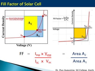
![Power = I * V = ISO [exp (eVoc/KBT -1)] – Iph * V
For Maximum Power dp/dV = 0
On solving, Vm = Voc – (KT/e) ln [1+ (eVm/KBT)]
Recursive relation (Vm on both sides)- solve for Vmax (Vm)
Vm can be substituted for getting Pmax.
Also Im – maximum current at Pmax.
Area within VmIm from I-V graph will give
maximum power
Maximum Power from solar cell?
Dr. Pius Augustine, SH College, Kochi](https://image.slidesharecdn.com/27piusaugustinesolarcells-200503093546/85/27-pius-augustine-solarcells-72-320.jpg)