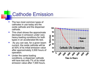
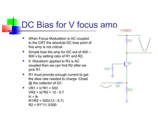
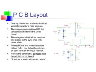
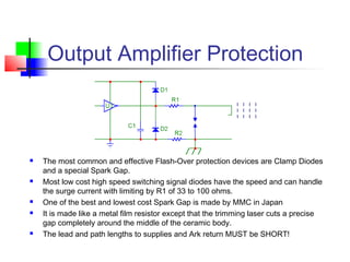
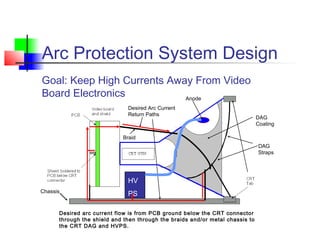
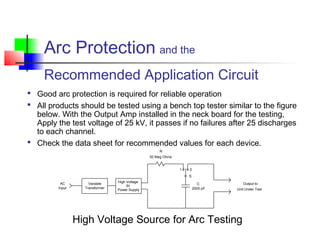
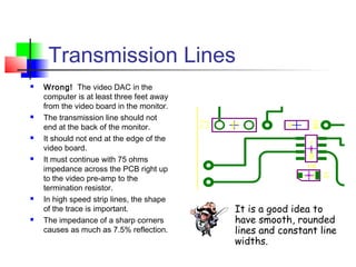
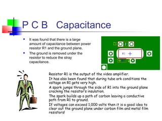
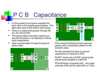
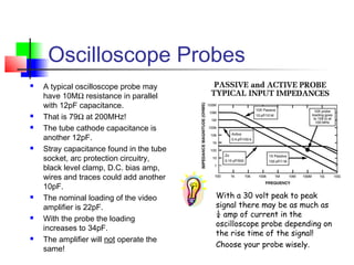
Downloaded 65 times


![Rise Time of Cascaded Stages
It has been said that the whole is the sum of it’s parts. Or at least
the square root of the sum of it’s squares.
For a generator, amp, load, and probe t rise and t fall is given by;
T meas = [T gen2 + T amp2 + T scope2]½
For the amplifier the times are;
T amp = [T meas2 - T gen2 - T scope2]½
4 ~= [72
- 42
- 42
]½
4 ~= [49 - 16 - 16]½](https://image.slidesharecdn.com/a072e578-81bb-45fa-91aa-50a332b093f2-160112213127/85/2-_CRT-Display-Design_A_-41-320.jpg)


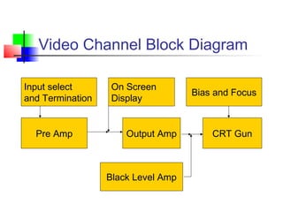

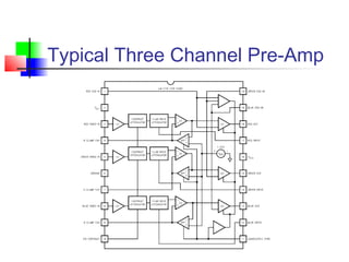
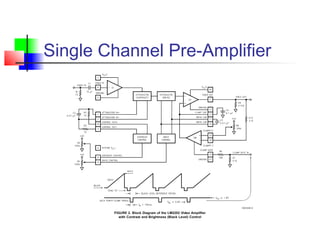
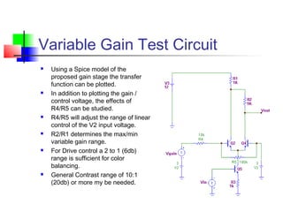
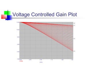
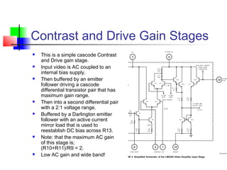
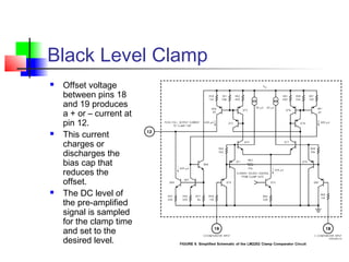
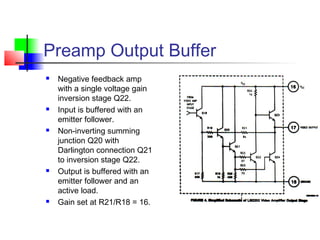
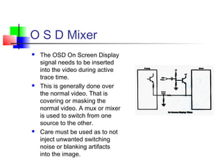
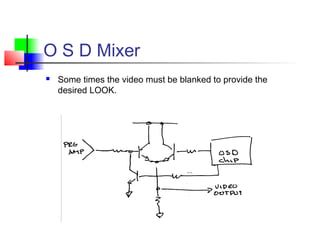


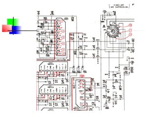


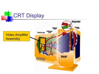
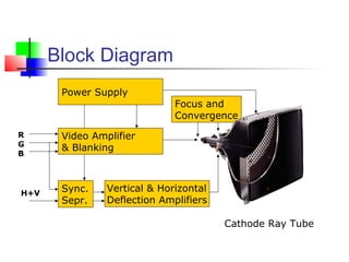
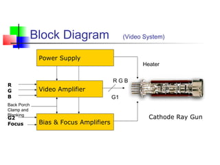
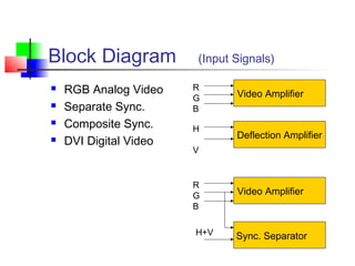
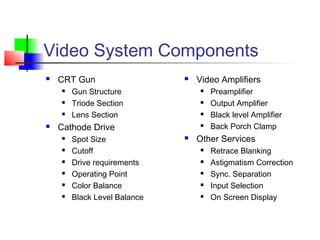
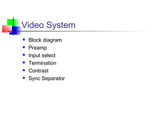
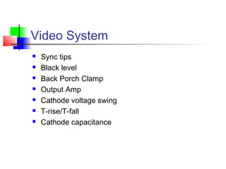
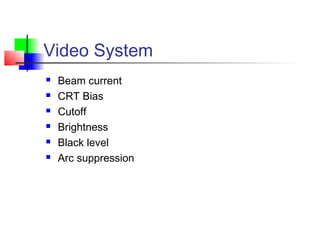
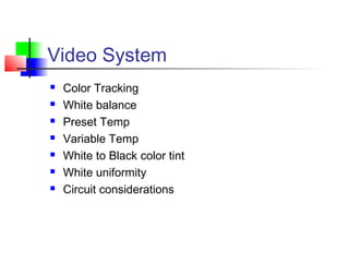
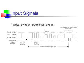
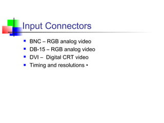
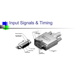
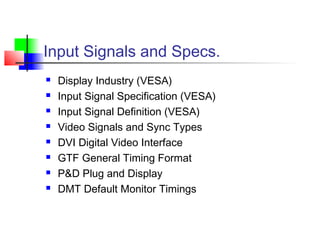
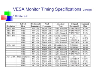
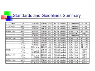
The document provides an overview of CRT display video systems, including: 1) Block diagrams showing the major components of a video system including video amplifiers, sync separator, and focus/convergence circuits. 2) Descriptions of common input signals and timings used in CRT displays. 3) Explanations of key video amplifier sections like pre-amplifiers, output amplifiers, and black level circuits.