
Recommended
More Related Content
What's hot
What's hot (20)
Similar to 137 MHz Low Noise Amplifier Specs
Similar to 137 MHz Low Noise Amplifier Specs (20)
Recently uploaded
Recently uploaded (20)
137 MHz Low Noise Amplifier Specs
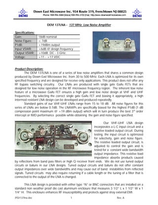
- 1. /PD/137lna.doc 1 Rev. A DEM 137LNA - 137 MHz. Low Noise Amplifier Specifications: Gain: 18dB nominal Noise Figure: <.7dB P1dB: +19dBm output Input VSWR: >6dB @ design frequency Output VSWR: >10dB DC - 3 GHz. Voltage: +11 - +17 VDC Product Description: The DEM 137LNA is one of a series of low noise amplifiers that shares a common design produced by Down East Microwave Inc. from 30 to 500 MHz. Each LNA is optimized for its own specified frequency and are designed for receive only applications. This product does not offer any RF bypass switching circuitry. Our LNAs are produced with single gate GaAs FETs that are designed for low noise operation in the RF microwave frequency region. The inherent low noise feature of a microwave GaAs FET ensures a high gain and low noise design at VHF and UHF frequencies. By selecting the correct single gate GaAs FET and biasing it appropriately, a high intermod resistant LNA design can be developed and produced repeatedly. Standard gains of our VHF-UHF LNAs range from 15 to 18 dB. All noise figures for this series of LNAs are below 0.7dB. The LNAWPs are specifically biased for the highest P1dB (1 dB compression point maximum @ +19 dBm output) which will in turn produce the best 3rd order intercept or IMD performance possible while obtaining the gain and noise figure specified. Our VHF-UHF LNA design incorporates a L-C input circuit and a resistive loaded output circuit. During testing, the input circuit is optimized for selectivity, gain and noise figure. The resistive loaded output circuit, is adjusted to control the gain and is tested for a constant wide bandwidth output impedance. This resistive load impedance absorbs products caused by reflections from band pass filters or high Q receiver front ends. We do not use tuned output circuits or baluns in our LNA designs. Tuned output circuits and baluns do not offer constant output impedances over wide bandwidths and may cause out of band instabilities from reflected signals. Tuned circuits may also require returning if a cable length or the tuning of a filter that is connected to the output of the LNA is changed. This LNA design is provided with either type “N” or BNC connectors that are installed on a standard non weather proof die cast aluminum enclosure that measures 3 1/2” L x 1 1/2” W x 1 1/4” H. This enclosure enhances RF insusceptibility and protects against stray external EMI.
- 2. /PD/137lna.doc 2 Rev. A We do not use folded sheet metal boxes and pop rivets for our enclosures! DC power is applied through a Pi-circuit feed through filter connector, which is a simple solder connection, attenuates all frequencies up through 18 GHz. Coax bias is available on request. This standard design is offered as a PC board parts kit, the VHFLNAK or a complete kit with enclosure and hardware as the VHFLNACK with complete assembly and test instructions. Higher gain models are also available. A similar electrical design is offered in a weather proof enclosure with Type “N” connectors only. Biasing of the weather proof LNA’s can be accomplished through the RF coax if required. Coax biasing is a standard configuration for remote installations such as ATV receivers, scanners, and specialized receive only installations. It is not recommended for repeaters, EME type applications, or standard transceive operating systems. This weather proof enclosure model in not offered as a kit. Specialized custom LNAs with operating frequencies, configurations, gains and noise figures not found on our price list or product descriptions can be designed by DEMI and produced with relatively short delivery times. Please contact us with your specifications and/or requirements. Schematic Diagram of Standard VHF-UHF LNA Design: Output Input + DC INPUT VHFLNAK- PC board Parts Kit VHFLNACK-Contains Parts Kit and Hardware