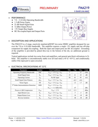
1. PRELIMINARY FMA219
X-BAND LNA MMIC
Phone: +1 408 850-5790 http://www.filtronic.co.uk/semis Revised: 11/22/04
Fax: +1 408 850-5766 Email: sales@filcsi.com
• PERFORMANCE
♦ 7.0 – 11.0 GHz Operating Bandwidth
♦ 1.5 dB Noise Figure
♦ 21 dB Small-Signal Gain
♦ 12 dBm Output Power
♦ +3V Single Bias Supply
♦ DC De-coupled Input and Output Ports
• DESCRIPTION AND APPLICATIONS
The FMA219 is a 2-stage, reactively matched pHEMT low-noise MMIC amplifier designed for use
over the 7.0 to 11.0 GHz bandwidth. The amplifier requires a single +3V supply and one off-chip
component for supply de-coupling. Both the input and output ports are DC de-coupled. Grounding
of the amplifier is provided by plated thru-vias to the bottom of the die, no additional ground is
required.
Typical applications include low-noise front end amplifiers, and general gain block utilizations in X-
band. The amplifier is unconditionally stable over all load states (-45 to +85°C), and conditionally
stable if the input port is open-circuited.
• ELECTRICAL SPECIFICATIONS AT 22°C
Parameter Symbol Test Conditions Min Typ Max Units
Operating Frequency Bandwidth BW VDD = +3 V IDD = IOP 7 11 GHz
Small Signal Gain S21 VDD = +3 V IDD = IOP 19 21 23 dB
Operating Current IOP No RF input 50 65 85 mA
Small Signal Gain Flatness ∆S21 VDD = +3 V IDD = IOP ±0.5 ±0.8
Noise Figure NF VDD = +3 V, IDD = IOP 1.5 1.7 dB
3rd
-Order Intermodulation Distortion IMD VDD = +3 V, IDD = IOP
POUT = +1.5 dBm SCL -47 dBc
Power at 1dB Compression P1dB VDD = +3 V 11.5 12.5 dBm
Input Return Loss S11 VDD = +3 V IDD = IOP -7 -3 dB
Output Return Loss S22 VDD = +3 V IDD = IOP -16 -10 dB
Reverse Isolation S12 VDD = +3 V IDD = IOP -40 -30 dB
2. PRELIMINARY FMA219
X-BAND LNA MMIC
Phone: +1 408 850-5790 http://www.filtronic.co.uk/semis Revised: 11/22/04
Fax: +1 408 850-5766 Email: sales@filcsi.com
• ABSOLUTE MAXIMUM RATINGS1
Parameter Symbol Test Conditions Min Max Units
Supply Voltage VDD For any operating current 6 V
Supply Current IDD For VDD < 5V 100 mA
RF Input Power PIN For standard bias conditions -5 dBm
Storage Temperature TSTG Non-Operating Storage -40 150 ºC
Total Power Dissipation PTOT See De-Rating Note below 600 mW
Gain Compression Comp. Under any bias conditions 5 dB
Simultaneous Combination of Limits2
2 or more Max. Limits 80 %
1
TAmbient = 22°C unless otherwise noted 2
Users should avoid exceeding 80% of 2 or more Limits simultaneously
Notes:
• Operating conditions that exceed the Absolute Maximum Ratings will result in permanent damage to the device.
• Total Power Dissipation defined as: PTOT ≡ (PDC + PIN) – POUT, where:
PDC: DC Bias Power
PIN: RF Input Power
POUT: RF Output Power
• Total Power Dissipation to be de-rated as follows above 22°C:
PTOT= 0.6 - (0.004W/°C) x TCARRIER
where TCARRIER = carrier or heatsink temperature above 22°C
(coefficient of de-rating formula is the Thermal Conductivity)
Example: For a 55°C carrier temperature: PTOT = 0.6 - (0.004 x (55 – 22)) = 0.47W
• For optimum heatsinking eutectic die attach is recommended; conductive epoxy die attach is acceptable with
some degradation in thermal de-rating performance (PTOT = 550mW)
• Note on Thermal Resistivity: The nominal value of 250°C/W is stated for the input stage, which will reach
temperature limits before the output stage. The aggregate MMIC thermal resistivity is approximately 175°C/W.
• HANDLING PRECAUTIONS
To avoid damage to the devices care should be exercised during handling. Proper Electrostatic
Discharge (ESD) precautions should be observed at all stages of storage, handling, assembly, and
testing. These devices should be treated as Class 1A per ESD-STM5.1-1998, Human Body Model.
Further information on ESD control measures can be found in MIL-STD-1686 and MIL-HDBK-263.
• APPLICATIONS NOTES & DESIGN DATA
Applications Notes are available from your local Filtronic Sales Representative or directly from the
factory.
3. PRELIMINARY FMA219
X-BAND LNA MMIC
Phone: +1 408 850-5790 http://www.filtronic.co.uk/semis Revised: 11/22/04
Fax: +1 408 850-5766 Email: sales@filcsi.com
• ASSEMBLY DRAWING
Notes:
• Recommended lead bond technique is thermocompression wedge bonding with 0.001” (25µm) diameter wire. The
bond tool force shall be 35-38 gram. Bonding stage temperature shall be 230-240°C, heated tool (150-160°C) is
recommended. Ultrasonic or thermosonic bonding is not recommended.
• The recommended die attach is conductive epoxy, following the manufacturer’s recommended curing procedure.
• For eutectic die attach the maximum time at 280-300°C is 60 seconds, and should be kept to a minium.
• The supply de-coupling capacitor (150 pF recommended value) should be placed as close to the MMIC as practical.
All information and specifications subject to change without notice.
75µm nominal gap on
each side
250µm Au ribbon
recommended
25µm dia. Au wire (x2) on
input and output ports, less
than 1000µm length each To +VDD
Input and output thin film
substrates with 50Ω microstrip
transmission lines. Substrate
thickness 250µm or thinner is
recommended.
150pF
capacitor
4. PRELIMINARY FMA219
X-BAND LNA MMIC
Phone: +1 408 850-5790 http://www.filtronic.co.uk/semis Revised: 11/22/04
Fax: +1 408 850-5766 Email: sales@filcsi.com
• TYPICAL RF PERFORMANCE (VDD = +3V, IDD = IOP)
• TYPICAL NOISE FIGURE PERFORMANCE
Multiple traces show typical die variation across a 150mm (6 in.) wafer.
Note: Effect of typical bondwire inductance (25 µm dia., 1000 µm length, 2 ea. on input and output
ports) is less than 0.5 dB decrease in S21 (11GHz), and no measurable effect on noise figure.
FMA219BF NOISE FIGURE
0.4
0.5
0.6
0.7
0.8
0.9
1.0
1.1
1.2
1.3
1.4
7 8 9 10 11
Frequency (GHz)
NoiseFigure(dB)
FMA219 FREQUENCY RESPONSE
-20
-16
-12
-8
-4
0
4
8
12
16
20
24
5 6 7 8 9 10 11 12 13 14 15
Frequency [GHz]
SSG,Input/OutputReturnLoss(dB)
S21
S11
S22
5. PRELIMINARY FMA219
X-BAND LNA MMIC
Phone: +1 408 850-5790 http://www.filtronic.co.uk/semis Revised: 11/22/04
Fax: +1 408 850-5766 Email: sales@filcsi.com
• POWER TRANSFER CHARACTERISTIC
• TYPICAL 3RD-ORDER INTERMODULATION PERFORMANCE
FMA219
Equivalent output IP3 performance exceeds 24 dBm, input IP3 is typically ≥ +2 dBm.
FMA219BF POWER TRANSFER CHARACTERISTIC
0.0
2.0
4.0
6.0
8.0
10.0
12.0
14.0
16.0
-23.0 -21.0 -19.0 -17.0 -15.0 -13.0 -11.0 -9.0 -7.0 -5.0 -3.0
Pin (dBm)
OutputPower(dBm)
0.0
0.5
1.0
1.5
2.0
2.5
3.0
3.5
4.0
CompressionPoint,(dB)
Pout@7GHz
Pout@9GHz
Pout@11GHz
Comp@7GHz
Comp@9GHz
Comp@11GHz
IM PRODUCTS vs. INPUT POWER AT 9.0 GHz
1.0
3.0
5.0
7.0
9.0
11.0
-19.0 -17.0 -15.0 -13.0 -11.0 -9.0 -7.0
Input Power (dBm)
Ou
tp
ut
Po
we
r
(d
B
m)
-45.00
-40.00
-35.00
-30.00
-25.00
-20.00
-15.00
IM
Pr
od
uc
ts
(d
Bc
)
Pout Im3, dBc