
Recommended
Recommended
More Related Content
Similar to Crossing the Boundaries: Development Strategies for (P)SoCs
Similar to Crossing the Boundaries: Development Strategies for (P)SoCs (20)
Recently uploaded
Recently uploaded (20)
Crossing the Boundaries: Development Strategies for (P)SoCs
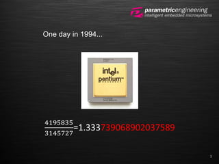
- 1. 1 One day in 1994...
- 2. Development Strategies for (P)SoCs 2 Andreas Koschak Crossing the Boundaries Parametric Engineering GmbH akoschak@parametric.ch Embedded Computing Conference 2013, Winterthur CH
- 3. 3 Short Summary Increased complexity of PSoC and FPGA No Time for Trial and Error FPGA/PSoC based System Development just about to come of age Focus on Verification and Simplicity Systems Engineering Verification Tools Agile SW + FPGA/PSoC Development?
- 4. 4 PSoC Systems Research & Development Technology Consulting OEM Hardware & Software ASIC FPG A Our Field of Activity Focus: Fast Development, Verification and Simplicity, also on System Level, mostly for industrial applications ASSP
- 5. 5 What we see: Difficulty: Hardware and Software partitioning Poor Verification Strategies for FPGA/PSoC Decision-Makers often hesitate to use FPGA/PSoC for more complex tasks
- 6. 6 SoC Microprocessor Core 1 +TCM (Microprocessor Core 2) +TCM RAMROM Periphery Power Supply Generation Analog/RF/ Mixed Signal Circuitry Bus System(s) / Network(s) on Chip Emphasis on Reuse
- 7. 7 FPGAs with integrated Microcontrollers as Hard Macros • Xilinx Zynq • Altera SoC • Microsemi SmartFusion (2) • ARM based Cores (ie. Microsemi ARM Cortex-M1) • NIOS2 • Micro/Picoblaze • LatticeMico • Cadence Xtensa • Many more on Market (8051, LEON, MSP430, PIC, ...) Soft Processors for FPGAs
- 8. 8 The mostly seen (P)SoC Structure Microprocessor Core 1 +TCM RAM ROM Periphery 1 Periphery 2 Periphery 3 Periphery 4 Periphery 5 Bus Bridge Hardware Accelerator
- 9. 9 Microprocessor Core 1 +TCM RAM ROM Periphery 1 Periphery 2 Periphery 3 Periphery 4 Periphery 5 Bus Bridge Hardware Accelerator What happens... Incomplete System Verification Performance Bottleneck
- 10. 10 About Verification... «Verification is a process used to demonstrate that the intent of a design is preserved in its implementation» Janick Bergeron: «Writing Testbenches» Efforts for large ASIC projects:
- 11. 11 Verification Space (Trivial and theoretic) Example Process: 32 Bit Bus Transfer CPU->Periphery (32 Bit Data) 32 Bit Address (2^32 values) 32 Bit Data (2^32 values) Bus Latency Full functional coverage: 2^32 * 2^32 * Latency values
- 12. 12 Microprocessor Core 1 +TCM RAM ROM Periphery 1 Periphery 2 Periphery 3 Periphery 4 Periphery 5 Bus Bridge An alternative Solution Sequencer
- 13. 13 Verification Space -> Alternative Solution (Trivial and theoretic) Example Process: 32 Bit Bus Transfer CPU->Periphery (32 Bit Data) 32 Bit Address (2^32 values) 32 Bit Data (2^32 values) Bus Latency Full functional coverage: 2^32 data values -> Verification possible without BFM (bus functional model!)
- 14. 14 Traditional Verification Approach: Self-Checking Test Bench for UART: BUS Master Model UART TX RXBUS 1. Generate Bus Signals for Write Transfer (Data x) 2. Wait y milliseconds 3. Generate Bus Signals for Command Transfer (Send) 4. Wait z milliseconds 5. Check Signals on TX Pin and compare with expected result What happens if at the same time data is received at the RX port? What happens if the bus is stalled? Create new test cases for each special situation Do you know all of them?
- 15. 15 Contrained Random Approach: BUS Master BFM UART TX RXBUS Random Generator Constraints Assertion Checker Random Generator: Sends random data with random intervals Contraints: Only send data that has to be verified with Assertion Checker: «Check what the system does with the data» UART BFM Constraints Assertion Example: «If the Bus Master sends a data command to address A and later a write command, then the UART must output the byte that has been previously set to address A with a delay of between 0 and 10 microseconds» Result DB You need to be able to repeat exactly the same sequence!
- 16. 16 Our Systems Engineering Approach Requirements DB with Link to Assertions Result DB System Verification FPGA Verification You do not lose time with Requirements Engineering if you do it right! Realtime Functional Coverage Checker Assertion Example: «If the Bus Master sends a data command to address A and later a write command, then the UART must output the byte that has been previously set to address A with a delay of between 0 and 10 microseconds» This is a perfect System Requirement!
- 17. Calculation Servers Calculation Servers 17 A BIG System Requirements DB Result DB Functional Coverage Checker Remote Devices Communication Server Calculation Devices Data Processing Machine Database Server Configuration Server Temporal Assertion Checker Result DB Randomized dynamic Testcase Generator You are here Config DB
- 18. 18 What happens if Requirements Change? 1. Create/Change Requirement(s) in DB 2. Identify new System Level Assertions and link them to Requirements 3. Derive FPGA Assertions 4. Extend Radom Generators if necessary 5. Adapt FPGA Structure 6. Repeat Test Process, first FPGA, then System Test Driven Design on System Level A certain degree of «Agility» is feasible
- 19. 19 Don’t just buy expensive Design Software And try working with it
- 20. 20 Recap: DNFs for FPGA based SoCs 1. D o n ’t l e t R e u s a b i l i t y d i c t a t e y o u r S y s t e m A r c h i t e c t u r e 2. M i n i m i z e D e s i g n S p a c e 3. K e e p F u n c t i o n a l i t y w h e r e i t i s n e e d e d 4. C h e c k T e s t B e n c h e s o f y o u r C o r e s b e f o r e y o u u s e t h e m 5. I d e n t i f y s u i t a b l e V e r i f i c a t i o n E f f o r t (Y o u w i l l m o s t l i k e l y n e v e r b e a b l e t o v e r i f y 100% o f a c o m p l e x S o C j u s t b y s i m u l a t i o n ) 6. A l w a y s m a k e s u r e y o u c a n r e p e a t