8085 stack & machine control instruction
•
0 likes•476 views

machine control & stack related instruction

Recommended
More Related Content
What's hot
What's hot (20)
Similar to 8085 stack & machine control instruction
Similar to 8085 stack & machine control instruction (20)
Recently uploaded
Recently uploaded (20)
8085 stack & machine control instruction
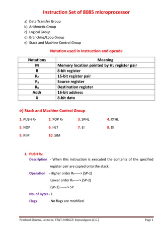
- 1. Prashant Sharma, Lecturer, ET&T, MMGGP, Rajnandgaon (C.G.) Page 1 Instruction Set of 8085 microprocessor a) Data Transfer Group b) Arithmetic Group c) Logical Group d) Branching/Loop Group e) Stack and Machine Control Group Notation used in Instruction and opcode Notations Meaning M Memory location pointed by HL register pair R 8-bit register RP 16-bit register pair RS Source register RD Destination register Addr 16-bit address X 8-bit data e) Stack and Machine Control Group 1. PUSH RP 2. POP RP 3. SPHL 4. XTHL 5. NOP 6. HLT 7. EI 8. DI 9. RIM 10. SIM 1. PUSH RP: Description - When this instruction is executed the contents of the specified register pair are copied onto the stack. Operation - Higher order RP-----> (SP-1) Lower order RP-----> (SP-2) (SP-2) ------> SP No. of Bytes- 1 Flags - No flags are modified.
- 2. Prashant Sharma, Lecturer, ET&T, MMGGP, Rajnandgaon (C.G.) Page 2 Example - PUSH B Before Execution After Execution BC = 1020 H BC = 1020 H SP = 2FFF H SP-1 = 2FFE H = 10H SP-2 = 2FFD H = 20H SP = 2FFD H 2. POP RP: Description - When this instruction is executed the contents of the memory location pointed by the stack pointer register are copied to the low order register of register pair. The stack pointer is incremented by one and the content of that memory location are copied to the higher order register of register pair. Operation - SP-----> Lower order RP (SP+1)-----> Higher order RP (SP+2) ------> SP No. of Bytes- 1 Flags - No flags are modified. Example - POP B Before Execution After Execution BC = 4035 H BC = 1020 H SP = 2FFD H = 20H C = 20H SP+1 = 2FFE H = 10H B = 10H SP+2 = 2FFF H SP = 2FFF H 3. SPHL: Description - Load stack pointer with content of HL register pair. Operation - HL -----> SP No. of Bytes- 1 Flags - No flags are modified. Example - SPHL Before Execution After Execution HL = 2040 H HL = 2040 H SP = 3000 H SP = 2040 H
- 3. Prashant Sharma, Lecturer, ET&T, MMGGP, Rajnandgaon (C.G.) Page 3 4. XTHL: Description - Exchange HL register pair with top of stack. Operation - L <-----> SP H <-----> (SP+1) No. of Bytes- 1 Flags - No flags are modified. Example - XTHL Before Execution After Execution HL = 2040 H HL = 4637H SP = 27FD H = 37H SP = 27FD H = 40H SP + 1 = 27FE H = 46H SP + 1 = 27FE H = 20H 5. NOP (No operation) Description - When this instruction is executed no operation is performed and microprocessor will go for the next instruction after that. Operation - PC + 1 <-----> PC No. of Bytes- 1 Flags - No flags are modified. Example - NOP 6. HLT Description - When this instruction is executed microprocessor complete the instruction and halts any further execution and enters the halt acknowledge machine cycle. Operation - ------ No. of Bytes- 1 Flags - No flags are modified. Example - HLT
- 4. Prashant Sharma, Lecturer, ET&T, MMGGP, Rajnandgaon (C.G.) Page 4 7. EI Description - This instruction is used to enable all maskable interrupts. Operation - ------ No. of Bytes- 1 Flags - No flags are modified. Example - EI 8. DI Description - This instruction is used to disable all maskable interrupts. Operation - ------ No. of Bytes- 1 Flags - No flags are modified. Example - DI 9. SIM(Set Interrupt Mask) Description - This instruction is used to enable or disable RST 7.5, RST 6.5 and RST 5.5 interrupts. It is also used in serial data communication. SIM instruction Format SOD Output Enable Input SOD SDE X R 7.5 MSE M’7.5 M’6.5 M’5.5 Bit No. Pin Description Value Comment D7 SOD Serial output data bit - - D6 SDE Serial data enable 1 Enable serial port 0 Disable serial port D5 X Don’t care - - D4 R 7.5 Reset R 7.5 flip-flop 1 Reset R 7.5 flip-flop 0 No effect on R 7.5 flip-flop Serial output port Interrupt Control Logic
- 5. Prashant Sharma, Lecturer, ET&T, MMGGP, Rajnandgaon (C.G.) Page 5 D3 MSE Mask Set Enable 1 D2 D1 D0 bits are effective 0 D2 D1 D0 bits are ignored D2 M’7.5 Mask RST 7.5 1 Mask or disable RST 7.5 0 Unmask or enable RST 7.5 D1 M’6.5 Mask RST 6.5 1 Mask or disable RST 6.5 0 Unmask or enable RST 6.5 D0 M’5.5 Mask RST 5.5 1 Mask or disable RST 5.5 0 Unmask or enable RST 5.5 Operation - ------ No. of Bytes- 1 Flags - No flags are modified. Example - SIM 10.RIM (Read Interrupt Mask) Description - This instruction is used to check status of all maskable interrupts. It is also used in serial data communication. SIM instruction Format SID SID I 7.5 I 6.5 I 5.5 IE M 7.5 M 6.5 M 5.5 Bit No. Pin Description Value Comment D7 SID Serial input data bit - - D6 I 7.5 RST 7.5 pending 1 RST 7.5 is pending or R 7.5 flip-flop is set 0 RST 7.5 is not active or R 7.5 flip-flop is reset D5 I 6.5 RST 6.5 pending 1 RST 6.5 is pending or RST 6.5 pin is at logic 1 0 RST 6.5 is not active or RST 6.5 pin is at logic 0 Serial input port Interrupt Control Logic
- 6. Prashant Sharma, Lecturer, ET&T, MMGGP, Rajnandgaon (C.G.) Page 6 D4 I 5.5 RST 5.5 pending 1 RST 5.5 is pending or RST 6.5 pin is at logic 1 0 RST 5.5 is not active or RST 6.5 pin is at logic 0 D3 IE Interrupt Enable 1 INTE flip-flop is set or all maskable interrupts are enabled 0 INTE flip-flop is reset or all maskable interrupts are disabled D2 M 7.5 Mask RST 7.5 1 Mask or disable RST 7.5 0 Unmask or enable RST 7.5 D1 M 6.5 Mask RST 6.5 1 Mask or disable RST 6.5 0 Unmask or enable RST 6.5 D0 M 5.5 Mask RST 5.5 1 Mask or disable RST 5.5 0 Unmask or enable RST 5.5 Operation - ------ No. of Bytes- 1 Flags - No flags are modified. Example - RIM