Study of Logic Gates Using Quantum Cellular Automata
pitulgarg_14551008
1. Pitul Garg
M.Tech. Nanotechnology
Ph: 08815219413
Indian Institute of Technology RoorkeeEmail: pitulgarg7@gmail.com
Area of Interest : VLSI, Digital Design.
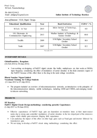
Educational Qualifications Year Board/Institution CGPA* / %
M.Tech. 1st Year 2015
Indian Institute of Technology,
8.0
Roorkee
UG: Electronics &
2013
Madhav Institute of Technology &
80.0
Communication Engineering Science Gwalior
Twelfth 2009
S.M.Higher Secondary School
88.8
Gwalior
Tenth 2007
S.M.Higher Secondary School
82.2
Gwalior
*on a scale of 10
INTERNSHIP DETAILS
GlobalFoundries, Bengaluru
(16-Feb-2016 to 30-June-2016)
I am working on designing of FinFET digital circuits like buffer, multiplexers etc. that works at 30GHz
input frequency considering the effect of modulation of carrier densities in the drain extension region of
the FinFET because of this effect there is the drag in the node voltage waveforms.
Bharat Sanchar Nigam Limited
Vocational Training for College Students
(11-June-2012 to 07-July-2012)
The program included an overview of telecommunications networks, an introduction to the principles of
the telecommunication industry, mobile technologies, including GSM and CDMA, and emerging trends
in telecom networking.
PROJECTS
IIT Roorkee
FinFET Digital Circuit Design methodology considering parasitic Capacitances
(1-July-2015 to 30-June-2016)
Effective capacitances of FinFET logic gate are dependent on transition times at their input-output
nodes due to strong gate controlled modulation of carrier densities in the low doped part of the extension
region which shields gate-extension fringing field capacitance.
I am analyzing the impact of this effect on other logic gates such as Nand gate and inverter followed by
transmission gate.
We are trying to develop a FinFET circuit sizing methodology considering this effect.
2. Madhav Institute of Technology & Science Gwalior
Solar Emergency Light Using DC-AC Inverter
(01-December-2012 to 31-May-2013)
Designing of Charger circuit to charge battery using Solar Energy and designing of another circuit to take
the battery Output so that it is used to illuminate emergency Light source. The designing of circuit is
based on conversion of DC to AC and vice versa.
Electronics Properties and Measurement Techniques of Materials (NTN-605)
Thermal and Electrical Conduction, Modern Theory of solids, Fermi-Dirac statistics, Semiconductors:
temperature dependence of conductivity and mobility, direct indirect semiconductors and dielectric
materials, Band diagram of Metal-oxide-Semiconductor contact.
Nano Scale Devices (EC-587)
CMOS scaling challenges in nanoscale regimes, Devices and technologies for sub 100nm CMOS,
Emerging nanoscale MOSFET.
Physics of Nanomaterial’s (NT-552)
3D and 2D direct lattice, packing fraction, Diffraction from 2D structures, Fermi energy, direct and
indirect semiconductors, lattice matching, hetrostructures and electron states, Carbon Nanostructures.
Nanoscale Modelling and Simulation (NT-511)
Simulation v/s Modelling, Molecular Dynamics, Monte Caro simulation, Course also included some basic
knowledge on MATLAB, Data Structure and Algorithms, Computer programming.
Technology of Nanostructured Fabrication (NT-512)
Moore’s Laws and technology Roadmap–clean rooms Processing Methods: Cleaning, Oxidation,
Lithography, Etching, CVD, Diffusion, Ion implantation, X-ray lithography.
Numerical methods and Statistics (NT-503)
Solutions of equations and eigenvalue problems, Interpolation, Numerical differentiation and numerical
integration, Numerical solution of ordinary differential equations.
Digital VLSI Circuit Design (ECN-573)
CMOS process flow, CMOS Inverter, power consumption, Static characteristics, Combinational logic,
CMOS logic gate sizing considering method of logical effort, Elmore delay model, Sequential logic,
timing issues, clock distribution, jitter, Layout and Design rule, Buffer designing using the concept of
logical effort, Finite State Machines , Mealy and Moore machines.
MOS Device Physics (ECN-572)
PN junction: Current and Capacitance model, Basic of MOS transistors, MOS Capacitor, Non-idealities
in MOS, oxide fixed charges, interfacial charges, physics of MOS, High field effects, Leakages
mechanism, SOI MOSFET, FDSOI and PDSOI, floating body effect.
VLSI physical Design (ECN-591)
Behavioral, structural and physical models, HDL syntax, Verilog/HDL construct, Floor-planning,
placement, Routing, Static timing analysis, Set-up and hold violation, Maximum clock frequency for the
COURSES STUDIED
INDEPENDENT COURSES
3. digital circuits, designing of circuits with no violation or treatment of these violations, clock gating,
VLSI technology (ECN-577)
Crystal growth, Oxidation, Diffusion and ion implantation, Epitaxy and thin film deposition, Etching,
Lithography, Phase shift masks.
SKILLS AND ACHIEVEMENTS
Computer Languages Verilog, Perl, C
Software Packages Cadence, Sentaurus TCAD, Tanner (TSPICE, L-Edit, S-Edit), LT-Spice.
Languages Known English (SRW) , Hindi (SRW)
PERSONAL DETAILS
Father's Name: Rajendra Garg Permanent Address: Dholi Bua Ka Pull,
Date of Birth: March 7, 1992 Bajaria, Lashkar, Gwalior - 474001
Gender: Male Current Address: Manyata Tech park
Contact No: 8815219413 Bengaluru - 560045
REFERENCES
Anand Bulusu Sanjeev Manhas
Associate Professor Associate Professor
Electronics & Communication Dept. Electronics & Communication Dept.
IIT Roorkee IIT Roorkee
anandfec@iitr.ac.in Samanfec@iitr.ac.in
+91-1332-245347 +91-1332-285147
R. Jayaganthan
H.O.D.
Center of Nanotechnology
IIT Roorkee
rjayafmt@iitr.ac.in
+91-1332-285869