
Recommended
More Related Content
What's hot
What's hot (20)
Similar to Nextpcb capabilities 170921
Similar to Nextpcb capabilities 170921 (20)
Recently uploaded
Recently uploaded (20)
Nextpcb capabilities 170921
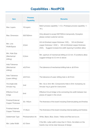
- 1. Capabilities - NextPCB Item Process Capability Remarks Max. Layers 16 Layers Batch process capability: 1-12 L Prototype process capability: 1- 16 L Max. Dimension 500*500mm Only allowed to accept 500*500mm temporarily. Exception please contact customer service Min. Line Width/Space 3/3mil 4/4 mil (finished copper thickness 1OZ),, 5/5 mil (finished copper thickness 1.5OZ ), 6/6 mil (finished copper thickness 2OZ), Suggest increase line width /spacing if condition allow Min. Hole Size (Mechanical drilling) 0.2mm Min. aperture of mechanical drilling is 0.2 mm. If conditions allow suggest enlarge to 0.3 mm or above Hole Tolerance (Mechanical drilling) ±0.07mm The tolerance of mechanical drilling hole is ±0.07mm Hole Tolerance (Laser drilling) ±0.01mm The tolerance of Laser drilling hole is ±0.01mm Via single-side Annular ring 3mil Min. Via is 3mil. Min. Components Hole is 5mil. Increasing via Annular ring is good for overcurrent. Effective Circuit bridge 6mil Effective Circuit bridge is the connecting line width between two pieces of copper in the circuit. Finished External Copper Thickness 35--140um The thickness of the board including External plating and finishes Finished Internal Copper Thickness 17-35um The thickness of the board including Internal plating and finishes Soldermask Type Photosensitive ink White, Black, Blue, Green, Yellow and Red and so on. Min. Letter Width ≥0.15mm If the Min. Letter width is less than 0.15mm, the letters on the boards may not be clear because of design.
- 2. Item Process Capability Remarks Min. Letter Height ≥1mm If the Min. Letter height is less than 1mm, the letters on the boards may not be clear because of design. Letter Aspect Ratio 1:05 The more suitable the Aspect Ratio is, the more convenient for fabrication is. Surface Treatment HASL, HASL Leadfree, ENIG and OSP(for mass production). Board Thickness Range 0.4--3.0mm Conventional board thickness: 0.4/0.6/0.8/1.0/1.2/1.6/2.0 mm, 3.0mm for mass production. Board Thickness Tolerance ±10% The Tolerance of the board thickness. Min. Slot Mill 0.65mm The minimum of the slot mill having copper is 0.65mm, without copper is 0.8mm. Space between Routing and Outline ≥0.25mm(10mil) Min. Plated Slot Width is 0.65mm. Min. Nonplated Routing Slot is 0.8mm. Min. Half-hole 0.6mm Half-hole is a special technology. Array Space (without gap): 0mm space Panel, the space between boards is 0mm. Array Space (without gap) 1.6mm The gap should not less than 1.6mm. Otherwise, it would be difficuit for routing. Peel Strength ≥2.0N/cm Flammability 94V-0 Impedance control Tolerance ±10% Impedance control Bridge ≥5mail Pads Manufacturer Copper Pour Type Hatch Manufacturers adopt Hatch to pour copper. The customers use Pads design PCB please do pay attention to this item.
- 3. Item Process Capability Remarks Draw Slot in Pads Software Use Drill Drawing Layer If there are many non-metallic chemical slots on the boards, please draw on the Drill Drawing Layer Solder-mask Open layer in Protel/dxp software Solder Layer Few engineers mistakenly put this into paste layer. While Huaqiang PCB would not deal with paste layer. Protel /dxp Outline Layer Use Keepout Layer or Machanical Layer Please note: there are only one outline layer allowed in one file, two outline layers is not permitted. Please remove the useless outline layer. That’s to say, just choose either Keepout Layer or Machanical Layer to draw outline. Special Surface Treatment Solder mask is green ink as usual said. Huaqiang PCB can not do S/M Bridge temporarily. Material Type FR - 4, High-frequency plate, Rogers, huaqiang FR4 double-sided PCB boards are made from A-class Jiantao material and the Multilayers boards are from Shengyi Material. Contact GUO Chun HUAQIANG JUFENG NETWORK TECHNOLOGY(HK)LIMITED Factory Add: No.6 Shatou Yumin Rd. Shajing Town, Bao An Dist. Shenzhen 518000 China Skype: uubc_1 www.nextpcb.com/?tid=7 Email: guochun@nextpcb.com