More Related Content Similar to Pic 16 f84 (20) 1. Explore
Su bSmeaitrch
Upload
Login
Signup
Search SlideShare
by gubeybsb Ayty1 kVeAs2bihlbc9yvaey4 aync 1rG otoNeni HraBaiglsulephampu nBrbckeoealr lBrteona C.a.bv...ya. rbVyi cmebunynt eDe eBarnl.akienlc bRoy eB mcaoo..nn.adleegpui byb eym mmkaanzureeel9393
► PPT Presentation ► PowerPoint PPT ► PPT Slides ► PowerPoint Slides
Share Email Embed Like Save
PIC 16F84
Document Transcript
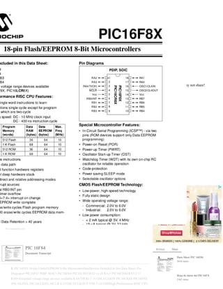
1. PIC16F8X 18-pin Flash/EEPROM 8-Bit MicrocontrollersDevices Included in this Data Sheet: Pin
Diagrams• PIC16F83 PDIP, SOIC• PIC16F84• PIC16CR83 RA2 •1 18 RA1• PIC16CR84 RA3 2 17
RA0• Extended voltage range devices available RA4/T0CKI 3 16 OSC1/CLKIN PIC16CR8X PIC16F8X
(PIC16LF8X, PIC16LCR8X) MCLR 4 15 OSC2/CLKOUT VSS 5 14 VDDHigh Performance RISC CPU
Like this document? Why not share!
Share
Email
Data Sheet PIC 16F84 Data Sheet PIC 16F84 5416 views
Hoja de datos del PIC16FX Hoja de datos del PIC16FX 1362 views
Hoja de datos técnicos del PIC16FX Hoja de datos técnicos del PIC16FX 1382 views
Datasheet Datasheet 1880 views
Test Test 2065 views
35007b 35007b 671 views
16 f877 16 f877 1241 views
PIC Microcontroller PIC Microcontroller 3322 views
Chp4 introduction to the pic microc... Chp4 introduction to the pic microc... 4256 views
Manual pic 18f452 Manual pic 18f452 3927 views
Pic18f458 Pic18f458 748 views
Mpmc Mpmc 2201 views
PIC 16F84
by Alvaro Humberto Cisneros , Working at Revista KANZEN
on Nov 08, 2011
Tweet 0 0
906
views
Follow Like 0 Share
Show more
No comments yet
Related More
Data Sheet PIC 16F84
5416 views
Hoja de datos del PIC16FX
1362 views
2. Features: RB0/INT 6 13 RB7• Only 35 single word instructions to learn RB1 7 12 RB6• All instructions
single cycle except for program RB2 8 11 RB5 branches which are two-cycle RB3 9 10 RB4• Operating
speed: DC - 10 MHz clock input DC - 400 ns instruction cycle Program Data Data Max. Special
Microcontroller Features: Device Memory RAM EEPROM Freq • In-Circuit Serial Programming
(ICSP™) - via two (words) (bytes) (bytes) (MHz) pins (ROM devices support only Data
EEPROMPIC16F83 512 Flash 36 64 10 programming)PIC16F84 1 K Flash 68 64 10 • Power-on Reset
(POR)PIC16CR83 512 ROM 36 64 10 • Power-up Timer (PWRT)PIC16CR84 1 K ROM 68 64 10 •
Oscillator Start-up Timer (OST)• 14-bit wide instructions • Watchdog Timer (WDT) with its own on-chip
RC• 8-bit wide data path oscillator for reliable operation• 15 special function hardware registers • Code-protection•
Eight-level deep hardware stack • Power saving SLEEP mode• Direct, indirect and relative
addressing modes • Selectable oscillator options• Four interrupt sources: CMOS Flash/EEPROM
Technology: - External RB0/INT pin • Low-power, high-speed technology - TMR0 timer overflow • Fully
static design - PORTB<7:4> interrupt on change - Data EEPROM write complete • Wide operating
voltage range:• 1000 erase/write cycles Flash program memory - Commercial: 2.0V to 6.0V - Industrial:
2.0V to 6.0V• 10,000,000 erase/write cycles EEPROM data mem- ory • Low power consumption:•
EEPROM Data Retention > 40 years - < 2 mA typical @ 5V, 4 MHz - 15 μA typical @ 2V, 32
kHzPeripheral Features: - < 1 μA typical standby current @ 2V• 13 I/O pins with individual direction
control• High current sink/source for direct LED drive - 25 mA sink max. per pin - 20 mA source max.
per pin• TMR0: 8-bit timer/counter with 8-bit programmable prescaler© 1998 Microchip Technology Inc.
DS30430C-page 1
2. PIC16F8XTable of Contents1.0 General Description
......................................................................................................................................................................
32.0 PIC16F8X Device Varieties
.......................................................................................................................................................... 53.0
Architectural
Overview..................................................................................................................................................................
74.0 Memory Organization
.................................................................................................................................................................
115.0 I/O
Ports......................................................................................................................................................................................
216.0 Timer0 Module and TMR0
Register............................................................................................................................................ 277.0
Data EEPROM
Memory..............................................................................................................................................................
338.0 Special Features of the CPU
...................................................................................................................................................... 379.0
Instruction Set Summary
............................................................................................................................................................ 5310.0
Development Support
.................................................................................................................................................................
6911.0 Electrical Characteristics for PIC16F83 and
PIC16F84.............................................................................................................. 7312.0 Electrical
Characteristics for PIC16CR83 and
PIC16CR84........................................................................................................ 8513.0 DC & AC
Characteristics
Graphs/Tables.................................................................................................................................... 9714.0
Packaging Information
..............................................................................................................................................................
109Appendix A: Feature Improvements - From PIC16C5X To PIC16F8X
.......................................................................................... 113Appendix B: Code Compatibility - from
PIC16C5X to PIC16F8X.................................................................................................. 113Appendix C:
What’s New In This Data Sheet
................................................................................................................................. 114Appendix D: What’s
Changed In This Data Sheet .........................................................................................................................
114Appendix E: Conversion Considerations - PIC16C84 to PIC16F83/F84 And
PIC16CR83/CR84.................................................. 115Index
Hoja de datos técnicos del PIC16FX
1382 views
Datasheet
1880 views
Test
2065 views
35007b
671 views
16 f877
1241 views
PIC Microcontroller
3322 views
Chp4 introduction to the pic
microcontroller copy
4256 views
Manual pic 18f452
3927 views
Pic18f458
748 views
Mpmc
2201 views
Getting started with pic
microcontrollers
3231 views
Chp7 pic 16 f84 interfacing - copy
1030 views
Pid En Un Pic16 F684
1527 views
Pid En Un Pic16 F684
3526 views
Lab 3 microcontroller
2035 views
PIC -Microcontrollers
16567 views
3. .................................................................................................................................................................................................
117On-Line
Support.................................................................................................................................................................................
119Reader Response
..............................................................................................................................................................................
120PIC16F8X Product Identification System
........................................................................................................................................... 121Sales and
Support..............................................................................................................................................................................
121 To Our Valued Customers We constantly strive to improve the quality of all our products and
documentation. We have spent a great deal of time to ensure that these documents are correct. However,
we realize that we may have missed a few things. If you find any information that is missing or appears in
error, please use the reader response form in the back of this data sheet to inform us. We appreciate your
assistance in making this a better document.DS30430C-page 2 © 1998 Microchip Technology Inc.
3. PIC16F8X1.0 GENERAL DESCRIPTION Table 1-1 lists the features of the PIC16F8X. A simpli- fied
block diagram of the PIC16F8X is shown inThe PIC16F8X is a group in the PIC16CXX family of Figure
3-1.low-cost, high-performance, CMOS, fully-static, 8-bitmicrocontrollers. This group contains the
following The PIC16F8X fits perfectly in applications rangingdevices: from high speed automotive and
appliance motor control to low-power remote sensors, electronic locks,• PIC16F83 security devices and
smart cards. The Flash/EEPROM• PIC16F84 technology makes customization of application•
PIC16CR83 programs (transmitter codes, motor speeds, receiver• PIC16CR84 frequencies, security codes,
etc.) extremely fast andAll PICmicro™ microcontrollers employ an advanced convenient. The small
footprint packages make thisRISC architecture. PIC16F8X devices have enhanced microcontroller series
perfect for all applications withcore features, eight-level deep stack, and multiple space limitations. Low-cost,
low-power, highinternal and external interrupt sources. The separate performance, ease-of-use and
I/O flexibility make theinstruction and data buses of the Harvard architecture PIC16F8X very versatile
even in areas where noallow a 14-bit wide instruction word with a separate microcontroller use has been
considered before8-bit wide data bus. The two stage instruction pipeline (e.g., timer functions; serial
communication; capture,allows all instructions to execute in a single cycle, compare and PWM functions;
and co-processorexcept for program branches (which require two applications).cycles). A total of 35
instructions (reduced instruction The serial in-system programming feature (via twoset) are available.
Additionally, a large register set is pins) offers flexibility of customizing the product afterused to achieve
a very high performance level. complete assembly and testing. This feature can bePIC16F8X
microcontrollers typically achieve a 2:1 code used to serialize a product, store calibration data,
orcompression and up to a 4:1 speed improvement (at 20 program the device with the current firmware
beforeMHz) over other 8-bit microcontrollers in their class. shipping.The PIC16F8X has up to 68 bytes of
RAM, 64 bytes of 1.1 Family and Upward CompatibilityData EEPROM memory, and 13 I/O pins. A
timer/counter is also available. Those users familiar with the PIC16C5X family of microcontrollers will
realize that this is an enhancedThe PIC16CXX family has special features to reduce version of the
PIC16C5X architecture. Please refer toexternal components, thus reducing cost, enhancing Appendix A
for a detailed list of enhancements. Codesystem reliability and reducing power consumption. written for
PIC16C5X devices can be easily ported toThere are four oscillator options, of which the single pin
PIC16F8X devices (Appendix B).RC oscillator provides a low-cost solution, the LPoscillator minimizes
power consumption, XT is a 1.2 Development Supportstandard crystal, and the HS is for High Speed
crystals.The SLEEP (power-down) mode offers power saving. The PIC16CXX family is supported by a
full-featuredThe user can wake the chip from sleep through several macro assembler, a software
simulator, an in-circuitexternal and internal interrupts and resets. emulator, a low-cost development
programmer and aA highly reliable Watchdog Timer with its own on-chip full-featured programmer. A
“C” compiler and fuzzyRC oscillator provides protection against software lock- logic support tools are
also available.up.The devices with Flash program memory allow thesame device package to be used for
prototyping andproduction. In-circuit reprogrammability allows thecode to be updated without the device
being removedfrom the end application. This is useful in thedevelopment of many applications where the
devicemay not be easily accessible, but the prototypes mayrequire code updates. This is also useful for
remoteapplications where the code may need to be updated(such as rate information).© 1998 Microchip
Technology Inc. DS30430C-page 3
4. PIC16F8XTABLE 1-1 PIC16F8X FAMILY OF DEVICES PIC16F83 PIC16CR83 PIC16F84
PIC 18F2550
1297 views
4. PIC16CR84 Maximum Frequency 10 10 10 10Clock of Operation (MHz) Flash Program Memory 512 —
1K — EEPROM Program Memory — — — —Memory ROM Program Memory — 512 — 1K Data
Memory (bytes) 36 36 68 68 Data EEPROM (bytes) 64 64 64 64Peripherals Timer Module(s) TMR0
TMR0 TMR0 TMR0 Interrupt Sources 4 4 4 4 I/O Pins 13 13 13 13Features Voltage Range (Volts) 2.0-
6.0 2.0-6.0 2.0-6.0 2.0-6.0 Packages 18-pin DIP, 18-pin DIP, 18-pin DIP, 18-pin DIP, SOIC SOIC SOIC
SOICAll PICmicro™ Family devices have Power-on Reset, selectable Watchdog Timer, selectable code
protect and high I/O current capa-bility. All PIC16F8X Family devices use serial programming with clock
pin RB6 and data pin RB7.DS30430C-page 4 © 1998 Microchip Technology Inc.
5. PIC16F8X2.0 PIC16F8X DEVICE VARIETIES 2.3 Serialized Quick-Turnaround- Production (SQTP
SM ) DevicesA variety of frequency ranges and packaging optionsare available. Depending on application
and production Microchip offers the unique programming servicerequirements the proper device option
can be selected where a few user-defined locations in each device areusing the information in this section.
When placing programmed with different serial numbers. The serialorders, please use the “PIC16F8X
Product numbers may be random, pseudo-randomIdentification System” at the back of this data sheet to or
sequential.specify the correct part number. Serial programming allows each device to have aThere are four
device “types” as indicated in the device unique number which can serve as an entry-code,number.
password or ID number.1. F, as in PIC16F84. These devices have Flash For information on submitting a
SQTP code, please program memory and operate over the standard contact your Microchip Regional Sales
Office. voltage range.2. LF, as in PIC16LF84. These devices have Flash 2.4 ROM Devices program
memory and operate over an extended voltage range. Some of Microchip’s devices have a corresponding
device where the program memory is a ROM. These3. CR, as in PIC16CR83. These devices have devices
give a cost savings over Microchip’s traditional ROM program memory and operate over the user
programmed devices (EPROM, EEPROM). standard voltage range.4. LCR, as in PIC16LCR84. These
devices have ROM devices (PIC16CR8X) do not allow serialization ROM program memory and operate
over an information in the program memory space. The user extended voltage range. may program this
information into the Data EEPROM.When discussing memory maps and other architectural For
information on submitting a ROM code, pleasefeatures, the use of F and CR also implies the LF and
contact your Microchip Regional Sales Office.LCR versions.2.1 Flash DevicesThese devices are offered
in the lower cost plasticpackage, even though the device can be erased andreprogrammed. This allows the
same device to be usedfor prototype development and pilot programs as wellas production.A further
advantage of the electrically-erasable Flashversion is that it can be erased and reprogrammed in-circuit, or
by device programmers, such as MicrochipsPICSTART® Plus or PRO MATE® II programmers.2.2
Quick-Turnaround-Production (QTP) DevicesMicrochip offers a QTP Programming Service forfactory
production orders. This service is madeavailable for users who choose not to program amedium to high
quantity of units and whose codepatterns have stabilized. The devices have all Flashlocations and
configuration options already pro-grammed by the factory. Certain code and prototypeverification
procedures do apply before productionshipments are available.For information on submitting a QTP code,
pleasecontact your Microchip Regional Sales Office.© 1998 Microchip Technology Inc. DS30430C-page
5
6. PIC16F8XNOTES:DS30430C-page 6 © 1998 Microchip Technology Inc.
7. PIC16F8X3.0 ARCHITECTURAL OVERVIEWThe high performance of the PIC16CXX family can
beattributed to a number of architectural featurescommonly found in RISC microprocessors. To
beginwith, the PIC16CXX uses a Harvard architecture. Thisarchitecture has the program and data
accessed fromseparate memories. So the device has a programmemory bus and a data memory bus. This
improvesbandwidth over traditional von Neumann architecturewhere program and data are fetched from
the samememory (accesses over the same bus). Separatingprogram and data memory further allows
instructions tobe sized differently than the 8-bit wide data word.PIC16CXX opcodes are 14-bits wide,
enabling singleword instructions. The full 14-bit wide program memorybus fetches a 14-bit instruction in
a single cycle. A two-stage pipeline overlaps fetch and execution of instruc-tions (Example 3-1).
Consequently, all instructions exe-cute in a single cycle except for program branches.The PIC16F83 and
PIC16CR83 address 512 x 14 ofprogram memory, and the PIC16F84 and PIC16CR84address 1K x 14
program memory. All program mem-ory is internal.The PIC16CXX can directly or indirectly address
itsregister files or data memory. All special functionregisters including the program counter are mapped
inthe data memory. An orthogonal (symmetrical)instruction set makes it possible to carry out any oper-
5. ation on any register using any addressing mode. Thissymmetrical nature and lack of ‘special
optimalsituations’ make programming with the PIC16CXXsimple yet efficient. In addition, the learning
curve isreduced significantly.© 1998 Microchip Technology Inc. DS30430C-page 7
8. PIC16F8XPIC16CXX devices contain an 8-bit ALU and working The W register is an 8-bit working
register used for ALUregister. The ALU is a general purpose arithmetic unit. operations. It is not an
addressable register.It performs arithmetic and Boolean functions between Depending on the instruction
executed, the ALU maydata in the working register and any register file. affect the values of the Carry
(C), Digit Carry (DC), andThe ALU is 8-bits wide and capable of addition, Zero (Z) bits in the STATUS
register. The C and DC bitssubtraction, shift and logical operations. Unless operate as a borrow and digit
borrow out bit,otherwise mentioned, arithmetic operations are two’s respectively, in subtraction. See the
SUBLW and SUBWFcomplement in nature. In two-operand instructions, instructions for
examples.typically one operand is the working register A simplified block diagram for the PIC16F8X is
shown(W register), and the other operand is a file register or in Figure 3-1, its corresponding pin
description isan immediate constant. In single operand instructions, shown in Table 3-1.the operand is
either the W register or a file register.FIGURE 3-1: PIC16F8X BLOCK DIAGRAM 13 Data Bus 8
Flash/ROM Program Counter EEPROM Data Memory Program Memory PIC16F83/CR83 RAM 512 x 14
File Registers EEPROM 8 Level Stack EEDATA Data Memory PIC16F84/CR84 PIC16F83/CR83 (13-
bit) 36 x 8 64 x 8 1K x 14 PIC16F84/CR84 68 x 8 Program Bus 14 7 RAM Addr EEADR Addr Mux
Instruction reg 5 Direct Addr 7 Indirect TMR0 Addr FSR reg RA4/T0CKI STATUS reg 8 MUX Power-up
Timer I/O Ports 8 Instruction Oscillator Decode & Start-up Timer Control ALU Power-on RA3:RA0
Reset Timing Watchdog RB7:RB1 Timer W reg Generation RB0/INT OSC2/CLKOUT MCLR VDD,
VSS OSC1/CLKINDS30430C-page 8 © 1998 Microchip Technology Inc.
9. PIC16F8XTABLE 3-1 PIC16F8X PINOUT DESCRIPTION DIP SOIC I/O/P Buffer Pin Name
Description No. No. Type TypeOSC1/CLKIN 16 16 I ST/CMOS (3) Oscillator crystal input/external
clock source input.OSC2/CLKOUT 15 15 O — Oscillator crystal output. Connects to crystal or resonator
in crystal oscillator mode. In RC mode, OSC2 pin outputs CLKOUT which has 1/4 the frequency of
OSC1, and denotes the instruction cycle rate.MCLR 4 4 I/P ST Master clear (reset) input/programming
voltage input. This pin is an active low reset to the device. PORTA is a bi-directional I/O port.RA0 17 17
I/O TTLRA1 18 18 I/O TTLRA2 1 1 I/O TTLRA3 2 2 I/O TTLRA4/T0CKI 3 3 I/O ST Can also be
selected to be the clock input to the TMR0 timer/ counter. Output is open drain type. PORTB is a bi-directional
I/O port. PORTB can be software pro- grammed for internal weak pull-up on all
inputs.RB0/INT 6 6 I/O TTL/ST (1) RB0/INT can also be selected as an external interrupt pin.RB1 7 7
I/O TTLRB2 8 8 I/O TTLRB3 9 9 I/O TTLRB4 10 10 I/O TTL Interrupt on change pin.RB5 11 11 I/O
TTL Interrupt on change pin.RB6 12 12 I/O TTL/ST (2) Interrupt on change pin. Serial programming
clock.RB7 13 13 I/O TTL/ST (2) Interrupt on change pin. Serial programming data.VSS 5 5 P — Ground
reference for logic and I/O pins.VDD 14 14 P — Positive supply for logic and I/O pins.Legend: I= input
O = output I/O = Input/Output P = power — = Not used TTL = TTL input ST = Schmitt Trigger
inputNote 1: This buffer is a Schmitt Trigger input when configured as the external interrupt. 2: This
buffer is a Schmitt Trigger input when used in serial programming mode. 3: This buffer is a Schmitt
Trigger input when configured in RC oscillator mode and a CMOS input otherwise.© 1998 Microchip
Technology Inc. DS30430C-page 9
10. PIC16F8X3.1 Clocking Scheme/Instruction Cycle 3.2 Instruction Flow/PipeliningThe clock input
(from OSC1) is internally divided by An “Instruction Cycle” consists of four Q cycles (Q1,four to
generate four non-overlapping quadrature Q2, Q3 and Q4). The instruction fetch and execute areclocks
namely Q1, Q2, Q3 and Q4. Internally, the pipelined such that fetch takes one instruction cycleprogram
counter (PC) is incremented every Q1, the while decode and execute takes another instructioninstruction
is fetched from the program memory and cycle. However, due to the pipelining, each instructionlatched
into the instruction register in Q4. The effectively executes in one cycle. If an instructioninstruction is
decoded and executed during the causes the program counter to change (e.g., GOTO)following Q1
through Q4. The clocks and instruction then two cycles are required to complete the instructionexecution
flow is shown in Figure 3-2. (Example 3-1). A fetch cycle begins with the Program Counter (PC)
incrementing in Q1. In the execution cycle, the fetched instruction is latched into the “Instruction
Register” in cycle Q1. This instruction is then decoded and executed during the Q2, Q3, and Q4 cycles.
Data memory is read during Q2 (operand read) and written during Q4 (destination write).FIGURE 3-2:
6. CLOCK/INSTRUCTION CYCLE Q1 Q2 Q3 Q4 Q1 Q2 Q3 Q4 Q1 Q2 Q3 Q4 OSC1 Q1 Q2 Internal
phase Q3 clock Q4 PC PC PC+1 PC+2 OSC2/CLKOUT (RC mode) Fetch INST (PC) Execute INST (PC-
1) Fetch INST (PC+1) Execute INST (PC) Fetch INST (PC+2) Execute INST (PC+1)EXAMPLE 3-1:
INSTRUCTION PIPELINE FLOW 1. MOVLW 55h Fetch 1 Execute 1 2. MOVWF PORTB Fetch 2
Execute 2 3. CALL SUB_1 Fetch 3 Execute 3 4. BSF PORTA, BIT3 Fetch 4 Flush Fetch SUB_1 Execute
SUB_1 All instructions are single cycle, except for any program branches. These take two cycles since the
fetch instruction is “flushed” from the pipeline while the new instruction is being fetched and then
executed.DS30430C-page 10 © 1998 Microchip Technology Inc.
11. PIC16F8X4.0 MEMORY ORGANIZATION FIGURE 4-1: PROGRAM MEMORY MAP AND
STACK - PIC16F83/CR83There are two memory blocks in the PIC16F8X. Theseare the program memory
and the data memory. Each PC<12:0>block has its own bus, so that access to each block can CALL,
RETURN 13occur during the same oscillator cycle. RETFIE, RETLWThe data memory can further be
broken down into the Stack Level 1 • •general purpose RAM and the Special Function •Registers (SFRs).
The operation of the SFRs that Stack Level 8control the “core” are described here. The SFRs usedto
control the peripheral modules are described in the Reset Vector 0000hsection discussing each individual
peripheral module. Peripheral Interrupt Vector 0004h User MemoryThe data memory area also contains
the data SpaceEEPROM memory. This memory is not directly mappedinto the data memory, but is
indirectly mapped. That is,an indirect address pointer specifies the address of thedata EEPROM memory
to read/write. The 64 bytes ofdata EEPROM memory have the address range 1FFh0h-3Fh. More details
on the EEPROM memory can befound in Section 7.0.4.1 Program Memory OrganizationThe PIC16FXX
has a 13-bit program counter capable 1FFFhof addressing an 8K x 14 program memory space. Forthe
PIC16F83 and PIC16CR83, the first 512 x 14(0000h-01FFh) are physically implemented FIGURE 4-2:
PROGRAM MEMORY MAP(Figure 4-1). For the PIC16F84 and PIC16CR84, the AND STACK -
PIC16F84/CR84first 1K x 14 (0000h-03FFh) are physically imple-mented (Figure 4-2). Accessing a
location above the PC<12:0>physically implemented address will cause a wrap- CALL, RETURN
13around. For example, for the PIC16F84 locations 20h, RETFIE, RETLW420h, 820h, C20h, 1020h,
1420h, 1820h, and 1C20h Stack Level 1 •will be the same instruction. • •The reset vector is at 0000h and
the interrupt vector is Stack Level 8at 0004h. Reset Vector 0000h Peripheral Interrupt Vector 0004h User
Memory Space 3FFh 1FFFh© 1998 Microchip Technology Inc. DS30430C-page 11
12. PIC16F8X4.2 Data Memory Organization 4.2.1 GENERAL PURPOSE REGISTER FILEThe data
memory is partitioned into two areas. The first All devices have some amount of General Purposeis the
Special Function Registers (SFR) area, while the Register (GPR) area. Each GPR is 8 bits wide and
issecond is the General Purpose Registers (GPR) area. accessed either directly or indirectly through the
FSRThe SFRs control the operation of the device. (Section 4.5).Portions of data memory are banked. This
is for both The GPR addresses in bank 1 are mapped tothe SFR area and the GPR area. The GPR area is
addresses in bank 0. As an example, addressing loca-banked to allow greater than 116 bytes of general
tion 0Ch or 8Ch will access the same GPR.purpose RAM. The banked areas of the SFR are for
theregisters that control the peripheral functions. Banking 4.2.2 SPECIAL FUNCTION
REGISTERSrequires the use of control bits for bank selection. The Special Function Registers (Figure 4-
1, Figure 4-2These control bits are located in the STATUS Register. and Table 4-1) are used by the CPU
and PeripheralFigure 4-1 and Figure 4-2 show the data memory map functions to control the device
operation. Theseorganization. registers are static RAM.Instructions MOVWF and MOVF can move values
from The special function registers can be classified into twothe W register to any location in the register
file (“F”), sets, core and peripheral. Those associated with theand vice-versa. core functions are described
in this section. ThoseThe entire data memory can be accessed either related to the operation of the
peripheral features aredirectly using the absolute address of each register file described in the section for
that specific feature.or indirectly through the File Select Register (FSR)(Section 4.5). Indirect addressing
uses the presentvalue of the RP1:RP0 bits for access into the bankedareas of data memory.Data memory is
partitioned into two banks whichcontain the general purpose registers and the specialfunction registers.
Bank 0 is selected by clearing theRP0 bit (STATUS<5>). Setting the RP0 bit selects Bank1. Each Bank
extends up to 7Fh (128 bytes). The firsttwelve locations of each Bank are reserved for theSpecial Function
Registers. The remainder are Gen-eral Purpose Registers implemented as static RAM.DS30430C-page 12
© 1998 Microchip Technology Inc.
13. PIC16F8XFIGURE 4-1: REGISTER FILE MAP - FIGURE 4-2: REGISTER FILE MAP -
7. PIC16F83/CR83 PIC16F84/CR84 File Address File Address File Address File Address (1) (1) 00h
Indirect addr. Indirect addr. 80h 00h Indirect addr.(1) Indirect addr.(1) 80h 01h TMR0 OPTION 81h 01h
TMR0 OPTION 81h 02h PCL PCL 82h 02h PCL PCL 82h 03h STATUS STATUS 83h 03h STATUS
STATUS 83h 04h FSR FSR 84h 04h FSR FSR 84h 05h PORTA TRISA 85h 05h PORTA TRISA 85h
06h PORTB TRISB 86h 06h PORTB TRISB 86h 07h 87h 07h 87h 08h EEDATA EECON1 88h 08h
EEDATA EECON1 88h 09h EEADR EECON2(1) 89h 09h EEADR EECON2(1) 89h 0Ah PCLATH
PCLATH 8Ah 0Ah PCLATH PCLATH 8Ah 0Bh INTCON INTCON 8Bh 0Bh INTCON INTCON 8Bh
0Ch 8Ch 0Ch 8Ch 36 General Mapped Purpose (accesses) registers in Bank 0 68 (SRAM) General
Mapped Purpose (accesses) 2Fh AFh registers in Bank 0 (SRAM) 30h B0h 4Fh CFh 50h D0h 7Fh FFh
7Fh FFh Bank 0 Bank 1 Bank 0 Bank 1 Unimplemented data memory location; read as ’0’.
Unimplemented data memory location; read as ’0’. Note 1: Not a physical register. Note 1: Not a physical
register.© 1998 Microchip Technology Inc. DS30430C-page 13
14. PIC16F8XTABLE 4-1 REGISTER FILE SUMMARY Value on Value on allAddress Name Bit 7 Bit
6 Bit 5 Bit 4 Bit 3 Bit 2 Bit 1 Bit 0 Power-on other resets Reset (Note3) Bank 000h INDF Uses contents of
FSR to address data memory (not a physical register) ---- ---- ---- ----01h TMR0 8-bit real-time
clock/counter xxxx xxxx uuuu uuuu02h PCL Low order 8 bits of the Program Counter (PC) 0000 0000
0000 0000 (2) TO03h STATUS IRP RP1 RP0 PD Z DC C 0001 1xxx 000q quuu04h FSR Indirect data
memory address pointer 0 xxxx xxxx uuuu uuuu05h PORTA — — — RA4/T0CKI RA3 RA2 RA1 RA0 -
--x xxxx ---u uuuu06h PORTB RB7 RB6 RB5 RB4 RB3 RB2 RB1 RB0/INT xxxx xxxx uuuu uuuu07h
Unimplemented location, read as 0 ---- ---- ---- ----08h EEDATA EEPROM data register xxxx xxxx uuuu
uuuu09h EEADR EEPROM address register xxxx xxxx uuuu uuuu0Ah PCLATH — — — Write buffer
for upper 5 bits of the PC (1) ---0 0000 ---0 00000Bh INTCON GIE EEIE T0IE INTE RBIE T0IF INTF
RBIF 0000 000x 0000 000uBank 180h INDF Uses contents of FSR to address data memory (not a
physical register) ---- ---- ---- ---- OPTION_ 1111 1111 1111 111181h RBPU INTEDG T0CS T0SE PSA
PS2 PS1 PS0 REG82h PCL Low order 8 bits of Program Counter (PC) 0000 0000 0000 000083h
STATUS (2) IRP RP1 RP0 TO PD Z DC C 0001 1xxx 000q quuu84h FSR Indirect data memory address
pointer 0 xxxx xxxx uuuu uuuu85h TRISA — — — PORTA data direction register ---1 1111 ---1
111186h TRISB PORTB data direction register 1111 1111 1111 111187h Unimplemented location, read
as 0 ---- ---- ---- ----88h EECON1 — — — EEIF WRERR WREN WR RD ---0 x000 ---0 q00089h
EECON2 EEPROM control register 2 (not a physical register) ---- ---- ---- ----0Ah PCLATH — — —
Write buffer for upper 5 bits of the PC (1) ---0 0000 ---0 00000Bh INTCON GIE EEIE T0IE INTE RBIE
T0IF INTF RBIF 0000 000x 0000 000uLegend: x = unknown, u = unchanged. - = unimplemented read as
’0’, q = value depends on condition.Note 1: The upper byte of the program counter is not directly
accessible. PCLATH is a slave register for PC<12:8>. The contents of PCLATH can be transferred to the
upper byte of the program counter, but the contents of PC<12:8> is never transferred to PCLATH. 2: The
TO and PD status bits in the STATUS register are not affected by a MCLR reset. 3: Other (non power-up)
resets include: external reset through MCLR and the Watchdog Timer Reset.DS30430C-page 14 © 1998
Microchip Technology Inc.
15. PIC16F8X4.2.2.1 STATUS REGISTER Only the BCF, BSF, SWAPF and MOVWF instructions
should be used to alter the STATUS register (Table 9-2)The STATUS register contains the arithmetic
status of because these instructions do not affect any status bit.the ALU, the RESET status and the bank
select bit fordata memory. Note 1: The IRP and RP1 bits (STATUS<7:6>) are not used by the PIC16F8X
and should beAs with any register, the STATUS register can be the programmed as cleared. Use of these
bitsdestination for any instruction. If the STATUS register is as general purpose R/W bits is NOTthe
destination for an instruction that affects the Z, DC recommended, since this may affector C bits, then the
write to these three bits is disabled. upward compatibility with future products.These bits are set or cleared
according to device logic.Furthermore, the TO and PD bits are not writable. Note 2: The C and DC bits
operate as a borrowTherefore, the result of an instruction with the STATUS and digit borrow out bit,
respectively, inregister as destination may be different than intended. subtraction. See the SUBLW and
SUBWF instructions for examples.For example, CLRF STATUS will clear the upper-threebits and set the
Z bit. This leaves the STATUS register Note 3: When the STATUS register is theas 000u u1uu (where u =
unchanged). destination for an instruction that affects the Z, DC or C bits, then the write to these three bits
is disabled. The specified bit(s) will be updated according to device logicFIGURE 4-1: STATUS
REGISTER (ADDRESS 03h, 83h) R/W-0 R/W-0 R/W-0 R-1 R-1 R/W-x R/W-x R/W-x IRP RP1 RP0 TO
PD Z DC C R = Readable bit bit7 bit0 W = Writable bit U = Unimplemented bit, read as ‘0’ - n = Value at
8. POR reset bit 7: IRP: Register Bank Select bit (used for indirect addressing) 0 = Bank 0, 1 (00h - FFh) 1 =
Bank 2, 3 (100h - 1FFh) The IRP bit is not used by the PIC16F8X. IRP should be maintained clear. bit 6-
5: RP1:RP0: Register Bank Select bits (used for direct addressing) 00 = Bank 0 (00h - 7Fh) 01 = Bank 1
(80h - FFh) 10 = Bank 2 (100h - 17Fh) 11 = Bank 3 (180h - 1FFh) Each bank is 128 bytes. Only bit RP0
is used by the PIC16F8X. RP1 should be maintained clear. bit 4: TO: Time-out bit 1 = After power-up,
CLRWDT instruction, or SLEEP instruction 0 = A WDT time-out occurred bit 3: PD: Power-down bit 1 =
After power-up or by the CLRWDT instruction 0 = By execution of the SLEEP instruction bit 2: Z: Zero
bit 1 = The result of an arithmetic or logic operation is zero 0 = The result of an arithmetic or logic
operation is not zero bit 1: DC: Digit carry/borrow bit (for ADDWF and ADDLW instructions) (For
borrow the polarity is reversed) 1 = A carry-out from the 4th low order bit of the result occurred 0 = No
carry-out from the 4th low order bit of the result bit 0: C: Carry/borrow bit (for ADDWF and ADDLW
instructions) 1 = A carry-out from the most significant bit of the result occurred 0 = No carry-out from the
most significant bit of the result occurred Note:For borrow the polarity is reversed. A subtraction is
executed by adding the two’s complement of the second operand. For rotate (RRF, RLF) instructions, this
bit is loaded with either the high or low order bit of the source register.© 1998 Microchip Technology Inc.
DS30430C-page 15
16. PIC16F8X4.2.2.2 OPTION_REG REGISTER Note: When the prescaler is assigned toThe
OPTION_REG register is a readable and writable the WDT (PSA = ’1’), TMR0 has a 1:1register which
contains various control bits to configure prescaler assignment.the TMR0/WDT prescaler, the external
INT interrupt,TMR0, and the weak pull-ups on PORTB.FIGURE 4-1: OPTION_REG REGISTER
(ADDRESS 81h) R/W-1 R/W-1 R/W-1 R/W-1 R/W-1 R/W-1 R/W-1 R/W-1 RBPU INTEDG T0CS T0SE
PSA PS2 PS1 PS0 R = Readable bit bit7 bit0 W = Writable bit U = Unimplemented bit, read as ‘0’ - n =
Value at POR reset bit 7: RBPU: PORTB Pull-up Enable bit 1 = PORTB pull-ups are disabled 0 =
PORTB pull-ups are enabled (by individual port latch values) bit 6: INTEDG: Interrupt Edge Select bit 1
= Interrupt on rising edge of RB0/INT pin 0 = Interrupt on falling edge of RB0/INT pin bit 5: T0CS:
TMR0 Clock Source Select bit 1 = Transition on RA4/T0CKI pin 0 = Internal instruction cycle clock
(CLKOUT) bit 4: T0SE: TMR0 Source Edge Select bit 1 = Increment on high-to-low transition on
RA4/T0CKI pin 0 = Increment on low-to-high transition on RA4/T0CKI pin bit 3: PSA: Prescaler
Assignment bit 1 = Prescaler assigned to the WDT 0 = Prescaler assigned to TMR0 bit 2-0: PS2:PS0:
Prescaler Rate Select bits Bit Value TMR0 Rate WDT Rate 000 1:2 1:1 001 1:4 1:2 010 1:8 1:4 011 1 : 16
1:8 100 1 : 32 1 : 16 101 1 : 64 1 : 32 110 1 : 128 1 : 64 111 1 : 256 1 : 128DS30430C-page 16 © 1998
Microchip Technology Inc.
17. PIC16F8X4.2.2.3 INTCON REGISTER Note: Interrupt flag bits get set when an interruptThe
INTCON register is a readable and writable condition occurs regardless of the state ofregister which
contains the various enable bits for all its corresponding enable bit or the globalinterrupt sources. enable
bit, GIE (INTCON<7>).FIGURE 4-1: INTCON REGISTER (ADDRESS 0Bh, 8Bh) R/W-0 R/W-0 R/W-
0 R/W-0 R/W-0 R/W-0 R/W-0 R/W-x GIE EEIE T0IE INTE RBIE T0IF INTF RBIF R = Readable bit
bit7 bit0 W = Writable bit U = Unimplemented bit, read as ‘0’ - n = Value at POR reset bit 7: GIE: Global
Interrupt Enable bit 1 = Enables all un-masked interrupts 0 = Disables all interrupts Note: For the
operation of the interrupt structure, please refer to Section 8.5. bit 6: EEIE: EE Write Complete Interrupt
Enable bit 1 = Enables the EE write complete interrupt 0 = Disables the EE write complete interrupt bit 5:
T0IE: TMR0 Overflow Interrupt Enable bit 1 = Enables the TMR0 interrupt 0 = Disables the TMR0
interrupt bit 4: INTE: RB0/INT Interrupt Enable bit 1 = Enables the RB0/INT interrupt 0 = Disables the
RB0/INT interrupt bit 3: RBIE: RB Port Change Interrupt Enable bit 1 = Enables the RB port change
interrupt 0 = Disables the RB port change interrupt bit 2: T0IF: TMR0 overflow interrupt flag bit 1 =
TMR0 has overflowed (must be cleared in software) 0 = TMR0 did not overflow bit 1: INTF: RB0/INT
Interrupt Flag bit 1 = The RB0/INT interrupt occurred 0 = The RB0/INT interrupt did not occur bit 0:
RBIF: RB Port Change Interrupt Flag bit 1 = When at least one of the RB7:RB4 pins changed state (must
be cleared in software) 0 = None of the RB7:RB4 pins have changed state© 1998 Microchip Technology
Inc. DS30430C-page 17
18. PIC16F8X4.3 Program Counter: PCL and PCLATH manipulation of the PCLATH<4:3> is not
required for the return instructions (which “pops” the PC from theThe Program Counter (PC) is 13-bits
wide. The low stack).byte is the PCL register, which is a readable andwritable register. The high byte of
the PC (PC<12:8>) is Note: The PIC16F8X ignores the PCLATH<4:3>not directly readable nor writable
9. and comes from the bits, which are used for program memoryPCLATH register. The PCLATH (PC latch
high) register pages 1, 2 and 3 (0800h - 1FFFh). Theis a holding register for PC<12:8>. The contents of
use of PCLATH<4:3> as general purposePCLATH are transferred to the upper byte of the R/W bits is not
recommended since thisprogram counter when the PC is loaded with a new may affect upward
compatibility withvalue. This occurs during a CALL, GOTO or a write to future products.PCL. The high
bits of PC are loaded from PCLATH as 4.4 Stackshown in Figure 4-1. The PIC16FXX has an 8 deep x
13-bit wide hardwareFIGURE 4-1: LOADING OF PC IN stack (Figure 4-1). The stack space is not part of
either DIFFERENT SITUATIONS program or data space and the stack pointer is not PCH PCL readable
or writable. 12 8 7 0 The entire 13-bit PC is “pushed” onto the stack when a PC INST with PCL as dest
CALL instruction is executed or an interrupt is acknowl- PCLATH<4:0> 8 edged. The stack is “popped”
in the event of a 5 ALU result RETURN, RETLW or a RETFIE instruction execution. PCLATH is not
affected by a push or a pop operation. PCLATH Note: There are no instruction mnemonics PCH PCL
called push or pop. These are actions that 12 11 10 8 7 0 occur from the execution of the CALL, PC
GOTO, CALL RETURN, RETLW, and RETFIE instruc- 11 tions, or the vectoring to an interrupt
PCLATH<4:3> 2 Opcode <10:0> address. The stack operates as a circular buffer. That is, after the
PCLATH stack has been pushed eight times, the ninth push over- writes the value that was stored from the
first push. The4.3.1 COMPUTED GOTO tenth push overwrites the second push (and so on). If the stack is
effectively popped nine times, the PCA computed GOTO is accomplished by adding an offset value is the
same as the value from the first pop.to the program counter (ADDWF PCL). When doing atable read
using a computed GOTO method, care should Note: There are no status bits to indicate stackbe exercised
if the table location crosses a PCL memory overflow or stack underflow conditions.boundary (each 256
word block). Refer to the applicationnote “Implementing a Table Read” (AN556).4.3.2 PROGRAM
MEMORY PAGINGThe PIC16F83 and PIC16CR83 have 512 words of pro-gram memory. The
PIC16F84 and PIC16CR84 have1K of program memory. The CALL and GOTO instruc-tions have an 11-
bit address range. This 11-bit addressrange allows a branch within a 2K program memorypage size. For
future PIC16F8X program memoryexpansion, there must be another two bits to specifythe program
memory page. These paging bits comefrom the PCLATH<4:3> bits (Figure 4-1). When doing aCALL or a
GOTO instruction, the user must ensure thatthese page bits (PCLATH<4:3>) are programmed tothe
desired program memory page. If a CALL instruc-tion (or interrupt) is executed, the entire 13-bit PC
is“pushed” onto the stack (see next section). Therefore,DS30430C-page 18 © 1998 Microchip
Technology Inc.
19. PIC16F8X4.5 Indirect Addressing; INDF and FSR A simple program to clear RAM locations 20h-2Fh
Registers using indirect addressing is shown in Example 4-2.The INDF register is not a physical register.
Address- EXAMPLE 4-2: HOW TO CLEAR RAMing INDF actually addresses the register whose
USING INDIRECTaddress is contained in the FSR register (FSR is a ADDRESSINGpointer). This is
indirect addressing. movlw 0x20 ;initialize pointer movwf FSR ; to RAMEXAMPLE 4-1: INDIRECT
ADDRESSING NEXT clrf INDF ;clear INDF register• Register file 05 contains the value 10h incf FSR
;inc pointer• Register file 06 contains the value 0Ah btfss FSR,4 ;all done?• Load the value 05 into the
FSR register goto NEXT ;NO, clear next• A read of the INDF register will return the value of
CONTINUE : ;YES, continue 10h• Increment the value of the FSR register by one An effective 9-bit
address is obtained by concatenating (FSR = 06) the 8-bit FSR register and the IRP bit (STATUS<7>), as•
A read of the INDF register now will return the shown in Figure 4-1. However, IRP is not used in the
value of 0Ah. PIC16F8X.Reading INDF itself indirectly (FSR = 0) will produce00h. Writing to the INDF
register indirectly results in ano-operation (although STATUS bits may be affected).FIGURE 4-1:
DIRECT/INDIRECT ADDRESSING Direct Addressing Indirect Addressing RP1 RP0 6 from opcode 0
IRP 7 (FSR) 0 bank select location select bank select location select 00 01 10 11 00h 00h not used not
used 0Bh 0Ch Addresses Data 2Fh (1) map back Memory (3) 30h (1) to Bank 0 4Fh (2) 50h (2) 7Fh 7Fh
Bank 0 Bank 1 Bank 2 Bank 3 Note 1: PIC16F83 and PIC16CR83 devices. 2: PIC16F84 and PIC16CR84
devices 3: For memory map detail see Figure 4-1.© 1998 Microchip Technology Inc. DS30430C-page 19
20. PIC16F8XNOTES:DS30430C-page 20 © 1998 Microchip Technology Inc.
21. PIC16F8X5.0 I/O PORTS EXAMPLE 5-1: INITIALIZING PORTA CLRF PORTA ; Initialize
PORTA byThe PIC16F8X has two ports, PORTA and PORTB. ; setting outputSome port pins are
multiplexed with an alternate func- ; data latchestion for other features on the device. BSF STATUS, RP0
; Select Bank 1 MOVLW 0x0F ; Value used to5.1 PORTA and TRISA Registers ; initialize data ;
10. directionPORTA is a 5-bit wide latch. RA4 is a Schmitt Trigger MOVWF TRISA ; Set RA<3:0> as
inputsinput and an open drain output. All other RA port pins ; RA4 as outputshave TTL input levels and
full CMOS output drivers. All ; TRISA<7:5> are alwayspins have data direction bits (TRIS registers)
which can ; read as ’0’.configure these pins as output or input.Setting a TRISA bit (=1) will make the
corresponding FIGURE 5-2: BLOCK DIAGRAM OF PIN RA4PORTA pin an input, i.e., put the
corresponding outputdriver in a hi-impedance mode. Clearing a TRISA bit Data(=0) will make the
corresponding PORTA pin an output, bus D Qi.e., put the contents of the output latch on the selected
WRpin. PORT CK Q RA4 pin NReading the PORTA register reads the status of the pins Data
Latchwhereas writing to it will write to the port latch. All writeoperations are read-modify-write
operations. So a write VSS D Qto a port implies that the port pins are first read, then thisvalue is modified
and written to the port data latch. WR TRIS CK QThe RA4 pin is multiplexed with the TMR0 clock input.
Schmitt TRIS Latch Trigger inputFIGURE 5-1: BLOCK DIAGRAM OF PINS buffer RA3:RA0Databus
RD TRIS D Q Q D VDDWRPort CK Q EN EN P RD PORT Data Latch N I/O pin TMR0 clock input D
Q WR Note: I/O pin has protection diodes to VSS only. VSS TRIS CK Q TRIS Latch TTL input buffer
RD TRIS Q D EN RD PORT Note: I/O pins have protection diodes to VDD and VSS.© 1998 Microchip
Technology Inc. DS30430C-page 21
22. PIC16F8XTABLE 5-1 PORTA FUNCTIONS Name Bit0 Buffer Type FunctionRA0 bit0 TTL
Input/outputRA1 bit1 TTL Input/outputRA2 bit2 TTL Input/outputRA3 bit3 TTL
Input/outputRA4/T0CKI bit4 ST Input/output or external clock input for TMR0. Output is open drain
type.Legend: TTL = TTL input, ST = Schmitt Trigger inputTABLE 5-2 SUMMARY OF REGISTERS
ASSOCIATED WITH PORTA Value on Value on allAddress Name Bit 7 Bit 6 Bit 5 Bit 4 Bit 3 Bit 2 Bit
1 Bit 0 Power-on other resets Reset05h PORTA — — — RA4/T0CKI RA3 RA2 RA1 RA0 ---x xxxx ---u
uuuu85h TRISA — — — TRISA4 TRISA3 TRISA2 TRISA1 TRISA0 ---1 1111 ---1 1111Legend: x =
unknown, u = unchanged, - = unimplemented read as ’0’. Shaded cells are unimplemented, read as
’0’DS30430C-page 22 © 1998 Microchip Technology Inc.
23. PIC16F8X5.2 PORTB and TRISB Registers This interrupt can wake the device from SLEEP. The
user, in the interrupt service routine, can clear thePORTB is an 8-bit wide bi-directional port. The
interrupt in the following manner:corresponding data direction register is TRISB. A ’1’ on a) Read (or
write) PORTB. This will end the mis-any bit in the TRISB register puts the corresponding match
condition.output driver in a hi-impedance mode. A ’0’ on any bitin the TRISB register puts the contents of
the output b) Clear flag bit RBIF.latch on the selected pin(s). A mismatch condition will continue to set
the RBIF bit.Each of the PORTB pins have a weak internal pull-up. Reading PORTB will end the
mismatch condition, andA single control bit can turn on all the pull-ups. This is allow the RBIF bit to be
cleared.done by clearing the RBPU (OPTION_REG<7>) bit. This interrupt on mismatch feature, together
withThe weak pull-up is automatically turned off when the software configurable pull-ups on these four
pins allowport pin is configured as an output. The pull-ups are easy interface to a key pad and make it
possible fordisabled on a Power-on Reset. wake-up on key-depression (see AN552 in theFour of
PORTB’s pins, RB7:RB4, have an interrupt on Embedded Control Handbook).change feature. Only pins
configured as inputs can Note 1: For a change on the I/O pin to because this interrupt to occur (i.e., any
RB7:RB4 pin recognized, the pulse width must be atconfigured as an output is excluded from the interrupt
least TCY (4/fOSC) wide.on change comparison). The pins value in input modeare compared with the old
value latched on the last The interrupt on change feature is recommended forread of PORTB. The
“mismatch” outputs of the pins are wake-up on key depression operation and operationsOR’ed together to
generate the RB port where PORTB is only used for the interrupt on changechange interrupt. feature.
Polling of PORTB is not recommended while using the interrupt on change feature.FIGURE 5-3: BLOCK
DIAGRAM OF PINS RB7:RB4 FIGURE 5-4: BLOCK DIAGRAM OF PINS RB3:RB0 VDD VDD
RBPU(1) weak P pull-up RBPU(1) weak P pull-up Data Latch Data bus Data Latch D Q Data bus D Q
I/O WR Port CK pin(2) I/O WR Port CK pin(2) TRIS Latch D Q TRIS Latch TTL WR TRIS Input D Q
CK Buffer WR TRIS TTL CK Input Buffer RD TRIS Latch Q D RD TRIS Q D RD Port EN RD Port
ENSet RBIF RB0/INT Schmitt Trigger Buffer RD Port From other Q D RB7:RB4 pins Note 1: TRISB =
’1’ enables weak pull-up EN (if RBPU = ’0’ in the OPTION_REG register). 2: I/O pins have diode
protection to VDD and VSS. RD Port Note 1: TRISB = ’1’ enables weak pull-up (if RBPU = ’0’ in the
OPTION_REG register). 2: I/O pins have diode protection to VDD and VSS.© 1998 Microchip
Technology Inc. DS30430C-page 23
11. 24. PIC16F8XEXAMPLE 5-1: INITIALIZING PORTBCLRF PORTB ; Initialize PORTB by ; setting
output ; data latchesBSF STATUS, RP0 ; Select Bank 1MOVLW 0xCF ; Value used to ; initialize data ;
directionMOVWF TRISB ; Set RB<3:0> as inputs ; RB<5:4> as outputs ; RB<7:6> as inputsTABLE 5-3
PORTB FUNCTIONS Name Bit Buffer Type I/O Consistency Function (1)RB0/INT bit0
TTL/STInput/output pin or external interrupt input. Internal software programmable weak pull-up.RB1
bit1 TTL Input/output pin. Internal software programmable weak pull-up.RB2 bit2 TTL Input/output pin.
Internal software programmable weak pull-up.RB3 bit3 TTL Input/output pin. Internal software
programmable weak pull-up.RB4 bit4 TTL Input/output pin (with interrupt on change). Internal software
programmable weak pull-up.RB5 bit5 TTL Input/output pin (with interrupt on change). Internal software
programmable weak pull-up.RB6 bit6 TTL/ST(2) Input/output pin (with interrupt on change). Internal
software programmable weak pull-up. Serial programming clock. (2)RB7 bit7 TTL/ST Input/output pin
(with interrupt on change). Internal software programmable weak pull-up. Serial programming
data.Legend: TTL = TTL input, ST = Schmitt Trigger.Note 1: This buffer is a Schmitt Trigger input when
configured as the external interrupt. 2: This buffer is a Schmitt Trigger input when used in serial
programming mode.TABLE 5-4 SUMMARY OF REGISTERS ASSOCIATED WITH PORTB Value on
Value on allAddress Name Bit 7 Bit 6 Bit 5 Bit 4 Bit 3 Bit 2 Bit 1 Bit 0 Power-on other resets Reset06h
PORTB RB7 RB6 RB5 RB4 RB3 RB2 RB1 RB0/INT xxxx xxxx uuuu uuuu86h TRISB TRISB7 TRISB6
TRISB5 TRISB4 TRISB3 TRISB2 TRISB1 TRISB0 1111 1111 1111 1111 OPTION_ 1111 1111 1111
111181h RBPU INTEDG T0CS T0SE PSA PS2 PS1 PS0 REGLegend: x = unknown, u = unchanged.
Shaded cells are not used by PORTB.DS30430C-page 24 © 1998 Microchip Technology Inc.
25. PIC16F8X5.3 I/O Programming Considerations 5.3.2 SUCCESSIVE OPERATIONS ON I/O
PORTS5.3.1 BI-DIRECTIONAL I/O PORTS The actual write to an I/O port happens at the end of anAny
instruction which writes, operates internally as a instruction cycle, whereas for reading, the data must
beread followed by a write operation. The BCF and BSF valid at the beginning of the instruction
cycleinstructions, for example, read the register into the (Figure 5-5). Therefore, care must be exercised if
aCPU, execute the bit operation and write the result back write followed by a read operation is carried out
on theto the register. Caution must be used when these same I/O port. The sequence of instructions should
beinstructions are applied to a port with both inputs and such that the pin voltage stabilizes (load
dependent)outputs defined. For example, a BSF operation on bit5 before the next instruction which causes
that file to beof PORTB will cause all eight bits of PORTB to be read read into the CPU is executed.
Otherwise, the previousinto the CPU. Then the BSF operation takes place on state of that pin may be read
into the CPU rather thanbit5 and PORTB is written to the output latches. If the new state. When in doubt,
it is better to separateanother bit of PORTB is used as a bi-directional I/O pin these instructions with a
NOP or another instruction not(i.e., bit0) and it is defined as an input at this time, the accessing this I/O
port.input signal present on the pin itself would be read into Example 5-1 shows the effect of two
sequentialthe CPU and rewritten to the data latch of this particular read-modify-write instructions (e.g.,
BCF, BSF, etc.) onpin, overwriting the previous content. As long as the pin an I/O port.stays in the input
mode, no problem occurs. However, ifbit0 is switched into output mode later on, the contentof the data
latch is unknown. EXAMPLE 5-1: READ-MODIFY-WRITE INSTRUCTIONS ON ANReading the port
register, reads the values of the port I/O PORTpins. Writing to the port register writes the value to the
;Initial PORT settings: PORTB<7:4> Inputsport latch. When using read-modify-write instructions ;
PORTB<3:0> Outputs(i.e., BCF, BSF, etc.) on a port, the value of the port ;PORTB<7:6> have external
pull-ups and arepins is read, the desired operation is done to this value, ;not connected to other
circuitryand this value is then written to the port latch. ;A pin actively outputting a Low or High should
not be ; PORT latch PORT pins ; ---------- ---------driven from external devices at the same time in order
BCF PORTB, 7 ; 01pp ppp 11pp pppto change the level on this pin (“wired-or”, “wired-and”). BCF
PORTB, 6 ; 10pp ppp 11pp pppThe resulting high output current may damage the chip. BSF STATUS,
RP0 ; BCF TRISB, 7 ; 10pp ppp 11pp ppp BCF TRISB, 6 ; 10pp ppp 10pp ppp ; ;Note that the user may
have expected the ;pin values to be 00pp ppp. The 2nd BCF ;caused RB7 to be latched as the pin value ;
(high).FIGURE 5-5: SUCCESSIVE I/O OPERATION Q1 Q2 Q3 Q4 Q1 Q2 Q3 Q4 Q1 Q2 Q3 Q4 Q1 Q2
Q3 Q4 Note: PC PC PC + 1 PC + 2 PC + 3 This example shows a write to PORTB Instruction followed
by a read from PORTB. fetched MOVWF PORTB MOVF PORTB,W write to NOP NOP PORTB Note
that: RB7:RB0 data setup time = (0.25TCY - TPD) where TCY = instruction cycle Port pin sampled here
TPD = propagation delay TPD Therefore, at higher clock frequencies, Instruction executed NOP a write
followed by a read may be prob- MOVWF PORTB MOVF PORTB,W write to lematic. PORTB© 1998
Microchip Technology Inc. DS30430C-page 25
12. 26. PIC16F8XNOTES:DS30430C-page 26 © 1998 Microchip Technology Inc.
27. PIC16F8X6.0 TIMER0 MODULE AND TMR0 edge select bit, T0SE (OPTION_REG<4>). Clearing
bit T0SE selects the rising edge. Restrictions on the exter- REGISTER nal clock input are discussed in
detail in Section 6.2.The Timer0 module timer/counter has the following The prescaler is shared between
the Timer0 Modulefeatures: and the Watchdog Timer. The prescaler assignment is• 8-bit timer/counter
controlled, in software, by control bit PSA• Readable and writable (OPTION_REG<3>). Clearing bit PSA
will assign the• 8-bit software programmable prescaler prescaler to the Timer0 Module. The prescaler is
not readable or writable. When the prescaler (Section 6.3)• Internal or external clock select is assigned to
the Timer0 Module, the prescale value• Interrupt on overflow from FFh to 00h (1:2, 1:4, ..., 1:256) is
software selectable.• Edge select for external clockTimer mode is selected by clearing the T0CS bit 6.1
TMR0 Interrupt(OPTION_REG<5>). In timer mode, the Timer0 mod- The TMR0 interrupt is generated
when the TMR0ule (Figure 6-1) will increment every instruction cycle register overflows from FFh to
00h. This overflow sets(without prescaler). If the TMR0 register is written, the the T0IF bit
(INTCON<2>). The interrupt can beincrement is inhibited for the following two cycles masked by
clearing enable bit T0IE (INTCON<5>). The(Figure 6-2 and Figure 6-3). The user can work around T0IF
bit must be cleared in software by the Timer0this by writing an adjusted value to the TMR0 register.
Module interrupt service routine before re-enabling thisCounter mode is selected by setting the T0CS bit
interrupt. The TMR0 interrupt (Figure 6-4) cannot wake(OPTION_REG<5>). In this mode TMR0 will
increment the processor from SLEEP since the timer is shut offeither on every rising or falling edge of pin
RA4/T0CKI. during SLEEP.The incrementing edge is determined by the T0 sourceFIGURE 6-1: TMR0
BLOCK DIAGRAM Data bus FOSC/4 0 PSout 8 1 Sync with 1 Internal TMR0 register RA4/T0CKI
clocks Programmable 0 PSout pin Prescaler T0SE (2 cycle delay) 3 Set bit T0IF PS2, PS1, PS0 PSA on
Overflow T0CS Note 1: Bits T0CS, T0SE, PS2, PS1, PS0 and PSA are located in the OPTION_REG
register. 2: The prescaler is shared with the Watchdog Timer (Figure 6-6)FIGURE 6-2: TMR0 TIMING:
INTERNAL CLOCK/NO PRESCALER Q1 Q2 Q3 Q4 Q1 Q2 Q3 Q4 Q1 Q2 Q3 Q4 Q1 Q2 Q3 Q4 Q1
Q2 Q3 Q4 Q1 Q2 Q3 Q4 Q1 Q2 Q3 Q4 Q1 Q2 Q3 Q4 PC PC-1 PC PC+1 PC+2 PC+3 PC+4 PC+5 PC+6
Instruction MOVWF TMR0 MOVF TMR0,W MOVF TMR0,W MOVF TMR0,W MOVF TMR0,W
MOVF TMR0,W Fetch TMR0 T0 T0+1 T0+2 NT0 NT0 NT0 NT0+1 NT0+2 T0 Instruction Executed
Write TMR0 Read TMR0 Read TMR0 Read TMR0 Read TMR0 Read TMR0 executed reads NT0 reads
NT0 reads NT0 reads NT0 + 1 reads NT0 + 2© 1998 Microchip Technology Inc. DS30430C-page 27
28. PIC16F8XFIGURE 6-3: TMR0 TIMING: INTERNAL CLOCK/PRESCALE 1:2 Q1 Q2 Q3 Q4 Q1
Q2 Q3 Q4 Q1 Q2 Q3 Q4 Q1 Q2 Q3 Q4 Q1 Q2 Q3 Q4 Q1 Q2 Q3 Q4 Q1 Q2 Q3 Q4 Q1 Q2 Q3 Q4 PC
PC-1 PC PC+1 PC+2 PC+3 PC+4 PC+5 PC+6 Instruction MOVWF TMR0 MOVF TMR0,W MOVF
TMR0,W MOVF TMR0,W MOVF TMR0,W MOVF TMR0,W Fetch TMR0 T0 T0+1 NT0 NT0+1
Instruction Execute Write TMR0 Read TMR0 Read TMR0 Read TMR0 Read TMR0 Read TMR0
executed reads NT0 reads NT0 reads NT0 reads NT0 reads NT0 + 1FIGURE 6-4: TMR0 INTERRUPT
TIMING Q1 Q2 Q3 Q4 Q1 Q2 Q3 Q4 Q1 Q2 Q3 Q4 Q1 Q2 Q3 Q4 Q1 Q2 Q3 Q4 OSC1 CLKOUT(3)
TMR0 timer FEh FFh 00h 01h 02h 1 1 T0IF bit 4 (INTCON<2>) GIE bit (INTCON<7>) INSTRUCTION
FLOW Interrupt Latency(2) PC PC PC +1 PC +1 0004h 0005h Instruction fetched Inst (PC) Inst (PC+1)
Inst (0004h) Inst (0005h) Instruction Inst (PC-1) Inst (PC) Dummy cycle Dummy cycle Inst (0004h)
executed Note 1: T0IF interrupt flag is sampled here (every Q1). 2: Interrupt latency = 3.25Tcy, where
Tcy = instruction cycle time. 3: CLKOUT is available only in RC oscillator mode. 4: The timer clock
(after the synchronizer circuit) which increments the timer from FFh to 00h immediately sets the T0IF bit.
The TMR0 register will roll over 3 Tosc cycles later.DS30430C-page 28 © 1998 Microchip Technology
Inc.
29. PIC16F8X6.2 Using TMR0 with External Clock 6.2.2 TMR0 INCREMENT DELAYWhen an
external clock input is used for TMR0, it must Since the prescaler output is synchronized with themeet
certain requirements. The external clock internal clocks, there is a small delay from the time
therequirement is due to internal phase clock (TOSC) external clock edge occurs to the time the
Timer0synchronization. Also, there is a delay in the actual Module is actually incremented. Figure 6-5
shows theincrementing of the TMR0 register after delay from the external clock edge to the
timersynchronization. incrementing.6.2.1 EXTERNAL CLOCK SYNCHRONIZATION 6.3
PrescalerWhen no prescaler is used, the external clock input is An 8-bit counter is available as a prescaler
for thethe same as the prescaler output. The synchronization Timer0 Module, or as a postscaler for the
13. Watchdogof pin RA4/T0CKI with the internal phase clocks is Timer (Figure 6-6). For simplicity, this
counter is beingaccomplished by sampling the prescaler output on the referred to as “prescaler”
throughout this data sheet.Q2 and Q4 cycles of the internal phase clocks Note that there is only one
prescaler available which is(Figure 6-5). Therefore, it is necessary for T0CKI to be mutually exclusive
between the Timer0 Module and thehigh for at least 2Tosc (plus a small RC delay) and low Watchdog
Timer. Thus, a prescaler assignment for thefor at least 2Tosc (plus a small RC delay). Refer to the Timer0
Module means that there is no prescaler for theelectrical specification of the desired device. Watchdog
Timer, and vice-versa.When a prescaler is used, the external clock input is The PSA and PS2:PS0 bits
(OPTION_REG<3:0>)divided by an asynchronous ripple counter type determine the prescaler assignment
and prescale ratio.prescaler so that the prescaler output is symmetrical. When assigned to the Timer0
Module, all instructionsFor the external clock to meet the sampling writing to the Timer0 Module (e.g.,
CLRF 1, MOVWFrequirement, the ripple counter must be taken into 1, BSF 1,x ....etc.) will clear the
prescaler. Whenaccount. Therefore, it is necessary for T0CKI to have a assigned to WDT, a CLRWDT
instruction will clear theperiod of at least 4Tosc (plus a small RC delay) divided prescaler along with the
Watchdog Timer. Theby the prescaler value. The only requirement on T0CKI prescaler is not readable or
writable.high and low time is that they do not violate theminimum pulse width requirement of 10 ns. Refer
toparameters 40, 41 and 42 in the AC ElectricalSpecifications of the desired device.© 1998 Microchip
Technology Inc. DS30430C-page 29
30. PIC16F8XFIGURE 6-5: TIMER0 TIMING WITH EXTERNAL CLOCK Q1 Q2 Q3 Q4 Q1 Q2 Q3
Q4 Q1 Q2 Q3 Q4 Q1 Q2 Q3 Q4 Ext. Clock Input or Prescaler Out (Note 2) (Note 3) Ext. Clock/Prescaler
Output After Sampling Increment TMR0 (Q4) TMR0 T0 T0 + 1 T0 + 2 Note 1: Delay from clock input
change to TMR0 increment is 3Tosc to 7Tosc. (Duration of Q = Tosc). Therefore, the error in measuring
the interval between two edges on TMR0 input = ± 4Tosc max. 2: External clock if no prescaler selected,
Prescaler output otherwise. 3: The arrows ↑ indicate where sampling occurs. A small clock pulse may be
missed by sampling.FIGURE 6-6: BLOCK DIAGRAM OF THE TMR0/WDT PRESCALER CLKOUT
(= Fosc/4) Data Bus M 8 0 1 RA4/T0CKI U M X SYNC pin U 2 TMR0 register 1 0 X Cycles T0SE T0CS
PSA Set bit T0IF on overflow 0 M 8-bit Prescaler U Watchdog 1 X 8 Timer 8 - to - 1MUX PS2:PS0 PSA
0 1 WDT Enable bit MUX PSA WDT time-out Note: T0CS, T0SE, PSA, PS2:PS0 are bits in the
OPTION_REG register.DS30430C-page 30 © 1998 Microchip Technology Inc.
31. PIC16F8X6.3.1 SWITCHING PRESCALER ASSIGNMENT EXAMPLE 6-1: CHANGING
PRESCALER (TIMER0→WDT)The prescaler assignment is fully under software BCF STATUS, RP0
;Bank 0control (i.e., it can be changed “on the fly” during CLRF TMR0 ;Clear TMR0program execution).
; and Prescaler BSF STATUS, RP0 ;Bank 1 Note: To avoid an unintended device RESET, the CLRWDT
;Clears WDT following instruction sequence MOVLW b’xxxx1xxx’ ;Select new (Example 6-1) must be
executed when MOVWF OPTION_REG ; prescale value changing the prescaler assignment from BCF
STATUS, RP0 ;Bank 0 Timer0 to the WDT. This sequence must be taken even if the WDT is disabled. To
EXAMPLE 6-2: CHANGING PRESCALER change prescaler from the WDT to the (WDT→TIMER0)
Timer0 module use the sequence shown in CLRWDT ;Clear WDT and Example 6-2. ; prescaler BSF
STATUS, RP0 ;Bank 1 MOVLW b’xxxx0xxx’ ;Select TMR0, new ; prescale value ’ and clock source
MOVWF OPTION_REG ; BCF STATUS, RP0 ;Bank 0TABLE 6-1 REGISTERS ASSOCIATED WITH
TIMER0 Value on Value on allAddress Name Bit 7 Bit 6 Bit 5 Bit 4 Bit 3 Bit 2 Bit 1 Bit 0 Power-on
other resets Reset 01h TMR0 Timer0 module’s register xxxx xxxx uuuu uuuu 0Bh INTCON GIE EEIE
T0IE INTE RBIE T0IF INTF RBIF 0000 000x 0000 0000 OPTION_ 1111 1111 1111 1111 81h RBPU
INTEDG T0CS T0SE PSA PS2 PS1 PS0 REG 85h TRISA — — — TRISA4 TRISA3 TRISA2 TRISA1
TRISA0 ---1 1111 ---1 1111Legend: x = unknown, u = unchanged. - = unimplemented read as ’0’. Shaded
cells are not associated with Timer0.© 1998 Microchip Technology Inc. DS30430C-page 31
32. PIC16F8XNOTES:DS30430C-page 32 © 1998 Microchip Technology Inc.
33. PIC16F8X7.0 DATA EEPROM MEMORY data memory is rated for high erase/write cycles. The
write time is controlled by an on-chip timer. The write-The EEPROM data memory is readable and
writable time will vary with voltage and temperature as well asduring normal operation (full VDD range).
This memory from chip to chip. Please refer to AC specifications foris not directly mapped in the register
file space. Instead exact limits.it is indirectly addressed through the Special FunctionRegisters. There are
four SFRs used to read and write When the device is code protected, the CPU maythis memory. These
registers are: continue to read and write the data EEPROM memory. The device programmer can no
14. longer access• EECON1 this memory.• EECON2• EEDATA 7.1 EEADR• EEADR The EEADR register
can address up to a maximum ofEEDATA holds the 8-bit data for read/write, and EEADR 256 bytes of
data EEPROM. Only the first 64 bytes ofholds the address of the EEPROM location being data EEPROM
are implemented.accessed. PIC16F8X devices have 64 bytes of dataEEPROM with an address range from
0h to 3Fh. The upper two bits are address decoded. This means that these two bits must always be 0 to
ensure that theThe EEPROM data memory allows byte read and write. address is in the 64 byte memory
space.A byte write automatically erases the location andwrites the new data (erase before write). The
EEPROMFIGURE 7-1: EECON1 REGISTER (ADDRESS 88h) U U U R/W-0 R/W-x R/W-0 R/S-0 R/S-x
— — — EEIF WRERR WREN WR RD R = Readable bit bit7 bit0 W = Writable bit S = Settable bit U
= Unimplemented bit, read as ‘0’ - n = Value at POR reset bit 7:5 Unimplemented: Read as ’0’ bit 4 EEIF:
EEPROM Write Operation Interrupt Flag bit 1 = The write operation completed (must be cleared in
software) 0 = The write operation is not complete or has not been started bit 3 WRERR: EEPROM Error
Flag bit 1 = A write operation is prematurely terminated (any MCLR reset or any WDT reset during
normal operation) 0 = The write operation completed bit 2 WREN: EEPROM Write Enable bit 1 = Allows
write cycles 0 = Inhibits write to the data EEPROM bit 1 WR: Write Control bit 1 = initiates a write cycle.
(The bit is cleared by hardware once write is complete. The WR bit can only be set (not cleared) in
software. 0 = Write cycle to the data EEPROM is complete bit 0 RD: Read Control bit 1 = Initiates an
EEPROM read (read takes one cycle. RD is cleared in hardware. The RD bit can only be set (not cleared)
in software). 0 = Does not initiate an EEPROM read© 1998 Microchip Technology Inc. DS30430C-page
33
34. PIC16F8X7.2 EECON1 and EECON2 Registers 7.4 Writing to the EEPROM Data MemoryEECON1
is the control register with five low order bits To write an EEPROM data location, the user must
firstphysically implemented. The upper-three bits are non- write the address to the EEADR register and
the dataexistent and read as ’0’s. to the EEDATA register. Then the user must follow aControl bits RD
and WR initiate read and write, specific sequence to initiate the write for each byte.respectively. These
bits cannot be cleared, only set, insoftware. They are cleared in hardware at completion EXAMPLE 7-1:
DATA EEPROM WRITEof the read or write operation. The inability to clear the BSF STATUS, RP0 ;
Bank 1WR bit in software prevents the accidental, premature BCF INTCON, GIE ; Disable
INTs.termination of a write operation. BSF EECON1, WREN ; Enable WriteThe WREN bit, when set,
will allow a write operation. MOVLW 55h ; MOVWF EECON2 ; Write 55hOn power-up, the WREN bit
is clear. The WRERR bit is Sequence MOVLW AAh ; Requiredset when a write operation is interrupted
by a MCLR MOVWF EECON2 ; Write AAhreset or a WDT time-out reset during normal operation. BSF
EECON1,WR ; Set WR bitIn these situations, following reset, the user can check ; begin writethe
WRERR bit and rewrite the location. The data and BSF INTCON, GIE ; Enable INTs.address will be
unchanged in the EEDATA and The write will not initiate if the above sequence is notEEADR registers.
exactly followed (write 55h to EECON2, write AAh toInterrupt flag bit EEIF is set when write is
complete. It EECON2, then set WR bit) for each byte. We stronglymust be cleared in software.
recommend that interrupts be disabled during thisEECON2 is not a physical register. Reading EECON2
code segment.will read all ’0’s. The EECON2 register is used Additionally, the WREN bit in EECON1
must be set toexclusively in the Data EEPROM write sequence. enable write. This mechanism prevents
accidental writes to data EEPROM due to errant (unexpected)7.3 Reading the EEPROM Data Memory
code execution (i.e., lost programs). The user should keep the WREN bit clear at all times, except whenTo
read a data memory location, the user must write the updating EEPROM. The WREN bit is not
clearedaddress to the EEADR register and then set control bit by hardwareRD (EECON1<0>). The data is
available, in the verynext cycle, in the EEDATA register; therefore it can be After a write sequence has
been initiated, clearing theread in the next instruction. EEDATA will hold this value WREN bit will not
affect this write cycle. The WR bit willuntil another read or until it is written to by the user be inhibited
from being set unless the WREN bit is set.(during a write operation). At the completion of the write cycle,
the WR bit is cleared in hardware and the EE Write CompleteEXAMPLE 7-1: DATA EEPROM READ
Interrupt Flag bit (EEIF) is set. The user can either BCF STATUS, RP0 ; Bank 0 enable this interrupt or
poll this bit. EEIF must be MOVLW CONFIG_ADDR ; cleared by software. MOVWF EEADR ; Address
to read BSF STATUS, RP0 ; Bank 1 BSF EECON1, RD ; EE Read BCF STATUS, RP0 ; Bank 0 MOVF
EEDATA, W ; W = EEDATADS30430C-page 34 © 1998 Microchip Technology Inc.
35. PIC16F8X7.5 Write Verify SUBWF EEDATA, W ; BTFSS STATUS, Z ; Is difference 0?Depending
on the application, good programming prac- GOTO WRITE_ERR ; NO, Write errortice may dictate that
15. the value written to the Data : ; YES, Good writeEEPROM should be verified (Example 7-1) to the : ;
Continue programdesired value to be written. This should be used in 7.6 Protection Against Spurious
Writesapplications where an EEPROM bit will be stressednear the specification limit. The Total
Endurance disk There are conditions when the device may not want towill help determine your comfort
level. write to the data EEPROM memory. To protect againstGenerally the EEPROM write failure will be
a bit which spurious EEPROM writes, various mechanisms havewas written as a ’1’, but reads back as a
’0’ (due to been built in. On power-up, WREN is cleared. Also, theleakage off the bit). Power-up Timer
(72 ms duration) prevents EEPROM write.EXAMPLE 7-1: WRITE VERIFY The write initiate sequence
and the WREN bit together BCF STATUS, RP0 ; Bank 0 help prevent an accidental write during brown-out,
: ; Any code can go here power glitch, or software malfunction. : ; MOVF EEDATA, W ; Must be in
Bank 0 7.7 Data EEPROM Operation during Code BSF STATUS, RP0 ; Bank 1 ProtectREAD BSF
EECON1, RD ; YES, Read the When the device is code protected, the CPU is able to ; value written read
and write unscrambled data to the Data EEPROM. BCF STATUS, RP0 ; Bank 0 For ROM devices, there
are two code protection bits; (Section 8.1). One for the ROM program memory and; Is the value written
(in W reg) and; read (in EEDATA) the same? one for the Data EEPROM memory.;TABLE 7-1
REGISTERS/BITS ASSOCIATED WITH DATA EEPROM Value on Value on all Address Name Bit 7
Bit 6 Bit 5 Bit 4 Bit 3 Bit 2 Bit 1 Bit 0 Power-on other resets Reset 08h EEDATA EEPROM data register
xxxx xxxx uuuu uuuu 09h EEADR EEPROM address register xxxx xxxx uuuu uuuu 88h EECON1 — —
— EEIF WRERR WREN WR RD ---0 x000 ---0 q000 89h EECON2 EEPROM control register 2 ---- ----
---- ----Legend: x = unknown, u = unchanged, - = unimplemented read as ’0’, q = value depends upon
condition. Shaded cells are not used by Data EEPROM.© 1998 Microchip Technology Inc. DS30430C-page
35
36. PIC16F8XNOTES:DS30430C-page 36 © 1998 Microchip Technology Inc.
37. PIC16F8X8.0 SPECIAL FEATURES OF THE CPUWhat sets a microcontroller apart from
otherprocessors are special circuits to deal with the needs ofreal time applications. The PIC16F8X has a
host ofsuch features intended to maximize system reliability,minimize cost through elimination of
externalcomponents, provide power saving operating modesand offer code protection. These features are:•
OSC Selection• Reset - Power-on Reset (POR) - Power-up Timer (PWRT) - Oscillator Start-up Timer
(OST)• Interrupts• Watchdog Timer (WDT)• SLEEP• Code protection• ID locations• In-circuit serial
programmingThe PIC16F8X has a Watchdog Timer which can beshut off only through configuration bits.
It runs off itsown RC oscillator for added reliability. There are twotimers that offer necessary delays on
power-up. One isthe Oscillator Start-up Timer (OST), intended to keepthe chip in reset until the crystal
oscillator is stable. Theother is the Power-up Timer (PWRT), which provides afixed delay of 72 ms
(nominal) on power-up only. Thisdesign keeps the device in reset while the power supplystabilizes. With
these two timers on-chip, mostapplications need no external reset circuitry.SLEEP mode offers a very low
current power-downmode. The user can wake-up from SLEEP throughexternal reset, Watchdog Timer
time-out or through aninterrupt. Several oscillator options are provided toallow the part to fit the
application. The RC oscillatoroption saves system cost while the LP crystal optionsaves power. A set of
configuration bits are used toselect the various options.© 1998 Microchip Technology Inc. DS30430C-page
37
38. PIC16F8X8.1 Configuration Bits Address 2007h is beyond the user program memory space and it
belongs to the special test/configurationThe configuration bits can be programmed (read as ’0’) memory
space (2000h - 3FFFh). This space can onlyor left unprogrammed (read as ’1’) to select various be
accessed during programming.device configurations. These bits are mapped in To find out how to
program the PIC16C84, refer toprogram memory location 2007h. PIC16C84 EEPROM Memory
Programming Specifica- tion (DS30189).FIGURE 8-1: CONFIGURATION WORD - PIC16CR83 AND
PIC16CR84 R-u R-u R-u R-u R-u R-u R/P-u R-u R-u R-u R-u R-u R-u R-u CP CP CP CP CP CP DP CP
CP CP PWRTE WDTE FOSC1 FOSC0 bit13 bit0 R = Readable bit P = Programmable bit - n = Value at
POR reset u = unchanged bit 13:8 CP: Program Memory Code Protection bit 1 = Code protection off 0 =
Program memory is code protected bit 7 DP: Data Memory Code Protection bit 1 = Code protection off 0
= Data memory is code protected bit 6:4 CP: Program Memory Code Protection bit 1 = Code protection
off 0 = Program memory is code protected bit 3 PWRTE: Power-up Timer Enable bit 1 = Power-up timer
is disabled 0 = Power-up timer is enabled bit 2 WDTE: Watchdog Timer Enable bit 1 = WDT enabled 0 =
WDT disabled bit 1:0 FOSC1:FOSC0: Oscillator Selection bits 11 = RC oscillator 10 = HS oscillator 01 =
16. XT oscillator 00 = LP oscillatorDS30430C-page 38 © 1998 Microchip Technology Inc.
39. PIC16F8XFIGURE 8-2: CONFIGURATION WORD - PIC16F83 AND PIC16F84 R/P-u R/P-u R/P-u
R/P-u R/P-u R/P-u R/P-u R/P-u R/P-u R/P-u R/P-u R/P-u R/P-u R/P-u CP CP CP CP CP CP CP CP CP
CP PWRTE WDTE FOSC1 FOSC0 bit13 bit0 R = Readable bit P = Programmable bit - n = Value at POR
reset u = unchanged bit 13:4 CP: Code Protection bit 1 = Code protection off 0 = All memory is code
protected bit 3 PWRTE: Power-up Timer Enable bit 1 = Power-up timer is disabled 0 = Power-up timer is
enabled bit 2 WDTE: Watchdog Timer Enable bit 1 = WDT enabled 0 = WDT disabled bit 1:0
FOSC1:FOSC0: Oscillator Selection bits 11 = RC oscillator 10 = HS oscillator 01 = XT oscillator 00 = LP
oscillator8.2 Oscillator Configurations FIGURE 8-3: CRYSTAL/CERAMIC RESONATOR
OPERATION8.2.1 OSCILLATOR TYPES (HS, XT OR LP OSCThe PIC16F8X can be operated in four
different CONFIGURATION)oscillator modes. The user can program two C1(1) OSC1configuration bits
(FOSC1 and FOSC0) to select one ofthese four modes: To internal• LP Low Power Crystal XTAL logic
RF(3)• XT Crystal/Resonator OSC2 SLEEP• HS High Speed Crystal/Resonator RS(2)• RC
Resistor/Capacitor C2(1) PIC16FXX8.2.2 CRYSTAL OSCILLATOR / CERAMIC Note1: See Table 8-1
for recommended values of RESONATORS C1 and C2. 2: A series resistor (RS) may be required forIn
XT, LP or HS modes a crystal or ceramic resonator AT strip cut crystals.is connected to the OSC1/CLKIN
and OSC2/CLKOUT 3: RF varies with the crystal chosen.pins to establish oscillation (Figure 8-3). The
PIC16F8X oscillator design requires the use of a parallel cut crystal. Use of a series cut crystal may give a
frequency out of the crystal manufacturers specifications. When in XT, LP or HS modes, the device can
have an external clock source to drive the OSC1/CLKIN pin (Figure 8-4).© 1998 Microchip Technology
Inc. DS30430C-page 39
40. PIC16F8XFIGURE 8-4: EXTERNAL CLOCK INPUT Crystals Tested: OPERATION (HS, XT OR
LP OSC CONFIGURATION) 32.768 kHz Epson C-001R32.768K-A ± 20 PPM 100 kHz Epson C-2
100.00 KC-P ± 20 PPM 200 kHz STD XTL 200.000 KHz ± 20 PPM Clock from OSC1 1.0 MHz ECS
ECS-10-13-2 ± 50 PPM ext. system PIC16FXX 2.0 MHz ECS ECS-20-S-2 ± 50 PPM Open OSC2 4.0
MHz ECS ECS-40-S-4 ± 50 PPM 10.0 MHz ECS ECS-100-S-4 ± 50 PPMTABLE 8-1 CAPACITOR
SELECTION FOR 8.2.3 EXTERNAL CRYSTAL OSCILLATOR CERAMIC RESONATORS CIRCUIT
Either a prepackaged oscillator can be used or a simpleRanges Tested: oscillator circuit with TTL gates
can be built. Mode Freq OSC1/C1 OSC2/C2 Prepackaged oscillators provide a wide operating XT 455
kHz 47 - 100 pF 47 - 100 pF range and better stability. A well-designed crystal 2.0 MHz 15 - 33 pF 15 -
33 pF oscillator will provide good performance with TTL 4.0 MHz 15 - 33 pF 15 - 33 pF gates. Two types
of crystal oscillator circuits are available; one with series resonance, and one with HS 8.0 MHz 15 - 33 pF
15 - 33 pF parallel resonance. 10.0 MHz 15 - 33 pF 15 - 33 pFNote : Recommended values of C1 and C2
are identical to Figure 8-5 shows a parallel resonant oscillator circuit. the ranges tested table. The circuit is
designed to use the fundamental Higher capacitance increases the stability of the frequency of the crystal.
The 74AS04 inverter performs oscillator but also increases the start-up time. the 180-degree phase shift
that a parallel oscillator These values are for design guidance only. Since requires. The 4.7 kΩ resistor
provides negative each resonator has its own characteristics, the user feedback for stability. The 10 kΩ
potentiometer biases should consult the resonator manufacturer for the the 74AS04 in the linear region.
This could be used for appropriate values of external components. external oscillator designs.Resonators
Tested:455 kHz Panasonic EFO-A455K04B ± 0.3% FIGURE 8-5: EXTERNAL PARALLEL
RESONANT CRYSTAL2.0 MHz Murata Erie CSA2.00MG ± 0.5% OSCILLATOR CIRCUIT4.0 MHz
Murata Erie CSA4.00MG ± 0.5%8.0 MHz Murata Erie CSA8.00MT ± 0.5% +5V To Other10.0 MHz
Murata Erie CSA10.00MTZ ± 0.5% Devices 10k PIC16FXX None of the resonators had built-in
capacitors. 4.7k 74AS04TABLE 8-2 CAPACITOR SELECTION FOR 74AS04 CLKIN CRYSTAL
OSCILLATOR Mode Freq OSC1/C1 OSC2/C2 10k LP 32 kHz 68 - 100 pF 68 - 100 pF XTAL 200 kHz
15 - 33 pF 15 - 33 pF 10k XT 100 kHz 100 - 150 pF 100 - 150 pF 2 MHz 15 - 33 pF 15 - 33 pF 20 pF 20
pF 4 MHz 15 - 33 pF 15 - 33 pF HS 4 MHz 15 - 33 pF 15 - 33 pF 10 MHz 15 - 33 pF 15 - 33 pF Figure 8-
6 shows a series resonant oscillator circuit.Note : Higher capacitance increases the stability of This circuit
is also designed to use the fundamental oscillator but also increases the start-up time. frequency of the
crystal. The inverter performs a These values are for design guidance only. Rs may 180-degree phase
shift. The 330 kΩ resistors provide be required in HS mode as well as XT mode to the negative feedback
to bias the inverters in their avoid overdriving crystals with low drive level speci- linear region. fication.
Since each crystal has its own characteris- tics, the user should consult the crystal manufacturer for
appropriate values of external components. For VDD > 4.5V, C1 = C2 ≈ 30 pF is
17. recommended.DS30430C-page 40 © 1998 Microchip Technology Inc.
41. PIC16F8XFIGURE 8-6: EXTERNAL SERIES FIGURE 8-7: RC OSCILLATOR MODE
RESONANT CRYSTAL VDD OSCILLATOR CIRCUIT Rext Internal OSC1 To Other clock 330 kΩ
330 kΩ Devices PIC16FXX Cext PIC16FXX 74AS04 74AS04 74AS04 VSS CLKIN OSC2/CLKOUT
0.1 μF Fosc/4 XTAL Recommended values: 5 kΩ ≤ Rext ≤ 100 kΩ Cext > 20pF Note: When the device
oscillator is in RC mode,8.2.4 RC OSCILLATOR do not drive the OSC1 pin with an external clock or
you may damage the device.For timing insensitive applications the RC device optionoffers additional cost
savings. The RC oscillator 8.3 Resetfrequency is a function of the supply voltage, the The PIC16F8X
differentiates between various kindsresistor (Rext) values, capacitor (Cext) values, and the of
reset:operating temperature. In addition to this, the oscillatorfrequency will vary from unit to unit due to
normal • Power-on Reset (POR)process parameter variation. Furthermore, the • MCLR reset during
normal operationdifference in lead frame capacitance between package • MCLR reset during SLEEPtypes
also affects the oscillation frequency, especially • WDT Reset (during normal operation)for low Cext
values. The user needs to take into • WDT Wake-up (during SLEEP)account variation due to tolerance of
the externalR and C components. Figure 8-7 shows how an R/C Figure 8-8 shows a simplified block
diagram of thecombination is connected to the PIC16F8X. For Rext on-chip reset circuit. The MCLR reset
path has a noisevalues below 4 kΩ, the oscillator operation may filter to ignore small pulses. The
electrical specifica-become unstable, or stop completely. For very high tions state the pulse width
requirements for the MCLRRext values (e.g., 1 MΩ), the oscillator becomes pin.sensitive to noise,
humidity and leakage. Thus, we Some registers are not affected in any reset condition;recommend keeping
Rext between 5 kΩ and 100 kΩ. their status is unknown on a POR reset and unchangedAlthough the
oscillator will operate with no external in any other reset. Most other registers are reset to acapacitor (Cext
= 0 pF), we recommend using values “reset state” on POR, MCLR or WDT reset duringabove 20 pF for
noise and stability reasons. With little normal operation and on MCLR reset during SLEEP.or no external
capacitance, the oscillation frequency They are not affected by a WDT reset during SLEEP,can vary
dramatically due to changes in external since this reset is viewed as the resumption of normalcapacitances,
such as PCB trace capacitance or operation.package lead frame capacitance. Table 8-3 gives a description
of reset conditions for theSee the electrical specification section for RC program counter (PC) and the
STATUS register.frequency variation from part to part due to normal Table 8-4 gives a full description of
reset states for allprocess variation. The variation is larger for larger R registers.(since leakage current
variation will affect RC The TO and PD bits are set or cleared differently in dif-frequency more for large
R) and for smaller C (since ferent reset situations (Section 8.7). These bits arevariation of input
capacitance has a greater affect on used in software to determine the nature of the reset.RC frequency).See
the electrical specification section for variation ofoscillator frequency due to VDD for given
Rext/Cextvalues as well as frequency variation due tooperating temperature.The oscillator frequency,
divided by 4, is available onthe OSC2/CLKOUT pin, and can be used for testpurposes or to synchronize
other logic (see Figure 3-2for waveform).© 1998 Microchip Technology Inc. DS30430C-page 41
42. PIC16F8XFIGURE 8-8: SIMPLIFIED BLOCK DIAGRAM OF ON-CHIP RESET CIRCUIT
External Reset MCLR SLEEP WDT WDT Module Time_Out Reset VDD rise detect S Power_on_Reset
VDD OST/PWRT OST Chip_Reset 10-bit Ripple counter R Q OSC1/ CLKIN PWRT On-chip RC
OSC(1) 10-bit Ripple counter Enable PWRT See Table 8-5 Note 1: This is a separate oscillator from the
RC oscillator of the CLKIN pin. Enable OSTDS30430C-page 42 © 1998 Microchip Technology Inc.
43. PIC16F8XTABLE 8-3 RESET CONDITION FOR PROGRAM COUNTER AND THE STATUS
REGISTER Condition Program Counter STATUS RegisterPower-on Reset 000h 0001 1xxxMCLR Reset
during normal operation 000h 000u uuuuMCLR Reset during SLEEP 000h 0001 0uuuWDT Reset (during
normal operation) 000h 0000 1uuuWDT Wake-up PC + 1 uuu0 0uuuInterrupt wake-up from SLEEP PC +
1 (1) uuu1 0uuuLegend: u = unchanged, x = unknown.Note 1: When the wake-up is due to an interrupt
and the GIE bit is set, the PC is loaded with the interrupt vector (0004h).TABLE 8-4 RESET
CONDITIONS FOR ALL REGISTERS MCLR Reset during: Wake-up from SLEEP: – normal operation
– through interrupt Register Address Power-on Reset – SLEEP – through WDT Time-out WDT Reset
during nor- mal operation W — xxxx xxxx uuuu uuuu uuuu uuuu INDF 00h ---- ---- ---- ---- ---- ----
TMR0 01h xxxx xxxx uuuu uuuu uuuu uuuu PCL 02h 0000h 0000h PC + 1(2) STATUS 03h 0001 1xxx
000q quuu(3) uuuq quuu(3) FSR 04h xxxx xxxx uuuu uuuu uuuu uuuu PORTA 05h ---x xxxx ---u uuuu --
-u uuuu PORTB 06h xxxx xxxx uuuu uuuu uuuu uuuu EEDATA 08h xxxx xxxx uuuu uuuu uuuu uuuu
18. EEADR 09h xxxx xxxx uuuu uuuu uuuu uuuu PCLATH 0Ah ---0 0000 ---0 0000 ---u uuuu INTCON 0Bh
0000 000x 0000 000u uuuu uuuu(1) INDF 80h ---- ---- ---- ---- ---- ---- OPTION_REG 81h 1111 1111
1111 1111 uuuu uuuu PCL 82h 0000h 0000h PC + 1 (3) STATUS 83h 0001 1xxx 000q quuu uuuq
quuu(3) FSR 84h xxxx xxxx uuuu uuuu uuuu uuuu TRISA 85h ---1 1111 ---1 1111 ---u uuuu TRISB 86h
1111 1111 1111 1111 uuuu uuuu EECON1 88h ---0 x000 ---0 q000 ---0 uuuu EECON2 89h ---- ---- ---- --
-- ---- ---- PCLATH 8Ah ---0 0000 ---0 0000 ---u uuuu INTCON 8Bh 0000 000x 0000 000u uuuu uuuu(1)
Legend: u = unchanged, x = unknown, - = unimplemented bit read as 0, q = value depends on condition.
Note 1: One or more bits in INTCON will be affected (to cause wake-up). 2: When the wake-up is due to
an interrupt and the GIE bit is set, the PC is loaded with the interrupt vector (0004h). 3: Table 8-3 lists the
reset value for each specific condition.© 1998 Microchip Technology Inc. DS30430C-page 43
44. PIC16F8X8.4 Power-on Reset (POR) FIGURE 8-9: EXTERNAL POWER-ON RESET CIRCUIT
(FOR SLOWA Power-on Reset pulse is generated on-chip when VDD POWER-UP)VDD rise is detected
(in the range of 1.2V - 1.7V). Totake advantage of the POR, just tie the MCLR pindirectly (or through a
resistor) to VDD. This will VDD VDDeliminate external RC components usually needed tocreate Power-on
Reset. A minimum rise time for VDD D Rmust be met for this to operate properly. See Electrical
R1Specifications for details. MCLRWhen the device starts normal operation (exits the C PIC16FXXreset
condition), device operating parameters (voltage,frequency, temperature, ...) must be meet to
ensureoperation. If these conditions are not met, the device Note 1: External Power-on Reset circuit is
requiredmust be held in reset until the operating conditions only if VDD power-up rate is too slow. Theare
met. diode D helps discharge the capacitorFor additional information, refer to Application Note quickly
when VDD powers down.AN607, "Power-up Trouble Shooting." 2: R < 40 kΩ is recommended to make
sure that voltage drop across R does not exceedThe POR circuit does not produce an internal reset 0.2V
(max leakage current spec on MCLRwhen VDD declines. pin is 5 μA). A larger voltage drop will degrade
VIH level on the MCLR pin.8.5 Power-up Timer (PWRT) 3: R1 = 100Ω to 1 kΩ will limit any currentThe
Power-up Timer (PWRT) provides a fixed 72 ms flowing into MCLR from externalnominal time-out
(TPWRT) from POR (Figure 8-10, capacitor C in the event of an MCLR pinFigure 8-11, Figure 8-12 and
Figure 8-13). The breakdown due to ESD or EOS.Power-up Timer operates on an internal RC
oscillator.The chip is kept in reset as long as the PWRT is active.The PWRT delay allows the VDD to rise
to an accept-able level (Possible exception shown in Figure 8-13).A configuration bit, PWRTE, can
enable/disable thePWRT. See either Figure 8-1 or Figure 8-2 for the oper-ation of the PWRTE bit for a
particular device.The power-up time delay TPWRT will vary from chip tochip due to VDD, temperature,
and process variation.See DC parameters for details.8.6 Oscillator Start-up Timer (OST)The Oscillator
Start-up Timer (OST) provides a 1024oscillator cycle delay (from OSC1 input) after thePWRT delay ends
(Figure 8-10, Figure 8-11,Figure 8-12 and Figure 8-13). This ensures the crystaloscillator or resonator has
started and stabilized.The OST time-out (TOST) is invoked only for XT, LP andHS modes and only on
Power-on Reset or wake-upfrom SLEEP.When VDD rises very slowly, it is possible that theTPWRT
time-out and TOST time-out will expire beforeVDD has reached its final value. In this case(Figure 8-13),
an external power-on reset circuit maybe necessary (Figure 8-9).DS30430C-page 44 © 1998 Microchip
Technology Inc.
45. PIC16F8XFIGURE 8-10: TIME-OUT SEQUENCE ON POWER-UP (MCLR NOT TIED TO VDD):
CASE 1 VDD MCLR INTERNAL POR TPWRT PWRT TIME-OUT TOST OST TIME-OUT
INTERNAL RESETFIGURE 8-11: TIME-OUT SEQUENCE ON POWER-UP (MCLR NOT TIED TO
VDD): CASE 2 VDD MCLR INTERNAL POR TPWRT PWRT TIME-OUT TOST OST TIME-OUT
INTERNAL RESET© 1998 Microchip Technology Inc. DS30430C-page 45
46. PIC16F8XFIGURE 8-12: TIME-OUT SEQUENCE ON POWER-UP (MCLR TIED TO VDD): FAST
VDD RISE TIME VDD MCLR INTERNAL POR TPWRT PWRT TIME-OUT TOST OST TIME-OUT
INTERNAL RESETFIGURE 8-13: TIME-OUT SEQUENCE ON POWER-UP (MCLR TIED TO VDD):
SLOW VDD RISE TIME V1 VDD MCLR INTERNAL POR TPWRT PWRT TIME-OUT TOST OST
TIME-OUT INTERNAL RESET When VDD rises very slowly, it is possible that the TPWRT time-out
and TOST time-out will expire before VDD has reached its final value. In this example, the chip will reset
properly if, and only if, V1 ≥ VDD min.DS30430C-page 46 © 1998 Microchip Technology Inc.
47. PIC16F8X8.7 Time-out Sequence and Power-down 8.8 Reset on Brown-Out Status Bits (TO/PD) A
brown-out is a condition where device power (VDD)On power-up (Figure 8-10, Figure 8-11, Figure 8-12
dips below its minimum value, but not to zero, and thenand Figure 8-13) the time-out sequence is as
19. follows: recovers. The device should be reset in the event of aFirst PWRT time-out is invoked after a POR
has brown-out.expired. Then the OST is activated. The total time-out To reset a PIC16F8X device when a
brown-out occurs,will vary based on oscillator configuration and PWRTE external brown-out protection
circuits may be built, asconfiguration bit status. For example, in RC mode with shown in Figure 8-14 and
Figure 8-15.the PWRT disabled, there will be no time-out at all.TABLE 8-5 TIME-OUT IN VARIOUS
FIGURE 8-14: BROWN-OUT PROTECTION SITUATIONS CIRCUIT 1 Oscillator Power-up Wake-up
VDD Configuration PWRT PWRT from VDD Enabled Disabled SLEEP 33k XT, HS, LP 72 ms +
1024TOSC 1024TOSC 1024TOSC 10k MCLR RC 72 ms — — 40k PIC16F8XSince the time-outs occur
from the POR reset pulse, ifMCLR is kept low long enough, the time-outs willexpire. Then bringing
MCLR high, execution will beginimmediately (Figure 8-10). This is useful for testingpurposes or to
synchronize more than one PIC16F8Xdevice when operating in parallel. This circuit will activate reset
when VDD goes below (Vz + 0.7V) where Vz = Zener voltage.Table 8-6 shows the significance of the
TO and PD bits.Table 8-3 lists the reset conditions for some specialregisters, while Table 8-4 lists the
reset conditions forall the registers. FIGURE 8-15: BROWN-OUT PROTECTION CIRCUIT 2TABLE 8-
6 STATUS BITS AND THEIR VDD SIGNIFICANCE VDD R1TO PD Condition Q1 1 1 Power-on Reset
MCLR 0 x Illegal, TO is set on POR R2 40k x 0 Illegal, PD is set on POR PIC16F8X 0 1 WDT Reset
(during normal operation) 0 0 WDT Wake-up 1 1 MCLR Reset during normal operation 1 0 MCLR Reset
during SLEEP or interrupt This brown-out circuit is less expensive, although less wake-up from SLEEP
accurate. Transistor Q1 turns off when VDD is below a certain level such that: R1 VDD • = 0.7V R1 +
R2© 1998 Microchip Technology Inc. DS30430C-page 47
48. PIC16F8X8.9 Interrupts The RB0/INT pin interrupt, the RB port change interrupt and the TMR0
overflow interrupt flags are contained inThe PIC16F8X has 4 sources of interrupt: the INTCON register.•
External interrupt RB0/INT pin When an interrupt is responded to; the GIE bit is• TMR0 overflow
interrupt cleared to disable any further interrupt, the return• PORTB change interrupts (pins RB7:RB4)
address is pushed onto the stack and the PC is loaded• Data EEPROM write complete interrupt with
0004h. For external interrupt events, such as the RB0/INT pin or PORTB change interrupt, the
interruptThe interrupt control register (INTCON) records latency will be three to four instruction cycles.
Theindividual interrupt requests in flag bits. It also contains exact latency depends when the interrupt
event occursthe individual and global interrupt enable bits. (Figure 8-17). The latency is the same for both
one andThe global interrupt enable bit, GIE (INTCON<7>) two cycle instructions. Once in the interrupt
serviceenables (if set) all un-masked interrupts or disables (if routine the source(s) of the interrupt can be
determinedcleared) all interrupts. Individual interrupts can be by polling the interrupt flag bits. The
interrupt flag bit(s)disabled through their corresponding enable bits in must be cleared in software before
re-enablingINTCON register. Bit GIE is cleared on reset. interrupts to avoid infinite interrupt requests.The
“return from interrupt” instruction, RETFIE, exitsinterrupt routine as well as sets the GIE bit, which Note
1: Individual interrupt flag bits are setre-enable interrupts. regardless of the status of their corresponding
mask bit or the GIE bit.FIGURE 8-16: INTERRUPT LOGIC Wake-up T0IF (If in SLEEP mode) T0IE
INTF INTE Interrupt to CPU RBIF RBIE EEIF EEIE GIEDS30430C-page 48 © 1998 Microchip
Technology Inc.
49. PIC16F8XFIGURE 8-17: INT PIN INTERRUPT TIMING Q1 Q2 Q3 Q4 Q1 Q2 Q3 Q4 Q1 Q2 Q3
Q4 Q1 Q2 Q3 Q4 Q1 Q2 Q3 Q4 OSC1 CLKOUT 3 4 INT pin 1 1 INTF flag 5 Interrupt Latency 2
(INTCON<1>) GIE bit (INTCON<7>) INSTRUCTION FLOW PC PC PC+1 PC+1 0004h 0005h
Instruction fetched Inst (PC) Inst (PC+1) — Inst (0004h) Inst (0005h) Instruction Dummy Cycle Dummy
Cycle Inst (0004h) executed Inst (PC-1) Inst (PC) Note 1: INTF flag is sampled here (every Q1). 2:
Interrupt latency = 3-4Tcy where Tcy = instruction cycle time. Latency is the same whether Inst (PC) is a
single cycle or a 2-cycle instruction. 3: CLKOUT is available only in RC oscillator mode. 4: For
minimum width of INT pulse, refer to AC specs. 5: INTF is enabled to be set anytime during the Q4-Q1
cycles.8.9.1 INT INTERRUPT 8.9.3 PORT RB INTERRUPTExternal interrupt on RB0/INT pin is edge
triggered: An input change on PORTB<7:4> sets flag bit RBIFeither rising if INTEDG bit
(OPTION_REG<6>) is set, (INTCON<0>). The interrupt can be enabled/disabledor falling, if INTEDG
bit is clear. When a valid edge by setting/clearing enable bit RBIE (INTCON<3>)appears on the RB0/INT
pin, the INTF bit (Section 5.2).(INTCON<1>) is set. This interrupt can be disabled by Note 1: For a
change on the I/O pin to beclearing control bit INTE (INTCON<4>). Flag bit INTF recognized, the pulse
width must be atmust be cleared in software via the interrupt service least TCY wide.routine before re-enabling
this interrupt. The INTinterrupt can wake the processor from SLEEP(Section 8.12) only if the