6. 6
ATmega169A/PA/329A/PA/649A/P/3290A/PA/6490A/P [DATASHEET SUMMARY]
8284FS–AVR–07/2014
2. Overview
The Atmel ATmega169A/169PA/329A/329PA/3290A/3290PA/649A/649P/6490A/6490P is a low-power CMOS 8-bit
microcontroller based on the Atmel®
AVR®
enhanced RISC architecture. By executing powerful instructions in a single clock
cycle, the ATmega169A/169PA/329A/329PA/3290A/3290PA/649A/649P/6490A/6490P achieves throughputs approaching
1 MIPS per MHz allowing the system designer to optimize power consumption versus processing speed.
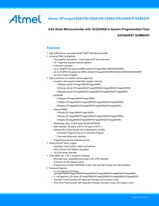
2.1 Block diagram
Figure 2-1. Block diagram.
The AVR core combines a rich instruction set with 32 general purpose working registers. All the 32 registers are
directly connected to the Arithmetic Logic Unit (ALU), allowing two independent registers to be accessed in one
PROGRAM
COUNTER
INTERNAL
OSCILLATOR
WATCHDOG
TIMER
STACK
POINTER
PROGRAM
FLASH
MCU CONTROL
REGISTER
SRAM
GENERAL
PURPOSE
REGISTERS
INSTRUCTION
REGISTER
TIMER/
COUNTERS
INSTRUCTION
DECODER
DATA DIR.
REG. PORTB
DATA DIR.
REG. PORTE
DATA DIR.
REG. PORTA
DATA DIR.
REG. PORTD
DATA REGISTER
PORTB
DATA REGISTER
PORTE
DATA REGISTER
PORTA
DATA REGISTER
PORTD
TIMING AND
CONTROL
OSCILLATOR
INTERRUPT
UNIT
EEPROM
SPI
USART
STATUS
REGISTER
Z
Y
X
ALU
PORTB DRIVERS
PORTE DRIVERS
PORTA DRIVERS
PORTF DRIVERS
PORTD DRIVERS
PORTC DRIVERS
PB0 - PB7
PE0 - PE7
PA0 - PA7
PF0 - PF7
VCC
GND
XTAL1
XTAL2
CONTROL
LINES
+
-
ANALOG
COMPARATOR
PC0 - PC7
8-BIT DATA BUS
RESET
CALIB. OSC
DATA DIR.
REG. PORTC
DATA REGISTER
PORTC
ON-CHIP DEBUG
JTAG TAP
PROGRAMMING
LOGIC
BOUNDARY-
SCAN
DATA DIR.
REG. PORTF
DATA REGISTER
PORTF
ADC
PD0 - PD7
DATA DIR.
REG. PORTG
DATA REG.
PORTG
PORTG DRIVERS
PG0 - PG4
AGND
AREF
AVCC
UNIVERSAL
SERIAL INTERFACE
AVR CPU
LCD
CONTROLLER/
DRIVER
PORTH
DRIVERS
PH0
-
PH7
DATA
DIR.
REG.
PORTH
DATA
REGISTER
PORTH
PORTJ
DRIVERS
PJ0
-
PJ6
DATA
DIR.
REG.
PORTJ
DATA
REGISTER
PORTJ
7. 7
ATmega169A/PA/329A/PA/649A/P/3290A/PA/6490A/P [DATASHEET SUMMARY]
8284FS–AVR–07/2014
single instruction executed in one clock cycle. The resulting architecture is more code efficient while achieving
throughputs up to ten times faster than conventional CISC microcontrollers.
The Atmel ATmega169A/169PA/329A/329PA/3290A/3290PA/649A/649P/6490A/6490P provides the following
features: 16K/32K/64K bytes of In-System Programmable Flash with Read-While-Write capabilities, 512/1K/2K
bytes EEPROM, 1K/2K/4K byte SRAM, 54/69 general purpose I/O lines, 32 general purpose working registers, a
JTAG interface for Boundary-scan, On-chip Debugging support and programming, a complete On-chip LCD
controller with internal contrast control, three flexible Timer/Counters with compare modes, internal and external
interrupts, a serial programmable USART, Universal Serial Interface with Start Condition Detector, an 8-channel,
10-bit ADC, a programmable Watchdog Timer with internal Oscillator, an SPI serial port, and five software
selectable power saving modes. The Idle mode stops the CPU while allowing the SRAM, Timer/Counters, SPI port,
and interrupt system to continue functioning. The Power-down mode saves the register contents but freezes the
Oscillator, disabling all other chip functions until the next interrupt or hardware reset. In Power-save mode, the
asynchronous timer and the LCD controller continues to run, allowing the user to maintain a timer base and
operate the LCD display while the rest of the device is sleeping. The ADC Noise Reduction mode stops the CPU
and all I/O modules except asynchronous timer, LCD controller and ADC, to minimize switching noise during ADC
conversions. In Standby mode, the XTAL/resonator Oscillator is running while the rest of the device is sleeping.
This allows very fast start-up combined with low-power consumption.
Atmel offers the QTouch library for embedding capacitive touch buttons, sliders and wheels functionality into AVR
microcontrollers. The patented charge-transfer signal acquisition offers robust sensing and includes fully
debounced reporting of touch keys and includes Adjacent Key Suppression®
(AKS®
) technology for unambiguous
detection of key events. The easy-to-use QTouch Suite toolchain allows you to explore, develop and debug your
own touch applications.
The device is manufactured using the Atmel high density non-volatile memory technology. The On-chip In-System
re-Programmable (ISP) Flash allows the program memory to be reprogrammed In-System through an SPI serial
interface, by a conventional non-volatile memory programmer, or by an On-chip Boot program running on the AVR
core. The Boot program can use any interface to download the application program in the Application Flash
memory. Software in the Boot Flash section will continue to run while the Application Flash section is updated,
providing true Read-While-Write operation.
By combining an 8-bit RISC CPU with In-System Self-Programmable Flash on a monolithic chip, the
ATmega169A/169PA/329A/329PA/3290A/3290PA/649A/649P/6490A/6490P is a powerful microcontroller that
provides a highly flexible and cost effective solution to many embedded control applications.
The ATmega169A/169PA/329A/329PA/3290A/3290PA/649A/649P/6490A/6490P AVR is supported with a full
suite of program and system development tools including: C Compilers, Macro Assemblers, Program
Debugger/Simulators, In-Circuit Emulators, and Evaluation kits.
9. 9
ATmega169A/PA/329A/PA/649A/P/3290A/PA/6490A/P [DATASHEET SUMMARY]
8284FS–AVR–07/2014
2.3 Pin descriptions
The following section describes the I/O-pin special functions.
2.3.1 VCC
Digital supply voltage.
2.3.2 GND
Ground.
2.3.3 Port A (PA7...PA0)
Port A is an 8-bit bi-directional I/O port with internal pull-up resistors (selected for each bit). The Port A output
buffers have symmetrical drive characteristics with both high sink and source capability. As inputs, Port A pins that
are externally pulled low will source current if the pull-up resistors are activated. The Port A pins are tri-stated when
a reset condition becomes active, even if the clock is not running.
Port A also serves the functions of various special features of the Atmel
ATmega169A/169PA/329A/329PA/3290A/3290PA/649A/649P/6490A/6490P as listed on page 72.
2.3.4 Port B (PB7...PB0)
Port B is an 8-bit bi-directional I/O port with internal pull-up resistors (selected for each bit). The Port B output
buffers have symmetrical drive characteristics with both high sink and source capability. As inputs, Port B pins that
are externally pulled low will source current if the pull-up resistors are activated. The Port B pins are tri-stated when
a reset condition becomes active, even if the clock is not running.
Port B has better driving capabilities than the other ports.
Port B also serves the functions of various special features of the
ATmega169A/169PA/329A/329PA/3290A/3290PA/649A/649P/6490A/6490P as listed on page 73.
2.3.5 Port C (PC7...PC0)
Port C is an 8-bit bi-directional I/O port with internal pull-up resistors (selected for each bit). The Port C output
buffers have symmetrical drive characteristics with both high sink and source capability. As inputs, Port C pins that
are externally pulled low will source current if the pull-up resistors are activated. The Port C pins are tri-stated when
a reset condition becomes active, even if the clock is not running.
Port C also serves the functions of special features of the
ATmega169A/169PA/329A/329PA/3290A/3290PA/649A/649P/6490A/6490P as listed on page 76.
2.3.6 Port D (PD7...PD0)
Port D is an 8-bit bi-directional I/O port with internal pull-up resistors (selected for each bit). The Port D output
buffers have symmetrical drive characteristics with both high sink and source capability. As inputs, Port D pins that
are externally pulled low will source current if the pull-up resistors are activated. The Port D pins are tri-stated when
a reset condition becomes active, even if the clock is not running.
Port D also serves the functions of various special features of the
ATmega169A/169PA/329A/329PA/3290A/3290PA/649A/649P/6490A/6490P as listed on page 77.
2.3.7 Port E (PE7...PE0)
Port E is an 8-bit bi-directional I/O port with internal pull-up resistors (selected for each bit). The Port E output
buffers have symmetrical drive characteristics with both high sink and source capability. As inputs, Port E pins that
10. 10
ATmega169A/PA/329A/PA/649A/P/3290A/PA/6490A/P [DATASHEET SUMMARY]
8284FS–AVR–07/2014
are externally pulled low will source current if the pull-up resistors are activated. The Port E pins are tri-stated when
a reset condition becomes active, even if the clock is not running.
Port E also serves the functions of various special features of the
ATmega169A/169PA/329A/329PA/3290A/3290PA/649A/649P/6490A/6490P as listed on page 79.
2.3.8 Port F (PF7...PF0)
Port F serves as the analog inputs to the A/D Converter.
Port F also serves as an 8-bit bi-directional I/O port, if the A/D Converter is not used. Port pins can provide internal
pull-up resistors (selected for each bit). The Port F output buffers have symmetrical drive characteristics with both
high sink and source capability. As inputs, Port F pins that are externally pulled low will source current if the pull-up
resistors are activated. The Port F pins are tri-stated when a reset condition becomes active, even if the clock is not
running. If the JTAG interface is enabled, the pull-up resistors on pins PF7(TDI), PF5(TMS), and PF4(TCK) will be
activated even if a reset occurs.
Port F also serves the functions of the JTAG interface.
2.3.9 Port G (PG5...PG0)
Port G is a 6-bit bi-directional I/O port with internal pull-up resistors (selected for each bit). The Port G output
buffers have symmetrical drive characteristics with both high sink and source capability. As inputs, Port G pins that
are externally pulled low will source current if the pull-up resistors are activated. The Port G pins are tri-stated
when a reset condition becomes active, even if the clock is not running.
Port G also serves the functions of various special features of the
ATmega169A/169PA/329A/329PA/3290A/3290PA/649A/649P/6490A/6490P as listed on page 83.
2.3.10 Port H (PH7...PH0)
Port H is a 8-bit bi-directional I/O port with internal pull-up resistors (selected for each bit). The Port H output
buffers have symmetrical drive characteristics with both high sink and source capability. As inputs, Port H pins that
are externally pulled low will source current if the pull-up resistors are activated. The Port H pins are tri-stated when
a reset condition becomes active, even if the clock is not running.
Port H also serves the functions of various special features of the ATmega3290PA/6490P as listed on page 85.
2.3.11 Port J (PJ6...PJ0)
Port J is a 7-bit bi-directional I/O port with internal pull-up resistors (selected for each bit). The Port J output buffers
have symmetrical drive characteristics with both high sink and source capability. As inputs, Port J pins that are
externally pulled low will source current if the pull-up resistors are activated. The Port J pins are tri-stated when a
reset condition becomes active, even if the clock is not running.
Port J also serves the functions of various special features of the ATmega3290PA/6490P as listed on page 87.
2.3.12 RESET
Reset input. A low level on this pin for longer than the minimum pulse length will generate a reset, even if the clock
is not running. The minimum pulse length is given in ”System and reset characteristics” on page 332. Shorter
pulses are not guaranteed to generate a reset.
2.3.13 XTAL1
Input to the inverting Oscillator amplifier and input to the internal clock operating circuit.
2.3.14 XTAL2
Output from the inverting Oscillator amplifier.
11. 11
ATmega169A/PA/329A/PA/649A/P/3290A/PA/6490A/P [DATASHEET SUMMARY]
8284FS–AVR–07/2014
2.3.15 AVCC
AVCC is the supply voltage pin for Port F and the A/D Converter. It should be externally connected to VCC, even if
the ADC is not used. If the ADC is used, it should be connected to VCC through a low-pass filter.
2.3.16 AREF
This is the analog reference pin for the A/D Converter.
2.3.17 LCDCAP
An external capacitor (typical > 470 nF) must be connected to the LCDCAP pin as shown in Figure 24-2, if the LCD
module is enabled and configured to use internal power. This capacitor acts as a reservoir for LCD power (VLCD). A
large capacitance reduces ripple on VLCD but increases the time until VLCD reaches its target value.
12. 12
ATmega169A/PA/329A/PA/649A/P/3290A/PA/6490A/P [DATASHEET SUMMARY]
8284FS–AVR–07/2014
3. Resources
A comprehensive set of development tools, application notes and datasheets are available for download on
http://www.atmel.com/avr.
Note: 1.
4. Data retention
Reliability Qualification results show that the projected data retention failure rate is much less than 1 PPM over 20
years at 85°C or 100 years at 25°C.
5. About code examples
This documentation contains simple code examples that briefly show how to use various parts of the device. These
code examples assume that the part specific header file is included before compilation. Be aware that not all C
compiler vendors include bit definitions in the header files and interrupt handling in C is compiler dependent.
Please confirm with the C compiler documentation for more details.
For I/O Registers located in extended I/O map, “IN”, “OUT”, “SBIS”, “SBIC”, “CBI”, and “SBI” instructions must be
replaced with instructions that allow access to extended I/O. Typically “LDS” and “STS” combined with “SBRS”,
“SBRC”, “SBR”, and “CBR”.
6. Capacitive touch sensing
The Atmel®
QTouch®
Library provides a simple to use solution to realize touch sensitive interfaces on most Atmel
AVR®
microcontrollers. The QTouch Library includes support for the QTouch and QMatrix®
acquisition methods.
Touch sensing can be added to any application by linking the appropriate Atmel QTouch Library for the AVR
Microcontroller. This is done by using a simple set of APIs to define the touch channels and sensors, and then
calling the touch sensing API’s to retrieve the channel information and determine the touch sensor states.
The QTouch Library is FREE and downloadable from the Atmel website at the following location:
www.atmel.com/qtouchlibrary. For implementation details and other information, refer to the Atmel QTouch Library
User Guide - also available for download from the Atmel website.
7. Register summary
Note: Registers with bold type only available in Atmel ATmega3290A/3290PA/6490A/6490P.
Address Name Bit 7 Bit 6 Bit 5 Bit 4 Bit 3 Bit 2 Bit 1 Bit 0 Page
(0xFF) LCDDR19 SEG339 SEG338 SEG337 SEG336 SEG335 SEG334 SEG333 SEG332 236
(0xFE) LCDDR18 SEG331 SEG330 SEG329 SEG328 SEG327 SEG326 SEG325 SEG324 236
(0xFD) LCDDR17 SEG323 SEG322 SEG321 SEG320 SEG319 SEG318 SEG317 SEG316 236
(0xFC) LCDDR16 SEG315 SEG314 SEG313 SEG312 SEG311 SEG310 SEG309 SEG308 236
(0xFB) LCDDR15 SEG307 SEG306 SEG305 SEG304 SEG303 SEG302 SEG301 SEG300 236
(0xFA) LCDDR14 SEG239 SEG238 SEG237 SEG236 SEG235 SEG234 SEG233 SEG232 236
(0xF9) LCDDR13 SEG231 SEG230 SEG229 SEG228 SEG227 SEG226 SEG225 SEG224 236
(0xF8) LCDDR12 SEG223 SEG222 SEG221 SEG220 SEG219 SEG218 SEG217 SEG216 236
(0xF7) LCDDR11 SEG215 SEG214 SEG213 SEG212 SEG211 SEG210 SEG209 SEG208 236
(0xF6) LCDDR10 SEG207 SEG206 SEG205 SEG204 SEG203 SEG202 SEG201 SEG200 236
(0xF5) LCDDR09 SEG139 SEG138 SEG137 SEG136 SEG135 SEG134 SEG133 SEG132 236
16. 16
ATmega169A/PA/329A/PA/649A/P/3290A/PA/6490A/P [DATASHEET SUMMARY]
8284FS–AVR–07/2014
Notes: 1. For compatibility with future devices, reserved bits should be written to zero if accessed. Reserved I/O memory addresses
should never be written.
2. I/O Registers within the address range 0x00 - 0x1F are directly bit-accessible using the SBI and CBI instructions. In these
registers, the value of single bits can be checked by using the SBIS and SBIC instructions.
3. Some of the Status Flags are cleared by writing a logical one to them. Note that, unlike most other AVRs, the CBI and SBI
instructions will only operate on the specified bit, and can therefore be used on registers containing such Status Flags. The
CBI and SBI instructions work with registers 0x00 to 0x1F only.
4. When using the I/O specific commands IN and OUT, the I/O addresses 0x00 - 0x3F must be used. When addressing I/O
Registers as data space using LD and ST instructions, 0x20 must be added to these addresses. The Atmel
ATmega169A/169PA/329A/329PA/3290A/3290PA/649A/649P/6490A/6490P is a complex microcontroller with more
peripheral units than can be supported within the 64 location reserved in Opcode for the IN and OUT instructions. For the
Extended I/O space from 0x60 - 0xFF in SRAM, only the ST/STS/STD and LD/LDS/LDD instructions can be used.
0x11 (0x31) PORTF PORTF7 PORTF6 PORTF5 PORTF4 PORTF3 PORTF2 PORTF1 PORTF0 92
0x10 (0x30) DDRF DDF7 DDF6 DDF5 DDF4 DDF3 DDF2 DDF1 DDF0 92
0x0F (0x2F) PINF PINF7 PINF6 PINF5 PINF4 PINF3 PINF2 PINF1 PINF0 92
0x0E (0x2E) PORTE PORTE7 PORTE6 PORTE5 PORTE4 PORTE3 PORTE2 PORTE1 PORTE0 91
0x0D (0x2D) DDRE DDE7 DDE6 DDE5 DDE4 DDE3 DDE2 DDE1 DDE0 92
0x0C (0x2C) PINE PINE7 PINE6 PINE5 PINE4 PINE3 PINE2 PINE1 PINE0 92
0x0B (0x2B) PORTD PORTD7 PORTD6 PORTD5 PORTD4 PORTD3 PORTD2 PORTD1 PORTD0 91
0x0A (0x2A) DDRD DDD7 DDD6 DDD5 DDD4 DDD3 DDD2 DDD1 DDD0 91
0x09 (0x29) PIND PIND7 PIND6 PIND5 PIND4 PIND3 PIND2 PIND1 PIND0 91
0x08 (0x28) PORTC PORTC7 PORTC6 PORTC5 PORTC4 PORTC3 PORTC2 PORTC1 PORTC0 91
0x07 (0x27) DDRC DDC7 DDC6 DDC5 DDC4 DDC3 DDC2 DDC1 DDC0 91
0x06 (0x26) PINC PINC7 PINC6 PINC5 PINC4 PINC3 PINC2 PINC1 PINC0 91
0x05 (0x25) PORTB PORTB7 PORTB6 PORTB5 PORTB4 PORTB3 PORTB2 PORTB1 PORTB0 90
0x04 (0x24) DDRB DDB7 DDB6 DDB5 DDB4 DDB3 DDB2 DDB1 DDB0 90
0x03 (0x23) PINB PINB7 PINB6 PINB5 PINB4 PINB3 PINB2 PINB1 PINB0 91
0x02 (0x22) PORTA PORTA7 PORTA6 PORTA5 PORTA4 PORTA3 PORTA2 PORTA1 PORTA0 90
0x01 (0x21) DDRA DDA7 DDA6 DDA5 DDA4 DDA3 DDA2 DDA1 DDA0 90
0x00 (0x20) PINA PINA7 PINA6 PINA5 PINA4 PINA3 PINA2 PINA1 PINA0 90
Address Name Bit 7 Bit 6 Bit 5 Bit 4 Bit 3 Bit 2 Bit 1 Bit 0 Page
17. 17
ATmega169A/PA/329A/PA/649A/P/3290A/PA/6490A/P [DATASHEET SUMMARY]
8284FS–AVR–07/2014
8. Instruction set summary
Mnemonics Operands Description Operation Flags #Clocks
ARITHMETIC AND LOGIC INSTRUCTIONS
ADD Rd, Rr Add two Registers Rd ← Rd + Rr Z,C,N,V,H 1
ADC Rd, Rr Add with Carry two Registers Rd ← Rd + Rr + C Z,C,N,V,H 1
ADIW Rdl,K Add Immediate to Word Rdh:Rdl ← Rdh:Rdl + K Z,C,N,V,S 2
SUB Rd, Rr Subtract two Registers Rd ← Rd - Rr Z,C,N,V,H 1
SUBI Rd, K Subtract Constant from Register Rd ← Rd - K Z,C,N,V,H 1
SBC Rd, Rr Subtract with Carry two Registers Rd ← Rd - Rr - C Z,C,N,V,H 1
SBCI Rd, K Subtract with Carry Constant from Reg. Rd ← Rd - K - C Z,C,N,V,H 1
SBIW Rdl,K Subtract Immediate from Word Rdh:Rdl ← Rdh:Rdl - K Z,C,N,V,S 2
AND Rd, Rr Logical AND Registers Rd ← Rd • Rr Z,N,V 1
ANDI Rd, K Logical AND Register and Constant Rd ← Rd • K Z,N,V 1
OR Rd, Rr Logical OR Registers Rd ← Rd v Rr Z,N,V 1
ORI Rd, K Logical OR Register and Constant Rd ← Rd v K Z,N,V 1
EOR Rd, Rr Exclusive OR Registers Rd ← Rd ⊕ Rr Z,N,V 1
COM Rd One’s Complement Rd ← 0xFF − Rd Z,C,N,V 1
NEG Rd Two’s Complement Rd ← 0x00 − Rd Z,C,N,V,H 1
SBR Rd,K Set Bit(s) in Register Rd ← Rd v K Z,N,V 1
CBR Rd,K Clear Bit(s) in Register Rd ← Rd • (0xFF - K) Z,N,V 1
INC Rd Increment Rd ← Rd + 1 Z,N,V 1
DEC Rd Decrement Rd ← Rd − 1 Z,N,V 1
TST Rd Test for Zero or Minus Rd ← Rd • Rd Z,N,V 1
CLR Rd Clear Register Rd ← Rd ⊕ Rd Z,N,V 1
SER Rd Set Register Rd ← 0xFF None 1
MUL Rd, Rr Multiply Unsigned R1:R0 ← Rd x Rr Z,C 2
MULS Rd, Rr Multiply Signed R1:R0 ← Rd x Rr Z,C 2
MULSU Rd, Rr Multiply Signed with Unsigned R1:R0 ← Rd x Rr Z,C 2
FMUL Rd, Rr Fractional Multiply Unsigned R1:R0 ← (Rd x Rr) << 1 Z,C 2
FMULS Rd, Rr Fractional Multiply Signed R1:R0 ← (Rd x Rr) << 1 Z,C 2
FMULSU Rd, Rr Fractional Multiply Signed with Unsigned R1:R0 ← (Rd x Rr) << 1 Z,C 2
BRANCH INSTRUCTIONS
RJMP k Relative Jump PC ← PC + k + 1 None 2
IJMP Indirect Jump to (Z) PC ← Z None 2
JMP k Direct Jump PC ← k None 3
RCALL k Relative Subroutine Call PC ← PC + k + 1 None 3
ICALL Indirect Call to (Z) PC ← Z None 3
CALL k Direct Subroutine Call PC ← k None 4
RET Subroutine Return PC ← STACK None 4
RETI Interrupt Return PC ← STACK I 4
CPSE Rd,Rr Compare, Skip if Equal if (Rd = Rr) PC ← PC + 2 or 3 None 1/2/3
CP Rd,Rr Compare Rd − Rr Z, N,V,C,H 1
CPC Rd,Rr Compare with Carry Rd − Rr − C Z, N,V,C,H 1
CPI Rd,K Compare Register with Immediate Rd − K Z, N,V,C,H 1
SBRC Rr, b Skip if Bit in Register Cleared if (Rr(b)=0) PC ← PC + 2 or 3 None 1/2/3
SBRS Rr, b Skip if Bit in Register is Set if (Rr(b)=1) PC ← PC + 2 or 3 None 1/2/3
SBIC P, b Skip if Bit in I/O Register Cleared if (P(b)=0) PC ← PC + 2 or 3 None 1/2/3
SBIS P, b Skip if Bit in I/O Register is Set if (P(b)=1) PC ← PC + 2 or 3 None 1/2/3
BRBS s, k Branch if Status Flag Set if (SREG(s) = 1) then PC←PC+k + 1 None 1/2
BRBC s, k Branch if Status Flag Cleared if (SREG(s) = 0) then PC←PC+k + 1 None 1/2
BREQ k Branch if Equal if (Z = 1) then PC ← PC + k + 1 None 1/2
BRNE k Branch if Not Equal if (Z = 0) then PC ← PC + k + 1 None 1/2
BRCS k Branch if Carry Set if (C = 1) then PC ← PC + k + 1 None 1/2
BRCC k Branch if Carry Cleared if (C = 0) then PC ← PC + k + 1 None 1/2
BRSH k Branch if Same or Higher if (C = 0) then PC ← PC + k + 1 None 1/2
BRLO k Branch if Lower if (C = 1) then PC ← PC + k + 1 None 1/2
BRMI k Branch if Minus if (N = 1) then PC ← PC + k + 1 None 1/2
BRPL k Branch if Plus if (N = 0) then PC ← PC + k + 1 None 1/2
BRGE k Branch if Greater or Equal, Signed if (N ⊕ V= 0) then PC ← PC + k + 1 None 1/2
BRLT k Branch if Less Than Zero, Signed if (N ⊕ V= 1) then PC ← PC + k + 1 None 1/2
BRHS k Branch if Half Carry Flag Set if (H = 1) then PC ← PC + k + 1 None 1/2
BRHC k Branch if Half Carry Flag Cleared if (H = 0) then PC ← PC + k + 1 None 1/2
BRTS k Branch if T Flag Set if (T = 1) then PC ← PC + k + 1 None 1/2
BRTC k Branch if T Flag Cleared if (T = 0) then PC ← PC + k + 1 None 1/2
BRVS k Branch if Overflow Flag is Set if (V = 1) then PC ← PC + k + 1 None 1/2
18. 18
ATmega169A/PA/329A/PA/649A/P/3290A/PA/6490A/P [DATASHEET SUMMARY]
8284FS–AVR–07/2014
BRVC k Branch if Overflow Flag is Cleared if (V = 0) then PC ← PC + k + 1 None 1/2
BRIE k Branch if Interrupt Enabled if ( I = 1) then PC ← PC + k + 1 None 1/2
BRID k Branch if Interrupt Disabled if ( I = 0) then PC ← PC + k + 1 None 1/2
BIT AND BIT-TEST INSTRUCTIONS
SBI P,b Set Bit in I/O Register I/O(P,b) ← 1 None 2
CBI P,b Clear Bit in I/O Register I/O(P,b) ← 0 None 2
LSL Rd Logical Shift Left Rd(n+1) ← Rd(n), Rd(0) ← 0 Z,C,N,V 1
LSR Rd Logical Shift Right Rd(n) ← Rd(n+1), Rd(7) ← 0 Z,C,N,V 1
ROL Rd Rotate Left Through Carry Rd(0)←C,Rd(n+1)← Rd(n),C←Rd(7) Z,C,N,V 1
ROR Rd Rotate Right Through Carry Rd(7)←C,Rd(n)← Rd(n+1),C←Rd(0) Z,C,N,V 1
ASR Rd Arithmetic Shift Right Rd(n) ← Rd(n+1), n=0..6 Z,C,N,V 1
SWAP Rd Swap Nibbles Rd(3..0)←Rd(7..4),Rd(7..4)←Rd(3..0) None 1
BSET s Flag Set SREG(s) ← 1 SREG(s) 1
BCLR s Flag Clear SREG(s) ← 0 SREG(s) 1
BST Rr, b Bit Store from Register to T T ← Rr(b) T 1
BLD Rd, b Bit load from T to Register Rd(b) ← T None 1
SEC Set Carry C ← 1 C 1
CLC Clear Carry C ← 0 C 1
SEN Set Negative Flag N ← 1 N 1
CLN Clear Negative Flag N ← 0 N 1
SEZ Set Zero Flag Z ← 1 Z 1
CLZ Clear Zero Flag Z ← 0 Z 1
SEI Global Interrupt Enable I ← 1 I 1
CLI Global Interrupt Disable I ← 0 I 1
SES Set Signed Test Flag S ← 1 S 1
CLS Clear Signed Test Flag S ← 0 S 1
SEV Set Twos Complement Overflow. V ← 1 V 1
CLV Clear Twos Complement Overflow V ← 0 V 1
SET Set T in SREG T ← 1 T 1
CLT Clear T in SREG T ← 0 T 1
SEH Set Half Carry Flag in SREG H ← 1 H 1
CLH Clear Half Carry Flag in SREG H ← 0 H 1
DATA TRANSFER INSTRUCTIONS
MOV Rd, Rr Move Between Registers Rd ← Rr None 1
MOVW Rd, Rr Copy Register Word Rd+1:Rd ← Rr+1:Rr None 1
LDI Rd, K Load Immediate Rd ← K None 1
LD Rd, X Load Indirect Rd ← (X) None 2
LD Rd, X+ Load Indirect and Post-Inc. Rd ← (X), X ← X + 1 None 2
LD Rd, - X Load Indirect and Pre-Dec. X ← X - 1, Rd ← (X) None 2
LD Rd, Y Load Indirect Rd ← (Y) None 2
LD Rd, Y+ Load Indirect and Post-Inc. Rd ← (Y), Y ← Y + 1 None 2
LD Rd, - Y Load Indirect and Pre-Dec. Y ← Y - 1, Rd ← (Y) None 2
LDD Rd,Y+q Load Indirect with Displacement Rd ← (Y + q) None 2
LD Rd, Z Load Indirect Rd ← (Z) None 2
LD Rd, Z+ Load Indirect and Post-Inc. Rd ← (Z), Z ← Z+1 None 2
LD Rd, -Z Load Indirect and Pre-Dec. Z ← Z - 1, Rd ← (Z) None 2
LDD Rd, Z+q Load Indirect with Displacement Rd ← (Z + q) None 2
LDS Rd, k Load Direct from SRAM Rd ← (k) None 2
ST X, Rr Store Indirect (X) ← Rr None 2
ST X+, Rr Store Indirect and Post-Inc. (X) ← Rr, X ← X + 1 None 2
ST - X, Rr Store Indirect and Pre-Dec. X ← X - 1, (X) ← Rr None 2
ST Y, Rr Store Indirect (Y) ← Rr None 2
ST Y+, Rr Store Indirect and Post-Inc. (Y) ← Rr, Y ← Y + 1 None 2
ST - Y, Rr Store Indirect and Pre-Dec. Y ← Y - 1, (Y) ← Rr None 2
STD Y+q,Rr Store Indirect with Displacement (Y + q) ← Rr None 2
ST Z, Rr Store Indirect (Z) ← Rr None 2
ST Z+, Rr Store Indirect and Post-Inc. (Z) ← Rr, Z ← Z + 1 None 2
ST -Z, Rr Store Indirect and Pre-Dec. Z ← Z - 1, (Z) ← Rr None 2
STD Z+q,Rr Store Indirect with Displacement (Z + q) ← Rr None 2
STS k, Rr Store Direct to SRAM (k) ← Rr None 2
LPM Load Program Memory R0 ← (Z) None 3
LPM Rd, Z Load Program Memory Rd ← (Z) None 3
LPM Rd, Z+ Load Program Memory and Post-Inc Rd ← (Z), Z ← Z+1 None 3
SPM Store Program Memory (Z) ← R1:R0 None -
IN Rd, P In Port Rd ← P None 1
OUT P, Rr Out Port P ← Rr None 1
PUSH Rr Push Register on Stack STACK ← Rr None 2
POP Rd Pop Register from Stack Rd ← STACK None 2
Mnemonics Operands Description Operation Flags #Clocks
20. 20
ATmega169A/PA/329A/PA/649A/P/3290A/PA/6490A/P [DATASHEET SUMMARY]
8284FS–AVR–07/2014
9. Ordering information
Notes: 1. This device can also be supplied in wafer form. Please contact your local Atmel sales office for detailed ordering information
and minimum quantities.
2. Pb-free packaging, complies to the European Directive for Restriction of Hazardous Substances (RoHS directive). Also
Halide free and fully Green.
3. For Speed vs. VCC, see Figure 29-1 on page 330.
4. Tape & Reel.
9.1 Atmel ATmega169A
Speed [MHz] (3)
Power supply Ordering code (2)
Package type (1)
Operational range
16 1.8 - 5.5V
ATmega169A-AU
ATmega169A-AUR (4)
ATmega169A-MU
ATmega169A-MUR (4)
ATmega169A-MCH
ATmega169A-MCHR (4)
64A
64A
64M1
64M1
64MC
64MC
Industrial
(-40°C to 85°C)
ATmega169A-AN
ATmega169A-ANR (4)
ATmega169A-MN
ATmega169A-MNR (4)
64A
64A
64M1
64M1
Extended
(-40°C to 105°C)
Package type
64A 64-lead, thin (1.0mm) plastic Gull Wing Quad Flat Package (TQFP)
64M1 64-pad, 9 × 9 × 1.0mm body, lead pitch 0.50mm, Quad Flat No-Lead/Micro Lead Frame Package (QFN/MLF)
64MC 64-lead (2-row Staggered), 7 × 7 × 1.0mm body, 4.0 × 4.0 mm Exposed Pad, Quad Flat No-Lead Package (QFN)
21. 21
ATmega169A/PA/329A/PA/649A/P/3290A/PA/6490A/P [DATASHEET SUMMARY]
8284FS–AVR–07/2014
9.2 Atmel ATmega169PA
Notes: 1. This device can also be supplied in wafer form. Please contact your local Atmel sales office for detailed ordering information
and minimum quantities.
2. Pb-free packaging, complies to the European Directive for Restriction of Hazardous Substances (RoHS directive). Also
Halide free and fully Green.
3. For Speed vs. VCC, see Figure 29-1 on page 330.
4. Tape & Reel.
5. See characterization specification at 105°C.
Speed [MHz] (3)
Power supply Ordering code (2)
Package type(1)
Operational range
16 1.8 - 5.5V
ATmega169PA-AU
ATmega169PA-AUR(4)
ATmega169PA-MU
ATmega169PA-MUR(4)
ATmega169PA-MCH
ATmega169PA-MCHR(4)
64A
64A
64M1
64M1
64MC
64MC
Industrial
(-40°C to 85°C)
ATmega169PA-AN
ATmega169PA-ANR(4)
ATmega169PA-MN
ATmega169PA-MNR(4)
64A
64A
64M1
64M1
Extended
(-40°C to 105°C)(5)
Package type
64A 64-lead, thin (1.0mm) plastic Gull Wing Quad Flat Package (TQFP)
64M1 64-pad, 9 × 9 × 1.0mm body, lead pitch 0.50mm, Quad Flat No-Lead/Micro Lead Frame Package (QFN/MLF)
64MC 64-lead (2-row Staggered), 7 × 7 × 1.0mm body, 4.0 × 4.0mm Exposed Pad, Quad Flat No-Lead Package (QFN)
22. 22
ATmega169A/PA/329A/PA/649A/P/3290A/PA/6490A/P [DATASHEET SUMMARY]
8284FS–AVR–07/2014
9.3 Atmel ATmega329A
Notes: 1. This device can also be supplied in wafer form. Please contact your local Atmel sales office for detailed ordering information
and minimum quantities.
2. Pb-free packaging complies to the European Directive for Restriction of Hazardous Substances (RoHS directive). Also
Halide free and fully Green.
3. For Speed vs. VCC see Figure 29-2 on page 330.
4. Tape & Reel.
5. See characterization specifications at 105°C.
Speed [MHz] (3)
Power supply Ordering code (2)
Package type (1)
Operational range
20 1.8 - 5.5V
ATmega329A-AU
ATmega329A-AUR (4)
ATmega329A-MU
ATmega329A-MUR (4)
64A
64A
64M1
64M1
Industrial
(-40°C to 85°C)
ATmega329A-AN
ATmega329A-ANR (4)
ATmega329A-MN
ATmega329A-MNR (4)
64A
64A
64M1
64M1
Extended
(-40°C to 105°C)(5)
Package type
64A 64-lead, 14 × 14 × 1.0mm, thin profile plastic Quad Flat Package (TQFP)
64M1 64-pad, 9 × 9 × 1.0mm, Quad Flat No-Lead/Micro Lead Frame Package (QFN/MLF)
23. 23
ATmega169A/PA/329A/PA/649A/P/3290A/PA/6490A/P [DATASHEET SUMMARY]
8284FS–AVR–07/2014
Notes: 1. This device can also be supplied in wafer form. Please contact your local Atmel sales office for detailed ordering information
and minimum quantities.
2. Pb-free packaging complies to the European Directive for Restriction of Hazardous Substances (RoHS directive). Also
Halide free and fully Green.
3. For Speed vs. VCC see Figure 29-2 on page 330.
4. Tape &Reel.
5. See characterization specification at 105°C.
9.4 Atmel ATmega329PA
Speed [MHz] (3)
Power supply Ordering code (2)
Package type (1)
Operational range
20 1.8 - 5.5V
ATmega329PA-AU
ATmega329PA-AUR(4)
ATmega329PA-MU
ATmega329PA-MUR(4)
64A
64A
64M1
64M1
Industrial
(-40°C to 85°C)
ATmega329PA-AN
ATmega329PA-ANR(4)
ATmega329PA-MN
ATmega329PA-MNR(4)
64A
64A
64M1
64M1
Extended
(-40°C to 105°C)(5)
Package type
64A 64-lead, 14 × 14 × 1.0mm, thin profile Plastic Quad Flat Package (TQFP)
64M1 64-pad, 9 × 9 × 1.0mm, Quad Flat No-Lead/Micro Lead Frame Package (QFN/MLF)
24. 24
ATmega169A/PA/329A/PA/649A/P/3290A/PA/6490A/P [DATASHEET SUMMARY]
8284FS–AVR–07/2014
Notes: 1. This device can also be supplied in wafer form. Please contact your local Atmel sales office for detailed ordering information
and minimum quantities.
2. Pb-free packaging complies to the European Directive for Restriction of Hazardous Substances (RoHS directive). Also
Halide free and fully Green.
3. For Speed vs. VCC see Figure 29-2 on page 330.
4. Tape & Reel.
5. See characterization specification at 105°C.
9.5 Atmel ATmega3290A
Speed [MHz] (3)
Power supply Ordering code (2)
Package type (1)
Operational range
20 1.8 - 5.5V
ATmega3290A-AU
ATmega3290A-AUR (4)
100A
100A
Industrial
(-40°C to 85°C)
ATmega3290A-AN
ATmega3290A-ANR (4)
100A
100A
Extended
(-40°C to 105°C)(5)
Package type
100A 100-lead, 14 × 14 × 1.0mm, 0.5mm Lead Pitch, Thin Profile Plastic Quad Flat Package (TQFP)
25. 25
ATmega169A/PA/329A/PA/649A/P/3290A/PA/6490A/P [DATASHEET SUMMARY]
8284FS–AVR–07/2014
Notes: 1. This device can also be supplied in wafer form. Please contact your local Atmel sales office for detailed ordering information
and minimum quantities.
2. Pb-free packaging complies to the European Directive for Restriction of Hazardous Substances (RoHS directive). Also
Halide free and fully Green.
3. For Speed vs. VCC see Figure 29-2 on page 330.
4. Tape & Reel.
5. See characterization specification at 105°C.
9.6 Atmel ATmega3290PA
Speed [MHz] (3)
Power supply Ordering code (2)
Package type (1)
Operational range
20 1.8 - 5.5V
ATmega3290PA-AU
ATmega3290PA-AUR(4)
100A
100A
Industrial
(-40°C to 85°C)
ATmega3290PA-AN
ATmega3290PA-ANR(4)
100A
100A
Industrial
(-40°C to 105°C)(5)
Package type
100A 100-lead, 14 × 14 × 1.0mm, 0.5mm Lead Pitch, Thin Profile Plastic Quad Flat Package (TQFP)
26. 26
ATmega169A/PA/329A/PA/649A/P/3290A/PA/6490A/P [DATASHEET SUMMARY]
8284FS–AVR–07/2014
9.7 Atmel ATmega649A
Notes: 1. This device can also be supplied in wafer form. Please contact your local Atmel sales office for detailed ordering information
and minimum quantities.
2. Pb-free packaging complies to the European Directive for Restriction of Hazardous Substances (RoHS directive). Also
Halide free and fully Green.
3. For Speed vs. VCC see Figure 29-1 on page 330.
4. Tape & Reel.
Speed [MHz] (3)
Power supply Ordering code (2)
Package type (1)
Operational range
16 1.8 - 5.5V
ATmega649A-AU
ATmega649A-AUR (4)
ATmega649A-MU
ATmega649A-MUR (4)
64A
64A
64M1
64M1
Industrial
(-40°C to 85°C)
Package type
64A 64-lead, 14 × 14 × 1.0mm, Thin Profile Plastic Quad Flat Package (TQFP)
64M1 64-pad, 9 × 9 × 1.0mm, Quad Flat No-Lead/Micro Lead Frame Package (QFN/MLF)
27. 27
ATmega169A/PA/329A/PA/649A/P/3290A/PA/6490A/P [DATASHEET SUMMARY]
8284FS–AVR–07/2014
9.8 Atmel ATmega649P
Notes: 1. This device can also be supplied in wafer form. Please contact your local Atmel sales office for detailed ordering information
and minimum quantities.
2. Pb-free packaging complies to the European Directive for Restriction of Hazardous Substances (RoHS directive). Also
Halide free and fully Green.
3. For Speed vs. VCC see Figure 29-1 on page 330.
4. Tape & Reel.
Speed [MHz] (3)
Power supply Ordering code (2)
Package type (1)
Operational range
16 1.8 - 5.5 V
ATmega649P-AU
ATmega649P-AUR (4)
ATmega649P-MU
ATmega649P-MUR (4)
64A
64A
64M1
64M1
Industrial
(-40°C to 85°C)
Package type
64A 64-lead, 14 × 14 × 1.0mm, Thin Profile Plastic Quad Flat Package (TQFP)
64M1 64-pad, 9 × 9 × 1.0mm, Quad Flat No-Lead/Micro Lead Frame Package (QFN/MLF)
28. 28
ATmega169A/PA/329A/PA/649A/P/3290A/PA/6490A/P [DATASHEET SUMMARY]
8284FS–AVR–07/2014
9.9 Atmel ATmega6490A
Notes: 1. This device can also be supplied in wafer form. Please contact your local Atmel sales office for detailed ordering information
and minimum quantities.
2. Pb-free packaging complies to the European Directive for Restriction of Hazardous Substances (RoHS directive). Also
Halide free and fully Green.
3. For Speed vs. VCC see Figure 29-2 on page 330.
4. Tape & Reel.
Speed [MHz] (3)
Power supply Ordering code (2)
Package type (1)
Operational range
20 1.8 - 5.5V
ATmega6490A-AU
ATmega6490A-AUR (4)
100A
100A
Industrial
(-40°C to 85°C)
Package type
100A 100-lead, 14 × 14 × 1.0mm, 0.5mm Lead Pitch, Thin Profile Plastic Quad Flat Package (TQFP)
29. 29
ATmega169A/PA/329A/PA/649A/P/3290A/PA/6490A/P [DATASHEET SUMMARY]
8284FS–AVR–07/2014
9.10 Atmel ATmega6490P
Notes: 1. This device can also be supplied in wafer form. Please contact your local Atmel sales office for detailed ordering information
and minimum quantities.
2. Pb-free packaging complies to the European Directive for Restriction of Hazardous Substances (RoHS directive). Also
Halide free and fully Green.
3. For Speed vs. VCC see Figure 29-2 on page 330.
4. Tape & Reel.
Speed [MHz] (3)
Power supply Ordering code (2)
Package type (1)
Operational range
20 1.8 - 5.5V
ATmega6490P-AU
ATmega6490P-AUR (4)
100A
100A
Industrial
(-40°C to 85°C)
Package Type
100A 100-lead, 14 × 14 × 1.0mm, 0.5mm Lead Pitch, Thin Profile Plastic Quad Flat Package (TQFP)
30. 30
ATmega169A/PA/329A/PA/649A/P/3290A/PA/6490A/P [DATASHEET SUMMARY]
8284FS–AVR–07/2014
10. Packaging Information
10.1 64A
2325 Orchard Parkway
San Jose, CA 95131
TITLE DRAWING NO. REV.
64A, 64-lead, 14 x 14mm Body Size, 1.0mm Body Thickness,
0.8mm Lead Pitch, Thin Profile Plastic Quad Flat Package (TQFP)
C
64A
2010-10-20
PIN 1 IDENTIFIER
0°~7°
PIN 1
L
C
A1 A2 A
D1
D
e
E1 E
B
COMMON DIMENSIONS
(Unit of measure = mm)
SYMBOL MIN NOM MAX NOTE
Notes:
1.This package conforms to JEDEC reference MS-026, Variation AEB.
2. Dimensions D1 and E1 do not include mold protrusion. Allowable
protrusion is 0.25mm per side. Dimensions D1 and E1 are maximum
plastic body size dimensions including mold mismatch.
3. Lead coplanarity is 0.10mm maximum.
A – – 1.20
A1 0.05 – 0.15
A2 0.95 1.00 1.05
D 15.75 16.00 16.25
D1 13.90 14.00 14.10 Note 2
E 15.75 16.00 16.25
E1 13.90 14.00 14.10 Note 2
B 0.30– 0.45
C 0.09 – 0.20
L 0.45 – 0.75
e 0.80 TYP
31. 31
ATmega169A/PA/329A/PA/649A/P/3290A/PA/6490A/P [DATASHEET SUMMARY]
8284FS–AVR–07/2014
10.2 64M1
2325 Orchard Parkway
San Jose, CA 95131
TITLE DRAWING NO. REV.
64M1, 64-pad, 9 x 9 x 1.0 mm Body, Lead Pitch 0.50 mm, H
64M1
2010-10-19
COMMON DIMENSIONS
(Unit of Measure = mm)
SYMBOL MIN NOM MAX NOTE
A 0.80 0.90 1.00
A1 – 0.02 0.05
b 0.18 0.25 0.30
D
D2 5.20 5.40 5.60
8.90 9.00 9.10
8.90 9.00 9.10
E
E2 5.20 5.40 5.60
e 0.50 BSC
L 0.35 0.40 0.45
Notes:
1. JEDEC Standard MO-220, (SAW Singulation) Fig. 1, VMMD.
2. Dimension and tolerance conform to ASMEY14.5M-1994.
TOP VIEW
SIDE VIEW
BOTTOM VIEW
D
E
Marked Pin# 1 ID
SEATING PLANE
A1
C
A
C
0.08
1
2
3
K 1.25 1.40 1.55
E2
D2
b e
Pin #1 Corner
L
Pin #1
Triangle
Pin #1
Chamfer
(C 0.30)
Option A
Option B
Pin #1
Notch
(0.20 R)
Option C
K
K
5.40 mm Exposed Pad, Micro Lead Frame Package (MLF)
32. 32
ATmega169A/PA/329A/PA/649A/P/3290A/PA/6490A/P [DATASHEET SUMMARY]
8284FS–AVR–07/2014
10.3 64MC
TITLE DRAWING NO.
GPC REV.
Package Drawing Contact:
packagedrawings@atmel.com 64MC
ZXC A
64MC, 64QFN (2-Row Staggered),
7 x 7 x 1.00 mm Body, 4.0 x 4.0 mm Exposed Pad,
Quad Flat No Lead Package
10/3/07
COMMON DIMENSIONS
(Unit of Measure = mm)
SYMBOL MIN NOM MAX NOTE
A 0.80 0.90 1.00
A1 0.00 0.02 0.05
b 0.18 0.23 0.28
C 0.20 REF
D 6.90 7.00 7.10
D2 3.95 4.00 4.05
E 6.90 7.00 7.10
E2 3.95 4.00 4.05
eT – 0.65 –
eR – 0.65 –
K 0.20 – – (REF)
L 0.35 0.40 0.45
y 0.00 – 0.075
SIDE VIEW
TOP VIEW
BOTTOM VIEW
Note: 1. The terminal #1 ID is a Laser-marked Feature.
Pin 1 ID
D
E
A1
A
y
C
eT/2
R0.20 0.40
B1
A1
B30
A34
b
A8
B7
eT
D2
B16
A18
B22
A25
E2 K (0.1) REF
B8
A9
(0.18) REF
L
B15
A17
L
eR
A26
B23
eT
33. 33
ATmega169A/PA/329A/PA/649A/P/3290A/PA/6490A/P [DATASHEET SUMMARY]
8284FS–AVR–07/2014
10.4 100A
100A, 100-lead, 14 x 14mm Body Size, 1.0mm Body Thickness,
0.5mm Lead Pitch, Thin Profile Plastic Quad Flat Package (TQFP) 100A E
2014-02-05
PIN 1 IDENTIFIER
0°~7°
PIN 1
L
C
A1 A2 A
D1
D
e E1 E
B
A – – 1.20
A1 0.05 – 0.15
A2 0.95 1.00 1.05
D 15.75 16.00 16.25
D1 13.90 14.00 14.10 Note 2
E 15.75 16.00 16.25
E1 13.90 14.00 14.10 Note 2
B 0.17 – 0.27
C 0.09 – 0.20
L 0.45 – 0.75
e 0.50 TYP
Notes:
1. This package conforms to JEDEC reference MS-026, Variation AED.
2. Dimensions D1 and E1 do not include mold protrusion. Allowable
protrusion is 0.25mm per side. Dimensions D1 and E1 are maximum
plastic body size dimensions including mold mismatch.
3. Lead coplanarity is 0.08mm maximum.
COMMON DIMENSIONS
(Unit of Measure = mm)
SYMBOL MIN NOM MAX NOTE
34. 34
ATmega169A/PA/329A/PA/649A/P/3290A/PA/6490A/P [DATASHEET SUMMARY]
8284FS–AVR–07/2014
11. Errata
11.1 Atmel ATmega169A
No known errata
11.2 Atmel ATmega169A/169PA Rev. A to F
Not sampled.
11.3 Atmel ATmega169PA Rev. G
No known errata.
11.4 Atmel ATmega329A/329PA rev. A
• Interrupts may be lost when writing the timer registers in the asynchronous timer
• Using BOD disable will make the chip reset
1. Interrupts may be lost when writing the timer registers in the asynchronous timer
The interrupt will be lost if a timer register that is synchronous timer clock is written when the asynchronous
Timer/Counter register (TCNTx) is 0x00.
Problem Fix/ Workaround
Always check that the asynchronous Timer/Counter register neither have the value 0xFF nor 0x00 before writ-
ing to the asynchronous Timer Control Register (TCCRx), asynchronous Timer Counter Register (TCNTx), or
asynchronous Output Compare Register (OCRx).
2. Using BOD disable will make the chip reset
If the part enters sleep with the BOD turned off with the BOD disable option
enabled, a BOD reset will be generated at wakeup and the chip will reset.
Problem Fix/Workaround
Do not use BOD disable
11.5 Atmel ATmega329A/329PA rev. B
• Interrupts may be lost when writing the timer registers in the asynchronous timer
1. Interrupts may be lost when writing the timer registers in the asynchronous timer
The interrupt will be lost if a timer register that is synchronous timer clock is written when the asynchronous
Timer/Counter register (TCNTx) is 0x00.
Problem Fix/ Workaround
Always check that the asynchronous Timer/Counter register neither have the value 0xFF nor 0x00 before writ-
ing to the asynchronous Timer Control Register (TCCRx), asynchronous Timer Counter Register (TCNTx), or
asynchronous Output Compare Register (OCRx).
35. 35
ATmega169A/PA/329A/PA/649A/P/3290A/PA/6490A/P [DATASHEET SUMMARY]
8284FS–AVR–07/2014
11.6 Atmel ATmega329A/329PA rev. C
• Interrupts may be lost when writing the timer registers in the asynchronous timer
1. Interrupts may be lost when writing the timer registers in the asynchronous timer
The interrupt will be lost if a timer register that is synchronous timer clock is written when the asynchronous
Timer/Counter register (TCNTx) is 0x00.
Problem Fix/ Workaround
Always check that the asynchronous Timer/Counter register neither have the value 0xFF nor 0x00 before writ-
ing to the asynchronous Timer Control Register (TCCRx), asynchronous Timer Counter Register (TCNTx), or
asynchronous Output Compare Register (OCRx).
11.7 Atmel ATmega3290A/3290PA rev. A
• Interrupts may be lost when writing the timer registers in the asynchronous timer
• Using BOD disable will make the chip reset
1. Interrupts may be lost when writing the timer registers in the asynchronous timer
The interrupt will be lost if a timer register that is synchronous timer clock is written when the asynchronous
Timer/Counter register (TCNTx) is 0x00.
Problem Fix/ Workaround
Always check that the asynchronous Timer/Counter register neither have the value 0xFF nor 0x00 before writ-
ing to the asynchronous Timer Control Register (TCCRx), asynchronous Timer Counter Register (TCNTx), or
asynchronous Output Compare Register (OCRx).
2. Using BOD disable will make the chip reset
If the part enters sleep with the BOD turned off with the BOD disable option
enabled, a BOD reset will be generated at wakeup and the chip will reset.
Problem Fix/Workaround
Do not use BOD disable
11.8 Atmel ATmega3290A/3290PA rev. B
• Interrupts may be lost when writing the timer registers in the asynchronous timer
1. Interrupts may be lost when writing the timer registers in the asynchronous timer
The interrupt will be lost if a timer register that is synchronous timer clock is written when the asynchronous
Timer/Counter register (TCNTx) is 0x00.
Problem Fix/ Workaround
Always check that the asynchronous Timer/Counter register neither have the value 0xFF nor 0x00 before writ-
ing to the asynchronous Timer Control Register (TCCRx), asynchronous Timer Counter Register (TCNTx), or
asynchronous Output Compare Register (OCRx).
36. 36
ATmega169A/PA/329A/PA/649A/P/3290A/PA/6490A/P [DATASHEET SUMMARY]
8284FS–AVR–07/2014
11.9 Atmel ATmega3290A/3290PA rev. C
• Interrupts may be lost when writing the timer registers in the asynchronous timer
1. Interrupts may be lost when writing the timer registers in the asynchronous timer
The interrupt will be lost if a timer register that is synchronous timer clock is written when the asynchronous
Timer/Counter register (TCNTx) is 0x00.
Problem Fix/ Workaround
Always check that the asynchronous Timer/Counter register neither have the value 0xFF nor 0x00 before writ-
ing to the asynchronous Timer Control Register (TCCRx), asynchronous Timer Counter Register (TCNTx), or
asynchronous Output Compare Register (OCRx).
11.10 Atmel ATmega649A/649P/ATmega6490A/6490P
No known errata.
37. 37
ATmega169A/PA/329A/PA/649A/P/3290A/PA/6490A/P [DATASHEET SUMMARY]
8284FS–AVR–07/2014
12. Datasheet revision history
Please note that the referring page numbers in this section are referring to this document.The referring revision in
this section are referring to the document revision.
12.1 Rev. 8284F - 08/2014
12.2 Rev. 8284E - 02/2013
12.3 Rev. 8284D - 06/11
12.4 Rev. 8284C - 06/11
1. New back page
2. Changed chip references in the text in Section 9.6 ”Low-frequency XTAL oscillator” on page 34.
1. New template
2. Countless, small corrections made throughout the whole document
3.
In Section ”System and reset characteristics” on page 332 the sentence “The following chara apply only
to...” has been deleted
4.
Former Section 29.6 on page 332 (“Power-on reset”), subsection 29.6.1
(“ATmega169A/169PA/329A/329PA/3290A/3290PA/649A/649P/6490A/6490PA revision C and later”) and
subsection 29.6.2 (“ATmega329A/329PA/3290A/3290PA/649A/649P/6490A/6490PA revision A and B”)
have been deleted
5. The maximum limits for “Power Supply Current” in Table 29-9 on page 328 have been corrected
6. The maximum limits for “Power Supply Current” in Table 29-11 on page 329 have been corrected
7. Added ”Electrical Characteristics – TA = -40°C to 105°C” on page 337.
8. Added ”Typical Characteristics – TA = -40°C to 105°C” on page 658.
9. Updated ”Ordering information” on page 20
1. Removed “Preliminary” from the front page
2. Updated the Table 29-16 on page 344. VPOT falling / Min. is 0.05V, not 0.5V
1. Updated ”Signature Bytes” on page 294. A, P, and PA devices have different signature (0x002) bytes.
2. Updated all ”DC Characteristics” on page 323.
39. Atmel Corporation 1600 Technology Drive, San Jose, CA 95110 USA T: (+1)(408) 441.0311 F: (+1)(408) 436.4200 | www.atmel.com
Atmel®
, Atmel logo and combinations thereof, Enabling Unlimited Possibilities®
, AVR ®
and others are registered trademarks or trademarks of Atmel Corporation in U.S. and
other countries. Other terms and product names may be trademarks of others.
2014 Atmel Corporation. / Rev.: Atmel-8284FS-AVR-ATmega169A/PA/329A/PA/649A/P/3290A/PA/6490A/P-Datasheet_07/2014
DISCLAIMER: The information in this document is provided in connection with Atmel products. No license, express or implied, by estoppel or otherwise, to any intellectual property right is
granted by this document or in connection with the sale of Atmel products. EXCEPT AS SET FORTH IN THE ATMEL TERMS AND CONDITIONS OF SALES LOCATED ON THE ATMEL
WEBSITE, ATMEL ASSUMES NO LIABILITY WHATSOEVER AND DISCLAIMS ANY EXPRESS, IMPLIED OR STATUTORY WARRANTY RELATING TO ITS PRODUCTS INCLUDING, BUT NOT
LIMITED TO, THE IMPLIED WARRANTY OF MERCHANTABILITY, FITNESS FOR A PARTICULAR PURPOSE, OR NON-INFRINGEMENT. IN NO EVENT SHALL ATMEL BE LIABLE FOR ANY
DIRECT, INDIRECT, CONSEQUENTIAL, PUNITIVE, SPECIAL OR INCIDENTAL DAMAGES (INCLUDING, WITHOUT LIMITATION, DAMAGES FOR LOSS AND PROFITS, BUSINESS
INTERRUPTION, OR LOSS OF INFORMATION) ARISING OUT OF THE USE OR INABILITY TO USE THIS DOCUMENT, EVEN IF ATMEL HAS BEEN ADVISED OF THE POSSIBILITY OF
SUCH DAMAGES. Atmel makes no representations or warranties with respect to the accuracy or completeness of the contents of this document and reserves the right to make changes to
specifications and products descriptions at any time without notice. Atmel does not make any commitment to update the information contained herein. Unless specifically provided otherwise,
Atmel products are not suitable for, and shall not be used in, automotive applications. Atmel products are not intended, authorized, or warranted for use as components in applications intended
to support or sustain life.
SAFETY-CRITICAL, MILITARY, AND AUTOMOTIVE APPLICATIONS DISCLAIMER: Atmel products are not designed for and will not be used in connection with any applications where the failure
of such products would reasonably be expected to result in significant personal injury or death (“Safety-Critical Applications”) without an Atmel officer's specific written consent. Safety-Critical
Applications include, without limitation, life support devices and systems, equipment or systems for the operation of nuclear facilities and weapons systems. Atmel products are not designed nor
intended for use in military or aerospace applications or environments unless specifically designated by Atmel as military-grade. Atmel products are not designed nor intended for use in
automotive applications unless specifically designated by Atmel as automotive-grade.
X
X X X
X X

![2
ATmega169A/PA/329A/PA/649A/P/3290A/PA/6490A/P [DATASHEET SUMMARY]
8284FS–AVR–07/2014
– Real Time Counter with separate oscillator
– Four PWM channels
– 8-channel, 10-bit ADC
– Programmable Serial USART
– Master/Slave SPI Serial Interface
– Universal Serial Interface with Start Condition Detector
– Programmable Watchdog Timer with Separate On-chip oscillator
– On-chip analog comparator
– Interrupt and Wake-up on pin change
• Special microcontroller features
– Power-on reset and programmable Brown-out detection
– Internal calibrated oscillator
– External and internal interrupt sources
– Five sleep modes: Idle, ADC Noise Reduction, Power-save, Power-down, and Standby
• I/O and packages
– 54/69 programmable I/O lines
– 64/100-lead TQFP, 64-pad QFN/MLF, and 64-pad DRQFN
• Speed Grade:
– ATmega169A/169PA/649A/649P:
• 0 - 16MHz @ 1.8 - 5.5V
– ATmega3290A/3290PA/6490A/6490P:
• 0 - 20MHz @ 1.8 - 5.5V
• Temperature range:
– -40°C to 85°C industrial
• Ultra-low power consumption (picoPower®
devices)
– Active mode:
• 1MHz, 1.8V: 215µA
• 32kHz, 1.8V: 8µA (including oscillator)
• 32kHz, 1.8V: 25µA (including oscillator and LCD)
– Power-down mode:
• 0.1µA at 1.8V
– Power-save mode:
• 0.6µA at 1.8V (Including 32kHz RTC)
• 750nA at 1.8V](data:image/gif;base64,R0lGODlhAQABAIAAAAAAAP///yH5BAEAAAAALAAAAAABAAEAAAIBRAA7)