Electrical Measurements Jntu Model Paper{Www.Studentyogi.Com}
Vlsi design
1. www.jntuworld.com www.jwjobs.net
Code: 9A04605 1
III B. Tech II Semester (R09) Regular Examinations, April/May 2012
VLSI DESIGN
(Common to Electronics & Communication Engineering, Electronics & Instrumentation Engineering &
Electronics & Control Engineering)
Time: 3 hours Max Marks: 70
Answer any FIVE questions
All questions carry equal marks
*****
1 (a) Explain clearly about Moore’s law.
(b) What is the need of VLSI circuits?
(c) Draw typical VLSI design flow in Y chart representation and explain.
2 Compare the relative merits of three different forms of pull up for an inverter circuits. What is
3
D
the best choice for realization in (a) nMOS technology (b) CMOS technology?
L
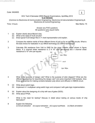
Calculate ON resistance from Vdd to GND for the given inverter circuit shown in figure
below. If p channel sheet resistance is 2 X 10⁴ ohm per-square and n channel sheet
resistance is 104 ohm per-square. Vd
O R
pmos
Lpu: Wpu
U WVin
nmos
vout
Lpu: Wpu
N T
J
4 What is the purpose of design rule? What is the purpose of stick diagram? What are the
different approaches for describing the design rule? List some important CAD toolsets. Give
three approaches for making contacts between poly silicon and diffusion in NMOS circuit.
5 (a) Write about switch logic.
(b) Implement 4:1 multiplexer using switch logic and compare it with gate logic implementation.
6 (a) Explain about the designing of a chip with sea of gates (SOG).
(b) Write about FPGA.
7 What is the need for testing? Discuss in detail about testing at various levels of chip
fabrication?
8 Explain the following:
(i) Circuit extraction (ii) Layout extraction (iii) Layout synthesis (iv) Back annotation
*****
www.jntuworld.com
2. www.jntuworld.com www.jwjobs.net
Code: 9A04605 2
III B. Tech II Semester (R09) Regular Examinations, April/May 2012
VLSI DESIGN
(Common to Electronics & Communication Engineering, Electronics & Instrumentation Engineering &
Electronics & Control Engineering)
Time: 3 hours Max Marks: 70
Answer any FIVE questions
All questions carry equal marks
*****
1 Explain about: (a) ASIC (b) FPGA
(c) CMOS technology (d) Bi CMOS technology.
2 Calculate the threshold voltage of a transistor at zero source/substrate bias. Transistor
has the following parameters.
xox=200oA;Єox=3.5*10-13;øs=0.6V;Qf=1.6*10-8;Єsi=1*10-12;
NA=1015cm-3; Nap=1019cm-3; NII=1*1012.
L D
3
4
5
R
Explain about the constraints in choice of layers.
O
Sketch the stick diagram and lay out for a CMOS gate computing y=(A+B+C+D)/ *D.
Write about design for testability. And hence discuss in detail about the need for it in
6 (a)
VLSI.
U W
‘Implement an 8-bit comparator using 4-bit comparators’ and other interfacing
requirements.
T
(b) With the help of logic diagram explain the working of 4-bit comparator.
N
7 (a) What is meant by logic optimization?
(b) Write about technology dependent and technology independent logic optimization.
8
J
With the help of neat diagrams showing the structure of Antifuse and Vialink explain the
working principle of both as programmable interconnect elements.
*****
www.jntuworld.com
3. www.jntuworld.com www.jwjobs.net
Code: 9A04605 3
III B. Tech II Semester (R09) Regular Examinations, April/May 2012
VLSI DESIGN
(Common to Electronics & Communication Engineering, Electronics & Instrumentation Engineering &
Electronics & Control Engineering)
Time: 3 hours Max Marks: 70
Answer any FIVE questions
All questions carry equal marks
*****
1 Mention different non ideal I-V effects and clearly explain about them.
2 Estimate the total delay when a larger load capacitance is driven by a large inverter
gate N which is driven by a small gate N-1 and so on.
3
4 (a)
With neat sketches explain oxidation process in IC fabrication.
L D
What are design rules? Why is metal-metal spacing larger than poly-poly spacing?
5
(b)
(a)
(b) R
What is stick diagram? Draw the stick diagram and layout for a CMOS inverter.
O
Explain about IDDQ (VDD Supply Current Quiescent) testing for bridging faults.
Explain how a Pseudo random sequence generator and a signature analyzer is used to
test an 8-input combinational circuit.
6 (a)
(b)
W
Implement a full adder circuit using transmission gates.
U
Construct an 8-bit carry select adder using adders and multiplexers.
7 (a)
(b)
T
What are design capture and design verification tools?
With the help of an example using VHDL as both design capture and design verification
N
tool explain the difference between them.
8
J
Summarize the advantages and disadvantages of various design options used to
implement a CMOS system design. Give an example for each.
*****
www.jntuworld.com
4. www.jntuworld.com www.jwjobs.net
Code: 9A04605 4
III B. Tech II Semester (R09) Regular Examinations, April/May 2012
VLSI DESIGN
(Common to Electronics & Communication Engineering, Electronics & Instrumentation Engineering &
Electronics & Control Engineering)
Time: 3 hours Max Marks: 70
Answer any FIVE questions
All questions carry equal marks
*****
1 What are programmable gate arrays? With an architectural diagram explain the working
of gate arrays in the process of implementing a function/system.
2 What is meant by simulation? Explain in detail about switch level and circuit level
3 (a)
(b)
simulation.
L D
With respect to struck at fault model explain about fault collapsing.
For a full adder circuit implemented with XOR and AND gates generate the test vectors
4 (a)
(b)
for SA0 faults on all primary inputs.
O R
With the help of a diagram explain the working of serial/parallel multiplier.
Enumerate the working of a ROM implemented using pseudo NMOS NOR array.
5
6
(a)
(b)
W
What are the advantages of CMOS technology?
Draw the flow chart for VLSI design flow and explain clearly about each step.
U
Explain clearly about different operating regions in nmos transistor with neat diagrams.
7
T
What is the problem of driving large capacitance load? Explain a method to drive such
load.
N
J
8 Explain clearly about the limitations of scaling.
*****
www.jntuworld.com