Semiconductor Front End Manufacturing
•
0 likes•7 views

The semiconductor front end manufacturing process includes metal disposition, in which metal atoms are projected onto the silicon surface to produce a thin metal layer.

Recommended
More Related Content
Similar to Semiconductor Front End Manufacturing
Similar to Semiconductor Front End Manufacturing (20)
More from kensington labs
More from kensington labs (20)
Recently uploaded
Recently uploaded (20)
Semiconductor Front End Manufacturing
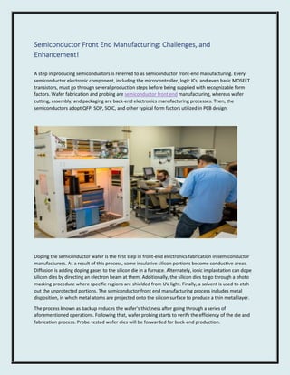
- 1. Semiconductor Front End Manufacturing: Challenges, and Enhancement! A step in producing semiconductors is referred to as semiconductor front-end manufacturing. Every semiconductor electronic component, including the microcontroller, logic ICs, and even basic MOSFET transistors, must go through several production steps before being supplied with recognizable form factors. Wafer fabrication and probing are semiconductor front end manufacturing, whereas wafer cutting, assembly, and packaging are back-end electronics manufacturing processes. Then, the semiconductors adopt QFP, SOP, SOIC, and other typical form factors utilized in PCB design. Doping the semiconductor wafer is the first step in front-end electronics fabrication in semiconductor manufacturers. As a result of this process, some insulative silicon portions become conductive areas. Diffusion is adding doping gases to the silicon die in a furnace. Alternately, ionic implantation can dope silicon dies by directing an electron beam at them. Additionally, the silicon dies to go through a photo masking procedure where specific regions are shielded from UV light. Finally, a solvent is used to etch out the unprotected portions. The semiconductor front end manufacturing process includes metal disposition, in which metal atoms are projected onto the silicon surface to produce a thin metal layer. The process known as backup reduces the wafer's thickness after going through a series of aforementioned operations. Following that, wafer probing starts to verify the efficiency of the die and fabrication process. Probe-tested wafer dies will be forwarded for back-end production.
- 2. Challenges in Semiconductor Front-end Manufacturing Manufacturing semiconductors is a complex task. Manufacturers must overcome obstacles to deliver functional silicon wafers. A photo masking room has much better air quality than an operating room. Any quantity of 0.5-micron particles in a cubic foot of air is judged unacceptable for use in manufacturing. Static charges are another problem in front-end electronics fabrication. Charges in the form of ESD may contaminate the die by attracting surrounding foreign particles. ESD may harm the wafer before, during, or after front-end production. Such occurrences will lower manufacturing yield. Since front-end procedures are typically slower than back-end processes, logistical challenges also influence manufacturers. It will result in inventory planning challenges and may take forward to excesses. Enhancement in Semiconductor Front-end Manufacturing Manufacturers place a high value on yield, and numerous measures have been explored to boost front- end manufacturing productivity. Industry 4.0's introduction of IoT, which makes use of data, has made it possible for manufacturers to identify process line issues more accurately. Manufacturers may better control analytics and yield improvement by adding sensors for various factors at various production points. Wafer contamination has decreased as a result of better air circulation systems installed and the use of machines to limit human involvement. The challenges of reducing semiconductors must also be considered by IC designers because things like signal integrity, smaller nodes, and leakage may have an impact on the manufacturing process. Kensington Laboratories offer the best semiconductor automation solutions, such as Kensington controller, wafer handling robots, wafer pre-aligners, etc. Talk to us and our team of specialists if you want to learn more about how Kensington Laboratories may help you.