
Recommended
Recommended
More Related Content
Similar to How to check pcb production information
Similar to How to check pcb production information (20)
Recently uploaded
Recently uploaded (20)
How to check pcb production information
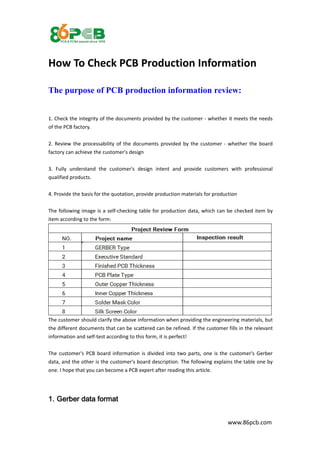
- 1. www.86pcb.com How To Check PCB Production Information The purpose of PCB production information review: 1. Check the integrity of the documents provided by the customer - whether it meets the needs of the PCB factory. 2. Review the processability of the documents provided by the customer - whether the board factory can achieve the customer's design 3. Fully understand the customer's design intent and provide customers with professional qualified products. 4. Provide the basis for the quotation, provide production materials for production The following image is a self-checking table for production data, which can be checked item by item according to the form: The customer should clarify the above information when providing the engineering materials, but the different documents that can be scattered can be refined. If the customer fills in the relevant information and self-test according to this form, it is perfect! The customer's PCB board information is divided into two parts, one is the customer's Gerber data, and the other is the customer's board description. The following explains the table one by one. I hope that you can become a PCB expert after reading this article. 1. Gerber data format
- 2. www.86pcb.com There are many PCB file formats, such as: PROTEL, ALTIUM DESIGNER, CADENCE, EAGLE, ORCAD, PADS, P-CAD and other formats. PCB designers use professional electronic design automation (EDA) or computer-aided design systems (CAD) software. However, the PCB format cannot be directly taken to the factory for production. The PCB production plant needs to convert these PCB format files into gerber format and import them into computer-aided manufacturing software (CAM) for engineering review. The Gerber file is a collection of document formats used by the circuit board industry to describe the image of circuit boards (circuit layers, solder masks, character layers, etc.) and drill and mill data. It is the standard format for image conversion in the printed circuit board industry. File conversion is a key step in the pcb board. It is recommended that customers provide gerber-style files directly. The RS274-X format is optimal, and it is not easy to make mistakes when importing CAM software. At present, the most commonly used CAM software in China is CAM350 and GENESIS2000 software. 2. Implementation Standards Common standards for the PCB industry are as follows: 1.IPC-FC-240 - Flexible Printed Circuit Board Specification 2.IPC-A-600 - Acceptability of printed circuit boards 3.IPC-D-300 - Dimensions and tolerances of printed circuits board 4. IPC-SM-840 - Qualification and performance testing of permanent solder masks on printed circuit boards 5. IPC-6011 - Overview PCB Board Performance Specification 6. IPC-6012 - Rigid PCB Qualification and Performance Verification Specification 3. PCB Thickness The thickness of the finished PCB board must be clear. The circuit board factory will select different plates or laminates to meet the thickness of the finished board according to the number of layers and whether there is characteristic impedance. 4. Plate Type
- 3. www.86pcb.com Commonly used plates are classified as follows from the bottom to the top according to the grade: 94HB/CEM-1/CEM-3/FR-4 The details are as follows: 94HB: ordinary cardboard, not fireproof (minimum material, die punching, can not be used as power board) CEM-1: Single-sided fiberglass board (must be drilled by computer, not die-punched) CEM-3: double-sided semi-fiberglass board (besides double-sided cardboard, which is the lowest material of the double-panel, simple double-panel can use this material) FR-4: double-sided fiberglass board (The classification of flame retardant properties can be divided into 94V-0 /V-1 /V-2, 94-HB four) Prepreg thickness: 1080=2.8mil, 2116=4.5mil, 7628=7mil 5.6. Outer Inner Copper Thickness According to the function that the design engineer wants to achieve in combination with the PCB production process, to clearly the thickness of the inner and outer copper. 1 OZ (ounces) = 35um (microns) = 1.4 mil (mil) 7.8. Solder Mask ColorSilk Screen Color According to the color required by the design engineer, select different surface processes, difficulties and different types to produce. Next Detailed Checking 1. First confirm the number of layers, and whether the layers related to the board are complete. 2. Analyze the minimum line width, line spacing, PAD size, PAD to PAD, line to PAD spacing of the circuit layer to check if they meet the process requirements.
- 4. www.86pcb.com 3. Analyze the minimum aperture, number, and type of holes in the borehole layer, whether there are heavy holes or slots. If there is a hole, the code map needs to be compared with the hole layer. 4. For the solder mask inspection, the solder mask opening layer and the patch layer are simultaneously opened to check whether there is a missing window opening, whether the hole needs to be filled, whether there is insufficient spacing and the need to retain the soldering bridge. If the gap is not possible, if the gap between the solder mask gaps is insufficient, whether to accept the leak line, you need to communicate with the customer to confirm. 5. For the silk screen layer, whether the minimum line width, word width, and word height meet the requirements of the process capability, and whether the space is insufficient can accept the character defect. If there is a part number, it is necessary to verify whether it is consistent with the document. If there is a contradiction, it needs to communicate with the customer to confirm. 6. For the mechanical frame layer, check if there are any non-coincident parts. If there is such a situation, you need to confirm which line is the molding reference. If there is a shape picture, you need to check if the drawing and the mechanical frame layer match. This layer is different for milling or grooving, check whether the copper spacing is satisfied. The customer needs to choose between copper cutting and copper. The above is the PCB production material checking process, hope it will help you.