Study and Comparison of Open Source and Licensed VLSI CAD Tools using CMOS Design Methodology

the design of VLSI circuits can be achieved at many different refinement levels from the most detailed layout to the most abstract architectures. VLSI design has been the study of electronic design automation and related semiconductor science, and many software tools have been written to solve one or more problems associated with the VLSI design flow. VLSI CAD tools have emerged as a boon in assisting VLSI Design engineers to choose and optimize various design models and technology. The importance of CAD tool can be understood by seeing its complex algorithms, data structures and modeling assumptions used in each of the following steps namely logic synthesis, logic verification, layout synthesis, timing verification and many others. Thus a number of standard tools have emerged to design and analyze VLSI chip from one step of the flow to another. Computer-aided design (CAD) is the use of computer systems to assist in the creation, modification, analysis, or optimization of a design. Computer aids in VLSI now offer advance capabilities so engineers can better visualize their product designs. The VLSI CAD tools work sideways together with chip designers to design and analyze entire semiconductor chips. In this paper, a number of open-source and licensed CAD tools will be studied and compared. The tools have been used for various commercial and academic purposes in various companies and universities at different design abstraction levels. This paper will help to comprehend many EDA tools and help to select appropriate computer aid for chip design.
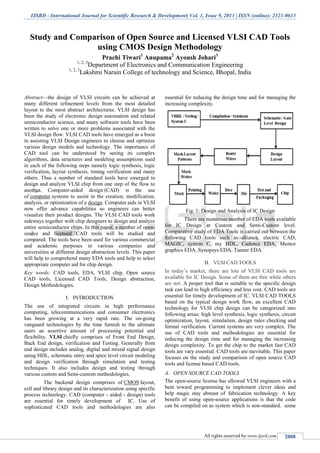
![Study and Comparison of Open Source and Licensed VLSI CAD Tools using CMOS Design Methodology
(IJSRD/Vol. 1/Issue 9/2013/0079)
All rights reserved by www.ijsrd.com 2009
open source VLSI cad tools are selected for general
introduction and comparison.
Fig. 2: Simple VLSI CAD tool chain
Tools
Function and
Type
Platform
Latest
Version
Description
Alliance
Logic to Layout,
Mixed signal
Linux Version 5.0
Set of free
CAD tools
and
portable
libraries. It
supports
the
standard
VLSI
description
formats
like
SPICE,
EDIF,
VHDL,
CIF and
GDS2.
Magic
Circuit Layout,
Mixed signal
Linux Version 7.5
Easiest
tool to use
for circuit
layout,
contain an
incrementa
l design-
rule
checker
Electric
Logic to Layout,
Mixed signal
Linux,
Windo
ws and
Macint
osh
Version 9.04
It is a
sophisticat
ed
electrical
CAD
system
that can
handle
many
forms of
circuit
design.
My
HDL
Hardware
description
language,
Electronic
system level
Linux Version 0.8
MyHDL is
to use
Python
generators
to model
the
concurrenc
y required
in
hardware.
System
C
Library For
digital design,
Electronic
system level
Linux Version 2.2
System C
is C++
based
system
level
description
language.
Ngspice
Circuit
simulator,
Mixed signal
Linux Version 25
It
implement
s three
classes of
analysis
Nonlinear
DC
analyses,
Nonlinear
Transient
analyses
and Linear
AC
analyses.
Table. 1: Comparative study of various open sources VLSI
CAD tools[6,25,26,27]
LICENSED VLSI CAD TOOLSB.
Electronic Design Automation (EDA) products by various
vendors are sold on the basis of licensing models. EDA
licensing traditionally follows a perpetual model, in which
users buy a tool license that essentially lasts forever.
Along with that perpetual license, vendors typically
sell a maintenance deal on an annual basis.
Tools
Function
and Type
Platform
Latest
Version
Description
Cadence EDA
Comple
te CAD
flow,
Analog
and
mixed
signal
Unix and pc-
based
systems
version 16.6
Cadence
provides
contracted
methodology
and design
services. as well
as silicon design
IP.
Mentor graphics
EDA
Comple
te CAD
flow,
Analog
and
mixed
signal
Linux Genivi 3.0
The Mentor
Graphics tool is
Design
Manager, tool
that is
specifically
designed to
preserve and
manipulate the
objects.
Synopsys
EDA
Comple
te CAD
flow,
Analog
and
mixed
signal
Linux
Virtualizer
13.06
Synopsys is a
world leader in
software and IP
for
semiconductor
design,
verification.](data:image/gif;base64,R0lGODlhAQABAIAAAAAAAP///yH5BAEAAAAALAAAAAABAAEAAAIBRAA7)
Recommended
Recommended
More Related Content
What's hot
Similar to Study and Comparison of Open Source and Licensed VLSI CAD Tools using CMOS Design Methodology
Similar to Study and Comparison of Open Source and Licensed VLSI CAD Tools using CMOS Design Methodology (20)
More from ijsrd.com
More from ijsrd.com (20)
Recently uploaded
Recently uploaded (20)
Study and Comparison of Open Source and Licensed VLSI CAD Tools using CMOS Design Methodology
- 1. IJSRD - International Journal for Scientific Research & Development| Vol. 1, Issue 9, 2013 | ISSN (online): 2321-0613 All rights reserved by www.ijsrd.com 2008 Study and Comparison of Open Source and Licensed VLSI CAD Tools using CMOS Design Methodology Prachi Tiwari1 Anupama2 Ayoush Johari3 1, 2, 3 Department of Electronics and Communication Engineering 1, 2, 3 Lakshmi Narain College of technology and Science, Bhopal, India Abstract—the design of VLSI circuits can be achieved at many different refinement levels from the most detailed layout to the most abstract architectures. VLSI design has been the study of electronic design automation and related semiconductor science, and many software tools have been written to solve one or more problems associated with the VLSI design flow. VLSI CAD tools have emerged as a boon in assisting VLSI Design engineers to choose and optimize various design models and technology. The importance of CAD tool can be understood by seeing its complex algorithms, data structures and modeling assumptions used in each of the following steps namely logic synthesis, logic verification, layout synthesis, timing verification and many others. Thus a number of standard tools have emerged to design and analyze VLSI chip from one step of the flow to another. Computer-aided design (CAD) is the use of computer systems to assist in the creation, modification, analysis, or optimization of a design. Computer aids in VLSI now offer advance capabilities so engineers can better visualize their product designs. The VLSI CAD tools work sideways together with chip designers to design and analyze entire semiconductor chips. In this paper, a number of open- source and licensed CAD tools will be studied and compared. The tools have been used for various commercial and academic purposes in various companies and universities at different design abstraction levels. This paper will help to comprehend many EDA tools and help to select appropriate computer aid for chip design. Key words: CAD tools, EDA, VLSI chip, Open source CAD tools, Licensed CAD Tools, Design abstraction, Design Methodologies. I. INTRODUCTION The use of integrated circuits in high performance computing, telecommunications and consumer electronics has been growing at a very rapid rate. The on-going vanguard technologies by the time furnish to the ultimate users an assertive amount of processing potential and flexibility. VLSI chiefly comprises of Front End Design, Back End design, verification and Testing. Generally front end design includes analog, digital and mixed signal design using HDL, schematic entry and spice level circuit modeling and design verification through simulation and testing techniques. It also includes design and testing through various custom and Semi-custom methodologies. The backend design comprises of CMOS layout, cell and library design and its characterization using specific process technology. CAD (computer - aided - design) tools are essential for timely development of IC. Use of sophisticated CAD tools and methodologies are also essential for reducing the design time and for managing the increasing complexity. Fig. 1: Design and Analysis of IC Design There are numerous number of EDA tools available for IC Design at Custom and Semi-Custom level. Comparative study of EDA Tools is carried out between the following CAD tools such as:-alliance, electric CAD, MAGIC, system C, my HDL, Cadence EDA, Mentor graphics EDA, Synopsys EDA, Tanner EDA. II. VLSI CAD TOOLS In today’s market, there are lots of VLSI CAD tools are available for IC Design. Some of them are free while others are not. A proper tool that is suitable to the specific design task can lead to high efficiency and less cost. CAD tools are essential for timely development of IC. VLSI CAD TOOLS based on the typical design work flow, an excellent CAD technology for VLSI chip design can be categorized into following areas: high level synthesis, logic synthesis, circuit optimization, layout, simulation, design rules checking and formal verification. Current systems are very complex. The use of CAD tools and methodologies are essential for reducing the design time and for managing the increasing design complexity. To get the chip to the market fast CAD tools are vary essential. CAD tools are inevitable. This paper focuses on the study and comparison of open source CAD tools and license based CAD tools. OPEN SOURCE CAD TOOLSA. The open-source license has allowed VLSI engineers with a bent toward programming to implement clever ideas and help magic stay abreast of fabrication technology. A key benefit of using open-source applications is that the code can be compiled on as system which is non-standard. some
- 2. Study and Comparison of Open Source and Licensed VLSI CAD Tools using CMOS Design Methodology (IJSRD/Vol. 1/Issue 9/2013/0079) All rights reserved by www.ijsrd.com 2009 open source VLSI cad tools are selected for general introduction and comparison. Fig. 2: Simple VLSI CAD tool chain Tools Function and Type Platform Latest Version Description Alliance Logic to Layout, Mixed signal Linux Version 5.0 Set of free CAD tools and portable libraries. It supports the standard VLSI description formats like SPICE, EDIF, VHDL, CIF and GDS2. Magic Circuit Layout, Mixed signal Linux Version 7.5 Easiest tool to use for circuit layout, contain an incrementa l design- rule checker Electric Logic to Layout, Mixed signal Linux, Windo ws and Macint osh Version 9.04 It is a sophisticat ed electrical CAD system that can handle many forms of circuit design. My HDL Hardware description language, Electronic system level Linux Version 0.8 MyHDL is to use Python generators to model the concurrenc y required in hardware. System C Library For digital design, Electronic system level Linux Version 2.2 System C is C++ based system level description language. Ngspice Circuit simulator, Mixed signal Linux Version 25 It implement s three classes of analysis Nonlinear DC analyses, Nonlinear Transient analyses and Linear AC analyses. Table. 1: Comparative study of various open sources VLSI CAD tools[6,25,26,27] LICENSED VLSI CAD TOOLSB. Electronic Design Automation (EDA) products by various vendors are sold on the basis of licensing models. EDA licensing traditionally follows a perpetual model, in which users buy a tool license that essentially lasts forever. Along with that perpetual license, vendors typically sell a maintenance deal on an annual basis. Tools Function and Type Platform Latest Version Description Cadence EDA Comple te CAD flow, Analog and mixed signal Unix and pc- based systems version 16.6 Cadence provides contracted methodology and design services. as well as silicon design IP. Mentor graphics EDA Comple te CAD flow, Analog and mixed signal Linux Genivi 3.0 The Mentor Graphics tool is Design Manager, tool that is specifically designed to preserve and manipulate the objects. Synopsys EDA Comple te CAD flow, Analog and mixed signal Linux Virtualizer 13.06 Synopsys is a world leader in software and IP for semiconductor design, verification.
- 3. Study and Comparison of Open Source and Licensed VLSI CAD Tools using CMOS Design Methodology (IJSRD/Vol. 1/Issue 9/2013/0079) All rights reserved by www.ijsrd.com 2010 Tanner EDA Comple te CAD flow, Analog and mixed signal Windows, Linux. V16 Tanner EDA is a suite of tools for the design of integrated circuits. Tanner EDA is mainly used to analyze circuits at switch level & gate level. Table 2: Comparative study of licensed VLSI EDA tools [ 34,21,20] Designer’s aim is to Transfer Design description in one domain into a fully equivalent design descriptions in respective other. DESIGN METHODOLOGYC. Systematic design methods or the design methodologies are necessary for successfully designing complex digital hardware. Our design methods usually differ by the number of abstraction levels and the complexities involved. Fig. 4: Limitation and challenges to overcome at various abstraction levels in VLSI Design and CAD Fig. 5: Abstraction Hierarchy 1 [1] The design cycle may be short or can be long depends on the requirement of the requirement. Assuring integrity of the design and success requirement are the different parts in characterizing the design. Various methodologies look in to the design with multiple views and the representation will be different with each set of characterization. The complexity can rise further due to insufficient documentation. Fig. 6: Abstraction Hierarchy 2 [1] III. VLSI EDA CLASSIFICATION A kind of activity which uses a computer to assist on the creation, modification and analysis of design. CAD tools generally consist of the following components, input handler (input from mouse or keyboard), data structure and algorithms (in memory), output handler (output to display). CAD environment generally consists of a simulator, design space exploration and design sign off. Following is the brief classification of CAD 1) High Level synthesis CHDL 2) Logic Synthesis Tools 3) Circuit optimization Tools i) Transistor sizing Tools ii) Process variation Tools iii) Statistical Design Tools 4) Layout Tools i) Floor planning Tools ii) Place and Route iii) Module Generation iv) Automatic Call and placement routing 5) Layout Extraction Tools 6) Simulation (SPICE for circuit level simulation) 7) Layout schematic verification Tools Fig. 7: Co-evolution of CAD Tools and methodologies [19] The role of the CAD tool in VLSI design is 1) Accurately generated and easily modifiable graphical representation of the product. The user can nearly view the actual product on screen, make any modifications to it, and present his/her ideas on screen without any prototype, especially during the early stages of the design process. 2) Perform complex design analysis in short time and Implementing Finite Elements. 3) The user can perform the following analysis methods: i) Static, Dynamic and Natural Frequency analysis, Heat transfer analysis, Plastic analysis, Fluid flow analysis, Motion analysis, Tolerance analysis, Design optimization. 4) Record and recall information with consistency and speed. IV. VLSI EDA COMPLEXITIES [1,11] Problem Domain ComplexityA. The functionality of the integrated chip should be taken into account with respect to the 3p’s [9] i.e. price, power and performance. The problem may be competing or posseing
- 4. Study and Comparison of Open Source and Licensed VLSI CAD Tools using CMOS Design Methodology (IJSRD/Vol. 1/Issue 9/2013/0079) All rights reserved by www.ijsrd.com 2011 contradictory requirements in terms of speed power and other design metrics. The problem can also arise due to the mismatch between the users and designers. Application area specialization and knowledge with ever changing and evolving specifications. The cost of design and development also depends on the extent to which the specification issues have been captured. Design/ Development Process ComplexityB. VLSI is a fast growing industry, if automobile industry would have developed at the same rate cars would have been far more affordable. The rapid change in technology is basically due to advancements in various fabrication procedures and simultaneously in design methodologies. The modularity and hierarchical let the large task into smaller modules, the large tasks requiring multidisciplinary team, separated by geographical regions. The design cycle may be short or can be long depends on the requirement of the requirement. Assuring integrity of the design and success requirement are the different parts in characterizing the design. Various methodologies look in to the design with multiple views and the representation will be different with each set of characterization. The complexity can rise further due to insufficient documentation. Complexity of choicesC. As the time goes on, advancement in the design methodologies have been done with respect to speed area and power dissipation. Many technologies and implementation choices such as NMOS, PMOS. Many methodologies (FPGA, Semi-custom, CPLD, Full custom, ASIC etc.). Many different styles of implementation in static (ratioed, general transistor logic, pass transistor logic, transmission gate logic etc.). Many logic styles in dynamic 2 phase,4 phase) Cascaded logic (Domino, NPMOS, Zipper etc.). Many possible partitions at each level increase the complexity of choices.[4,9] Fig. 8: Design representation levels and formats associated [1] Complexities of design tasksD. These complexities include various clocking and timing issues, testing related issues, packaging related issues and concurrency related operations. The design tasks exist in the front end as well as in the back end. V. LIMITATIONS AND CHALLENGES TO BE OVERCOMEIN CAD TOOLS [1, 11] In this section, various established and emerging design quality metrics and the main challenges of CAD tools to effectively predict, analyze their interactions, and optimize them in the CMOS technology were discussed. In the last few years, the research developers have witnessed increasing levels of interactions between physical, logical, and functional realms in the synthesis of VLSI circuit and systems. Various approaches with varying levels of interactions between the synthesis and layout phases have been proposed. These techniques are classified into several classes: Gain-Based SynthesisA. It is based on logical effort theory, which performs the gate sizing based on logical effort, electrical effort and timing constraints. The succeeding layout phase is then performed with additional timing and capacitance constraints to meet the initial gate sizing decision. Appropriate circuit libraries are must. Layout-Friendly SynthesisB. Here, Synthesis of layout implications is given more importance. The wire planning is a best example for this type of synthesis. The research developers use the placement of I/O pins to achieve a layout-friendly logic factorization. Layout-Driven SynthesisC. In this synthesis depends on companion, layout/placement of various parts of the logic. After synthesis nodes may get created or deleted, and the companion layout may need to be updated to reflect these changes. The benefit of having a companion layout view is access to a more realistic estimate about inter-connects parasitic. This would allow the synthesis phase to make better decisions, while optimizing the logic. Integrated Synthesis and LayoutD. The ultimate integration of the synthesis and layout phases was carried out by this class. Synthesis-Driven LayoutE. This category consists of those techniques which perform layout optimization moves either within the synthesis phase or in a post-layout phase where synthesis and layout optimizations are applied to improve the design or meet the performance constraints. Synthesis-Friendly LayoutF. This type of synthesis consists of layout synthesis algorithms and environments which is capable of withstanding functional and logic changes, with minimal disruption to the layout. VI. CONCLUSION With design technology, it would be possible to implement, verify and test the complex integrated circuits. It is through design technology that the ideas and objectives of design, circuit and fabrication engineers are transformed into reality
- 5. Study and Comparison of Open Source and Licensed VLSI CAD Tools using CMOS Design Methodology (IJSRD/Vol. 1/Issue 9/2013/0079) All rights reserved by www.ijsrd.com 2012 and the quality of the design tools and associated methodologies determine the design time, performance, cost and the correctness of the final product chip. The development in the design tools, collaborative design methods, the role of human factors and integration factors in the design technology marks the outline of various design methodologies. This paper explains design quality metrics from a CAD tool perspective. Various shortcomings of the current CAD tools and methodologies to tackle the VLSI design challenges were discussed and several promising remedies and their implications on design and methodologies are explored. Below table will summarize a comparative study of open source and licensed CAD Tools. Key Features Open Source EDA Tool Licensed EDA Tool Design time More Less Performance Good Excellent Correctness Good Excellent Reliability Good Good Compatibility with Operating System Compatible with Linux, windows and others. Compatible with mostly Linux and similar Unix flavors. Design Quality Depends on flow Good Standardization For academic purposes. For academic and commercial purposes. Table. 3: Comparative study of Open source CAD tools and Licensed VLSI EDA tools REFERENCES [1] Randal E. Bryant, Kwang-TingCheng , Andrew B Kahang, Kurt Kreutzer, Wojciech Maly, Richard Newton, Lawerance Pileggi, Jan M Rabaey, Alberto Saniovanni- Vincentelli, “Limitations and Challenges of CAD technology for CMOS VLSI” [2] Catherine H. Gebotys, Mohamed I. Elmasry, “Vlsi Design Synthesis and Testability” [3] A.H. Farrahi, D.J. Hathaway, M.Wang and M.Sarrafzadeh, “Quality OF EDA CAD Tools: Definitions, Metrics and Directions” [4] K.A. Sumithra Devi, “Algorithms for CAD tools VLSI design” [5] Neil Weste and David Harris, CMOS VLSI Design, the Third Edition, Pearson Education, 2004. [6] Static Free Software. November 2009 http://www.staticfreesoft.com. [7] Alliance. November 2009. http://www asim.lip6.fr/recherche/alliance. [8] Magic VLSI Resource. November 2009. http://www.opencircuitdesign.com/magic. [9] Cadence OrCAD Solutions. February 2010. http://www.cadence.com/products/orcad. [10] Yohn K. Ousterhout, Gordon T. Hamachi, Robert N. Mayo, Walter S. Scott, and George S. Taylor, “Magic: A VLSI Layout System”, Design Automation, 1984. 21st Conference on, 25-27 June 1984. [11] Ayoush Johari, VVS Lavanya, Rakeshwari Pal, “Study of VLSI Design Methodologies and Limitations using CAD tools for CMOS Technology” IJEECT, Vol.10, Issue9 ,August 2013, INFLUENCE 2013, Bhopal (ISSN-2229-3207). [12] Scott, W. S. and Ousterhout, J. K. “Plowing: Interactive Stretching and Compaction in Magic”, Design Automation, 1984. [13] Alain Greiner and Francois Pecheux, “ALLIANCE: A complete Set of CAD Tools for teaching VLSI Design”, Technical Report: Laboratoire MASI/CAO- VLSI, Institute de Programmation, University Pierre et Marie, 1992. [14] Amara Amara, Alain Greiner, Luis Lucas, Frederic Petrot, Franck Wajsburt, Laurent Winckel, “The Portable Cell Libraries of the Freeware Alliance CAD system”. [15] IRSIM, February 2010. http://opencircuitdesign.com/irsim. [16] J. B. MacQueen, "Some Methods for classification and Analysis of Multivariate Observations”, Proceedings of 5-th Berkeley Symposium on Mathematical Statistics and Probability, Berkeley, University of California Press, 1967, pp. 281-297. [17] http://nptel.iitm.ac.in/courses/IIT- MADRAS/CAD_for_VLSI_Design_I/index.php [18] Topped – Open Source Layout Editor, February 2010. http://www.toped.org.uk. [19] Computer Aids for VLSI Design Second Edition Steven M. Rubin [20] Synopsys, “Design Compiler FPGA,” 2004. [21] Mentor Graphics, “Leanardo Spectrum,” 2001. [22] V. Betz, J. Rose, and A. Marquardt, Architecture and CAD for Deep-Submicron FPGAs.Kluwer Academic Publishers, 1999. [23] Bar, M., Fogel, K., Open Source Development with CVS, 3rd Edition, Para glyph Press, 2003. Chromatic, Myths Open Source Developers Tell Ourselves, O’Reilly On Lamp, [24] Fellor J, Fitzgerald B., Raymond, E., Understanding Open Source Software Development, Addison- Wesley,2001, ISBN 0201734966 [25] Alliance. http://www.asim.lip6.fr/recheche/alliance [26] Magic VLSI Resource. http://www.opencircuitdesign.com/magic [27] http://www.vlsiacademy.org/open-source-cad- tools.html [28] Custom IC Design, http://www.cadence.com/products/cic [29] D. Lidsky, J. M. Rabaey, “Early Power Exploration--a World Wide Web Application”, Design Automation Conference, June 1996. [30] M. Nemani and F. Najm. “High-Level Area and Power Estimation for VLSI, Circuits”. IEEE Transactions on Computer Aided Design, 18(6):697–713, June 1999. [31] C. S. Shung et al., “An integrated CAD system for algorithmspecificIC design,” IEEE Trans. CAD Integ. Circ. and Syst., Apr.1999 [32] Alain Greiner and Francois Pecheux, “ALLIANCE: A complete Set of CAD Tools for teaching VLSI Design”, Technical Report: Laboratoire MASI/CAO-
- 6. Study and Comparison of Open Source and Licensed VLSI CAD Tools using CMOS Design Methodology (IJSRD/Vol. 1/Issue 9/2013/0079) All rights reserved by www.ijsrd.com 2013 VLSI, Institut de Programmation, Universite Pierre et Marie, 1992. [33] Amara Amara, Alain Greiner, Luis Lucas, Frederic Petrot, Franck Wajsburt, Laurent Winckel, “The Portable Cell Libraries of the Freeware Alliance CAD system”. [34] Cadence OrCAD Solutions. February 2010. http://www.cadence.com/products/orcad. [35] Magic VLSI Resource. November 2009. http://www.opencircuitdesign.com/magic.