

Recommended
More Related Content
What's hot
What's hot (20)
Viewers also liked
Viewers also liked (13)
Recently uploaded
Recently uploaded (20)
77
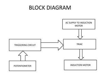
- 1. BLOCK DIAGRAM TRIGGERING CIRCUIT POTENTIOMETER AC SUPPLY TO INDUCTION MOTOR TRIAC INDUCTION MOTOR
- 7. OP-AMP 741COMPARATOR AND CONNECTION MADE TO IT Vcc vcc 6 1 0 h ing Input to AND gate R4 1kohm 741 7 1 6 U1 4 0
- 8. PIN DIAGRAM OF LM 741 1 2 3 4 8 7 6 5 Offset null Inverting input Non inverting null V- NC V+ Output Offset null
- 10. PIN DIAGRAM OF 555 TIMER 8 7 6 5 1 2 3 4 Ground Trigger Output Reset Discharge Vcc Threshold Control voltage 8- PIN DIP
- 12. OUTPUT OF 555 TIMER Amplitude PERIOD
- 13. AND GATE AND ITS TRURH TABLE:- A 0 0 1 1 B 0 1 0 1 OUTPUT 0 0 0 1 INPUT A INPUT B OUTPUT
- 17. PROGRESS OF THE PROJECT The simulation of the schematic circuit in the multisim software have been done.
- 18. THANK YOU