Python Notes for mca i year students osmania university.docx
Lab module sem
1. EXPERIMENT 1:
Microstructural Analysis Using Scanning Electron Microscope (SEM)
1.0 OBJECTIVES
1.1 To apply the theory of materials characterization technique using SEM-EDX
1.2 To investigate the microstructural properties of all material types including
ceramic, metal and polymer
2.0 INTRODUCTION
The SEM has a large depth of field, which allows a large amount of the sample to be in
focus at one time. Scanning Electron Microscope (SEM) is a microscope that using electrons
rather than light to form magnified and detailed 3-dimensional images at much high
magnifications ranging from 10x to 50 000x could be possible. The combination of higher
magnification, larger depth of focus, greater resolution, and ease of sample observation makes
the SEM one of the most characterization instruments used in research areas today.
The surface of a specimen to examine may or may not be polished and etched but it must be
electrically conductive. Because of that, a very thin metallic surface coating must be applied for
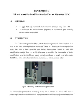
Figure 1: Scanning electron microscope machine
2. nonconductive specimen includes gold, aluminum or carbon using sputter coater as shown in
Figure 1.2.
Scanning Electron Microscope (SEM) uses electrons beam which comes from various types of
filament for example Tungsten hairpin gun. This filament is a loop of tungsten which functions
as the cathode. Other examples of filaments are Lanthanum Hexaboride filaments and field
emission (FE) guns. The surface of a specimen to be examined is scanned with an electron beam
and the reflected (or back scattered) beam of electron is collected then displayed on a cathode ray
tube. The images created without light waves are rendered black and white
Secondary Electron Imaging shows the topography of surface features a few nm across
produce adequate contrast images. Materials are viewed at useful magnifications up to 50
000x without damaging the sample
Backscattered Electron Imaging shows the spatial distribution of elements or compounds
within the top micron of the sample. Features as small as 10 nm are resolved and
composition variations of as little as as 0.2% determined.
Data Output is generated and display on the Cathode Ray Tube (CRT) monitor and the
image represent surface features of the specimen. To determine the chemical composition
of a microscopic area of a solid sample, the Energy Dispersive Analysis (EDA) or Energy
Dispersive X-ray (EDX) is used.
Figure 1.2: Sputter coater
3. This equipment can be used for a wide range of elements on a multitude of samples, such as
polished surfaces, fracture surfaces, powders, and surface films.
3.0 EXPERIMENTAL PROCEDURE
3.1 Different specimens of metal, ceramic and polymer will be provided to
investigate. Prepare fracture and polish surface to observe surface microstructure.
3.2 Apply various magnifications, from low to high magnification to visualize an in-
depth microstructure for both fracture and polished surface.
3.3 Observe and record other micro defects occurred, also the porosity and the
uniformity of pores.
3.4 From micrographs result, draw microstructure and calculate the grain size
distribution of each specimen.
3.5 EDX technique will be use to identify chemical element of specimens.
3.6 From EDX investigation, determine the bulk chemical composition of specimens
as well as the micro-chemical composition of contaminants.
4.0 RESULTS AND DISCUSSION
Analyse microstructure features from micrograph result including homogeneity, grain size
distribution, porosity and significance of pore location in grain boundaries, trapped pores, etc.
From EDX analysis, state the major element specimen. For minor element (if coexist), state what
it is and explain why it exist together with the major element.
Explain the relationship of the porosity towards the strength of material. Based on the analysis
results and the information obtained from references, what are the possible causes of the defects
occur. Recommend any possible corrective and preventative actions for these defects.
4. REFERENCES
[1] Callister, W. D. (2005). Fundamentals of Materials Science and Engineering. 2nd
Edition. John Wiley & Sons, United States of America.
[2] Callister, W. D. (2003). Materials Science and Engineering an Introduction.62nd
Edition. John Wiley & Sons, United States of America.
[3] Clarke A. R. and Eberhardt C. N. (2002). Microscopy Techniques for Materials
Science. CRC Press, New York.
[4] Santos C. et al. (2003). The Importance of Si3Ni4 Characterization by SEM at the
Different Sintering Stages. Acta Microscopia. 12(1), 83-86.
[5] Costa C. E. et al. (2003). Characterization of Casting Iron Powder from Recycled
Swarf. Journal of Material Processing Technology. (143-144). 138-143.
[6] Henkel, D. & Pense, A. W. (2001). Structure and Properties of Engineering
Materials. 5th
Edition. McGraw Hill International, Singapore.
[7] Polmear, I. J. (1981). Light Alloys- Metallurgy of the Light Metals. Edward Arnold,
Great Britain.