1. Abstract
Analytical Method
Once data has been collected for a sample, it is analyzed using the
modeling program SIMNRA. After a model that accurately simulates the
data is constructed, the results are compiled to illustrate what was learned.
These reports, which are sent to our colleagues in India, focus on five main
areas of interest: elements found in both the thin film and the substrate,
unexpected elements, substrate roughness, film homogeneity and our
conclusions.
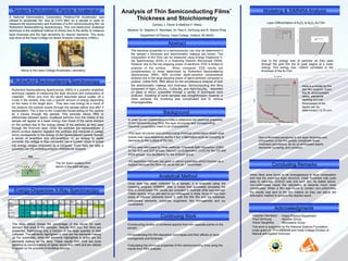
Tandem Electrostatic Particle Accelerator
A National Electrostatics Corporation PelletronTM Accelerator was
utilized to accelerate He+ ions at 2.975 MeV on a sample in order to
measure the stoichiometry and thickness of a thin semiconducting film via
Rutherford Backscattering Spectroscopy. This non-destructive analytical
technique is the analytical method of choice due to the ability to measure
layer thickness and the high sensitivity for heavier elements. This study
was done at the Hope College Ion Beam Analysis Laboratory (HIBAL).
Above is the Hope College Accelerator Laboratory
Rutherford Backscattering Spectroscopy
Rutherford Backscattering Spectroscopy (RBS) is a powerful analytical
technique capable of measuring the layer structure and composition of
materials. When ions from the beam described above scatter off a
nuclei in the sample, they lose a specific amount of energy depending
on the mass of the target atom. They also lose energy as a result of
the distance the particle travels through the sample before and after if
backscatters. This is due to the Coulombic forces acting on the particle
as it travels through the sample. This principle allows RBS to
differentiate between layers. Scattered particles from the middle of the
sample will appear at a lower energy than those of the same element
on the surface due to the energy losses of the particles as they pass
through the foremost layer. Once the particles are backscattered, a
silicon surface detector registers the particles and transmits a voltage
which corresponds to the energy of the backscattered particle through
a series of amplifiers and pre-amplifiers. In an analog to digital
converter the voltage is then converted into a number which is sorted
into energy ranges (channels) by a computer. From here the data is
uploaded into the modeling program SIMNRA for analysis.
The ion beam scatters from
atoms in the solid sample..
Continuing Work
• Constructing models of combined spectra from two separate points on the
sample.
• Understanding thin film deposition techniques and their effects on layer
homogeneity and thickness.
• Calculating the electrical properties of thin semiconducting films using the
results from RBS analysis.
Acknowledgments
Analysis of Thin Semiconducting Films’
Thickness and Stoichiometry
Zachary J. Diener & Matthew P. Weiss
Mentors: Dr. Stephen K. Remillard, Dr. Paul A. DeYoung and R. Reena Philip
Department of Physics, Hope College, Holland, MI 49423
Energy-Dispersive X-Ray Spectroscopy
Background
Modeling & SIMNRA Analysis
Concluding Remarks
In order for our collaborators in India to determine the electrical properties
of thin semiconducting films, the layer structures and corresponding
chemical composition need to be characterized.
• The layer structures and corresponding chemical composition reveal what
events may have happened during a film’s fabrication such as clumping of
elements on the surface of the film.
• Films were fabricated by three methods: Chemical Bath Deposition (CBD)
for the SnS and ZnO groups, Vacuum Co-Evaporation (VCE) for the GS and
AIGS groups, and Sputtering for the (InSn)O group.
• All deposition methods use glass or silicon substrates which function as a
support because the films can be as thin as 1 micrometer.
The electrical properties of a semiconductor can only be determined if
the sample’s thickness and stoichiometric makeup are known. The
composition of thin films can be measured using Energy Dispersive X-
ray Spectroscopy (EDS) in a Scanning Electron Microscope (SEM).
However due to the low stopping power of electrons, EDS is limited to
analysis of the surface. When compared, EDS results are
complementary to those determined by Rutherford Backscattering
Spectroscopy (RBS). RBS provides depth-sensitive compositional
analysis due to the large stopping power of alpha particles compared to
protons. Unlike EDS, RBS allows for the simultaneous analysis of both
the stoichiometric makeup and thickness. Semiconducting thin films
composed of AgIn1-xGaxSe2, CuGaxSe2 and Ag(InGa)5Se8 deposited
on glass or silicon substrates through a variety of techniques were
analyzed. Modeling of some samples was straightforward; however in
other samples the modeling was complicated due to various
inhomogeneities.
Layer Differentiation of Al2O3 & Al2O3 Au Film
Due to the energy loss of particles as they pass
through the gold film the Al peak begins at a lower
energy. This energy loss ~25KeV correlates to the
thickness of the Au Film
Original energy of Al
peak
Here is a model for the
thin film (InSn)O. From
this fit, stoichiometric
ratios, elemental
layering and the
thicknesses of the
layers can be
determined (~3.74 µm)
The table above shows the percentage of the atoms for each
element that exist in the samples. Results from four thin films are
presented, highlighting only a fraction of the large quantity of data
collected. The elements highlighted in blue are the elements making
up the substrates, while the elements highlighted in green are the
elements making up the films. These results from EDS are more
sensitive to concentrations of lighter atoms than RBS and are utilized
to speed up the process of modeling spectra.
Non-uniformities pertaining to the layer thickness and
composition of the film greatly complicate linear
thickness calculations, as do un-anticipated layers,
elemental clumping, and oxidation.
• Stephen Remillard
• Paul DeYoung
• Dave Daughtrey
This work is supported by the National Science Foundation
under grant no. PHY-0969058 and Hope College Division of
Natural and Applied Sciences.
• Hope Physics Department
• Nuclear Group
• Microwave Group
When films were found to be homogeneous in layer composition
and had the expected layer structure, linear thickness was quite
easy to calculate. (InSn)O was one such film. As stated above,
non-uniformities cause the calculation to become much more
complicated. When a film was found to contain non-uniformities
the results was sent to the film makers so they can adjust the
fabrication method to achieve the desired result.
Film O Si Na Ca Mg Al K Ag In
Sn
(Tin) Ga Se Cu Sr Zn
ZnOSr 55.53 22.81 9.86 2.58 1.75 0.61 0.78 --- --- --- --- --- --- 0.17 5.91
GaS 53.4 25.37 8.77 2.85 1.88 0.71 0.71 --- --- --- 6.23 0.09 --- --- ---
AIGS III 3.94 86.6 --- --- --- --- --- 1.41 1.26 --- 4.28 2.51 --- --- ---
(InSn)O 60.26 10.19 1.31 1.5 0.8 0.54 --- --- 22.21 3.18 --- --- --- --- ---