chaitra-1.pptx fake news detection using machine learning
Announcement_webinar_DOES-EDS_EMERGING DEVICES, CIRCUITS AND SYSTEMS.pdf
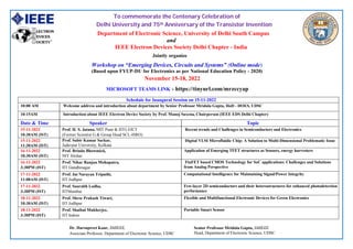
1. To commemorate the Centenary Celebration of
Delhi University and 75th Anniversary of the Transistor Invention
Department of Electronic Science, University of Delhi South Campus
and
IEEE Electron Devices Society Delhi Chapter - India
Jointly organize
Workshop on “Emerging Devices, Circuits and Systems” (Online mode)
(Based upon FYUP-DU for Electronics as per National Education Policy - 2020)
November 15-18, 2022
MICROSOFT TEAMS LINK - https://tinyurl.com/mrzccyap
Schedule for Inaugural Session on 15-11-2022
10:00 AM Welcome address and introduction about department by Senior Professor Mridula Gupta, HoD - DOES, UDSC
10:15AM Introduction about IEEE Electron Device Society by Prof. Manoj Saxena, Chairperson (IEEE EDS Delhi Chapter)
Date & Time Speaker Topic
15-11-2022
10:30AM (IST)
Prof. H. S. Jatana, MIT Pune & IITG EICT
(Former Scientist G & Group Head SCL-ISRO)
Recent trends and Challenges in Semiconductors and Electronics
15-11-2022
11:30AM (IST)
Prof. Subir Kumar Sarkar,
Jadavpur University, Kolkata
Digital VLSI Microfluidic Chip: A Solution to Multi-Dimensional Problematic Issue
16-11-2022
10:30AM (IST)
Prof. Brinda Bhowmick,
NIT Silchar
Application of Emerging TFET structures as Sensors, energy harvesters
16-11-2022
3:30PM (IST)
Prof. Nihar Ranjan Mohapatra,
IIT Gandhinagar
FinFET based CMOS Technology for SoC applications: Challenges and Solutions
from Analog Perspective
17-11-2022
11:00AM (IST)
Prof. Jai Narayan Tripathi,
IIT Jodhpur
Computational Intelligence for Maintaining Signal/Power Integrity
17-11-2022
3:30PM (IST)
Prof. Saurabh Lodha,
IITMumbai
Few-layer 2D semiconductors and their heterostructures for enhanced photodetection
performance
18-11-2022
10:30AM (IST)
Prof. Shree Prakash Tiwari,
IIT Jodhpur
Flexible and Multifunctional Electronic Devices for Green Electronics
18-11-2022
3:30PM (IST)
Prof. Shaibal Mukherjee,
IIT Indore
Portable Smart Sensor
Dr. Harsupreet Kaur, SMIEEE,
Associate Professor, Department of Electronic Science, UDSC
Senior Professor Mridula Gupta, SMIEEE
Head, Department of Electronic Science, UDSC
2. November 15, 2022, 10:30 AM (IST)
Recent trends and Challenges in Semiconductors and Electronics
Prof. H. S. Jatana
MIT Pune & IITG EICT
(Former Scientist G & Group Head SCL-ISRO)
Abstract - The talk covers wide spectrum of semiconductors being researched and used in various applications besides Silicon. A range of compound
semiconductors like GaN, SiC, GaAs etc has become popular during the last over 15 years. Their characteristics and applications are discussed. CMOS
being the driving force of Electronics today, the current technology level and status, the future novelty devices and issues will also be talked about. A
brief in global market size, Indian scenario will also be discussed.
About the speaker – Prof. H. S. Jatana received engineering education from BITS Pilani. Thereafter, he worked at Rockwell Semiconductor USA as
IC design engineer and later shifted to SCL- ISRO. As Group Head, he steered the team of over 75 Scientists to develop more than 200 VLSI products
for Space Applications (like various ADCs, DACs, LDO, ROIC etc) and some CMOS compatible process technologies like BiCMOS, NVM, CIS , CCD
. etc. Prof. Jatana is also keenly interested in spreading VLSI education. He has conducted many workshops and given lectures/ invited talks at most of
the IITS, NITs and reputed universities. He has several publications in IEEE journals. Currently, he is Professor at MIT Pune and PGIMER Chandigarh.
3. November 15, 2022, 11:30 AM (IST)
Digital VLSI Microfluidic Chip: A Solution to Multi-Dimensional Problematic Issue
Prof. Subir Kumar Sarkar
Senior Member IEEE, IEEE Electron Device Society Distinguished Lecturer
Life Fellow of IETE and IE, Life Member of Indian Association for the Cultivation of Science
Department of Electronics and Telecommunication Engineering, Jadavpur University, Kolkata, India
Abstract - With an increment in the number of social crimes and mishaps, there has been a growing demand for social security among the new
generation, in every sphere of life.er , In a third world country like India misplacement of new born due to medical negligence or intentionally for
individual’s interest is a common dilemma to take place on a routine basis. Further there has been a hue and cry among the intellectuals worldwide,
over the issue of increasing pollutants day by day. Last but not the least fatal diseases are gradually strengthening its grip over the so called – “digitalized
society” at a rapid phase. VLSI biochip emerged as a single solution mapping to multi-dimensional problematic issue. A single chip is used to combat
with issues like biometric identification, treatment of fatal memory diseases, to measure environmental pollutants in order to set a future alarm etc. With
the advancement of nanotechnology, the size of the biochip has been reduced thereby cutting the manufacturing cost and increased the high throughput
capability. Thus this technology has great potential to be a crucial and powerful tool for clinical research, diagnostics, drug development, toxicology
studies, and patient selection for clinical trials because of its multitude of benefits like low expense, high throughput and miniaturization.
About the speaker – Prof. Subir Kumar Sarkar, a Professor in the Dept of Electronics and Telecommunication Engineering of Jadavpur University,
has completed his B. Tech, M. Tech and PhD (Tech) from Institute of Radiophysics and Electronics, University of Calcutta and Post-Doctoral from
Virginia Commonwealth University (VCU), USA. He has worked around 10 years in industry like Oil and Natural Gas Corporation (ONGC), a Govt.
of India Company as Executive Engineer and 30 years in Govt. Educational Institutes in India where he has worked as member of Executive council &
the COURT of Jadavpur University, HOD, Chairman of BOS and Chairman of Doctoral committee, single-handedly ran the PG Evening Course in the
University and IC Design and Fabrication Centre for a decade as Coordinator. He has guided 58 PhD scholars as on date and 7 more are working under
my guidance and guided than 104 Master of Engineering thesis, authored 6 Engineering text books published by CRC Press USA, Artech House USA,
PAN STANFOPRD USA, S. Chand& Company Pvt. Ltd., India, 21 R&D projects ( Total amount is more than 2 crores) sponsored by different Govt.
of India funding agencies have been completed/ongoing, published 730 technical research papers (Journals: 280, Conferences: 450) in archived
International/ National journals and peer reviewed conferences and delivered around 124 Plenary/Keynote/ Invited talks( in India and abroad), 20 IEEE
Distinguished Lectures, TPC member of more than 50 Conferences , chaired around 50 technical sessions in various academic programs in India and
Abroad and served as a member of NBA Evaluation team of more than 30 Engineering Institutes. He is a Senior Member of IEEE, IEEE Electron
Device Society Distinguished Lecturer, Life fellow of The Institution of Engineers (India) and Life fellow of Institution of Electronics and
Telecommunication Engineers, Life member of ISTE and Life member of Indian Association for the Cultivation of Science (IACS). He is honoured
with the IETE – Brig M L Anand Award-2019 for notable expertise in Network domain as evident from his 183 research papers, 20 P.G and 18 PhD
thesis guidance and publication of two books (CRC Press and Arctech House) whose review came in IEEE communication magazine and has been cited
680 times. He is also recipient of Prof. S K Mitra Memorial Award-2019 for one of his research work as the best research oriented paper among all the
papers published in IETE Technical Review Journal in the year 2018-2019. He won several School Day prizes for standing amongst the top three ranks
of the class, Awarded National Scholarship, Recipient of Deboprasad Ghosal Silver medal from Ramakrishna Mission Narendrapur, Certificate of Merit
at Institution of Engineers, 2005 and 6 best research paper awards. He has successfully organized three IEEE sponsored International Conferences as
Convener in 2004 and as General Chair in 2012 and in 2019.
4. November 16, 2022, 10:30 AM (IST)
Application of Emerging TFET structures as Sensors, energy harvesters
Prof. Brinda Bhowmick
NIT Silchar
Abstract - Nowadays, the need for miniaturization of transistors has led to the emergence of novel devices that can withstand the degradable effects
of downscaling. TFET has emerged as a promising candidate to mitigate the supply voltage scaling challenge. It works on the band-to-band tunneling
carrier injection mechanism in a reverse biased, gated p-i-n diode with a field-effect control of the tunneling current. TFET-based biosensors and gas
sensors are gaining interests due to their compact sizes, prevalent manufacturing processes, label-free detection, established physics-based explanations,
and its compatibility for integrated circuit. Further, TFET based RF rectifiers are used in RF energy harvester circuits. The rectifier operation requires
the RF signal voltage amplitude above the turn-on voltage of a transistor or a diode. Therefore, an emerging device with a small turn-on voltage is
preferred to achieve a high-sensitivity and high efficiency rectifier.
About the speaker – Dr. Brinda Bhowmick received B.E. degree in Electrical Engineering with First Class honours with with first rank from Regional
Engineering College Silchar in 2001, the M.Tech. degree in with First Class distinction from Manipal Institute of Technology in 2004 and obtained Ph.D.
degree in 2014 from National Institute of Technology Silchar. She has 18 years teaching experience.
Currently, she is a Professor in Electronics and Communication Engineering Department of National Institute of Technology Silchar. She received
Visvesvaraya Young Faculty Research Fellowship in January 2018 from MeitY Government of India and CSIR project in 2017. She has published 101
SCI, SCIE International Journal papers, 30 conference papers, 14 book chapters, two patents (one Indian published patent and the other, German granted
patent). 8 Ph.D. scholars are awarded Ph.D. under her guidance and guided 22 MTech thesis. She is holding the post of Associate Dean Faculty Welfare
since January 2020.
Her research interest is simulation and modelling of various semiconductor devices like TFET, SBMOS, HEMT, FINFET, Graphene FET, Tunnel diode
and their applications and analog circuits.
5. November 16, 2022, 3:30 PM (IST)
FinFET based CMOS Technology for SoC applications: Challenges and Solutions from Analog Perspective
Prof. Nihar Ranjan Mohapatra
IIT Gandhinagar
Abstract - System-on-chip (SoC) has been explored in the last few years for cost-effective integration of the digital core (logic and memory), analog
core, sensors and high-voltage (HV) devices on a single substrate. The SoCs generally prefer CMOS technologies because of improved performance at
lower production cost. Numerous mixed-signal SoC technologies with bulk MOS transistors are already available. The FinFETs replaced the bulk
transistors for 22nm CMOS technology nodes and beyond. The FinFETs have been proven to have better gate electrostatics and higher performance.
However for a good analog transistor, the attributes like intrinsic gain, device-to-device variability, linearity, frequency response are important. But,
logic-oriented technology seldom focuses on all these attributes. In the last few years, in collaboration with IMEC, we have fabricated and measured
the analog performance of FinFETs with different dimensions. In this talk, I will discuss our observations. The challenges arising due to technology
scaling from analog perspective will be analysed based on detailed experimental measurements and extensive TCAD simulations.
About the speaker – Dr. Nihar Ranjan Mohapatra is currently working as a Professor at IIT Gandhinagar. Prior to joining IIT Gandhinagar in July
2011, he worked in semiconductor industries like IHP Microelectronics, Advanced Micro Devices (AMD) and Globalfoundries for 8 years. During that
time, he worked on CMOS technologies starting from 130nm till 28nm. His current research interests are in the areas of career transport in extremely
scaled semiconductor devices, indigenous technology development for space and defence applications, high voltage/high power devices, semiconductor
device modelling, computational lithography and analog IC design. He has multiple funded research projects in these domains and authored more than
100 publications in the area of semiconductor devices and circuits. He is currently a Senior member of IEEE.
6. November 17, 2022, 11:00 AM (IST)
Computational Intelligence for Maintaining Signal/Power Integrity
Prof. Jai Narayan Tripathi
IIT Jodhpur
Abstract - With the growing complexity of VLSI systems, it is becoming very challenging to maintain the quality of signal and power inside the
silicon. The issues emerged due to high-speed propagation of signals over interconnects can combinedly be categorised as Signal/Power Integrity issues.
As the systems become complex, the computational complexity also increases. To address these issues, Computational Intelligence based techniques
have been proven to be very effective. This talk will address a few such computation based problems in the context of VLSI systems as well as their
solutions.
About the speaker – Prof. Jai Narayan Tripathi received the Ph.D. degree in electrical engineering from IIT Bombay, Mumbai, India, in 2014. He
is currently an Assistant Professor at IITJodhpur, Rajasthan, India as well as an Adjunct Research Professor at Carleton University, Ottawa, Canada. In
past, he has worked with STMicroelectronics, India, for almost 7 years, where he was involved in the design issues of various high-speed Systems-on-
Chip (SoCs). He was a Visiting Scientist with the Politecnico di Torino, Turin, Italy, in 2016 and 2017, where he was also a Visiting Postdoctoral Fellow,
in 2016. He has authored or coauthored over 100 research papers in refereed journals, as book chapters and in the proceedings of top international
conferences. His papers have won best paper awards in a couple of international conferences. His current research interests include signal
integrity, power integrity, electromagnetic interference/electromagnetic compatibility, metaheuristic optimization, and RF circuits. Dr. Tripathi has
served as a TPC Member for over 20 international conferences including the premier conferences such as IEEE EPEPS, IEEE VLSI Design, IEEE
EDAPS, etc. He was a recipient of the Young Investigator Training Program Research Award by Associazione Di Fondazioni E Di Casse Di Risparmio
Spa (ACRI), Italy, in 2016 and 2017, consecutively. He was an Invited Speaker in IEEE EDAPS 2015, Seoul, South Korea, where he also served as a
Session Co-Chair. He has served as a TPC Co-Chair for IEEE EDAPS 2018. He has also been serving as a reviewer for many international journals. He
has delivered invited talks at various universities and international forums. He is a member of a technical committee TC-12 EDMS of IEEE EPS Society.
Dr. Tripathi was a member of the ‘Best Paper Award Committee’ of IEEE EDAPS 2020. Dr. Tripathi is currently working as an Associate Editor for
the IEEE Transactions on Signal and Power Integrity, the IEEE Transactions on Components, Packaging and Manufacturing Technology and the IEEE
Electromagnetic Compatibility Magazine. In the past, he has also served as an Associate Editor for the IEEE Open Journal of Circuits and Systems. He
is a Senior Member of IEEE.
7. November 17, 2022, 3:30 PM (IST)
Few-layer 2D Semiconductors and their Heterostructures for Enhanced Photodetection Performance
Prof. Saurabh Lodha
IIT Mumbai
Abstract - In recent years, researchers have leveraged the unique physical properties of layered two-dimensional (2D) van der Waals (vdW) materials,
such as a wide range of thickness-tunable bandgaps, excellent light-matter interaction and facile fabrication of heterostructures with defect-free
heterointerfaces, for several optoelectronic applications. This presentation will describe recent results from our group on engineering the photodetection
performance of phototransistors based on 2D vdW transition metal dichalcogenide (TMD) semiconductors and their heterostructures.
Photoresponsivity and speed of few-layer TMD photodetectors are fundamentally traded-off with each other by modulation of the effective trap
concentration, as shown through electrostatically gated supported and suspended ReS2 photodetectors.[1] This trade-off can be attenuated by nearly 2×
using an electrostatically tunable in-plane p-n homojunction integrated laterally with a WSe2 phototransistor, enabling enhanced photoresponsivity (>100
A/W), and high detectivity (>1012
Jones) along with switching speed in the s range at the same time.[2] Beyond single-TMD photodetection, TMD/TMD
heterostructures offer the possibilities of self-powered photodetection and photovoltaic action in addition to interlayer interface effects. Few-layer
WSe2/ReS2 p-n heterostructure diodes are shown to form a type-II, near-direct, IR interlayer bandgap resulting in enhanced photocurrent and IR
photodetection, besides a substantially large open-circuit voltage and short-circuit current.[3] Similarly, engineering the band alignment from type-II to
type-III in a WSe2/SnSe2 p-n heterodiode helps realize a high negative responsivity of 2 × 10⁴
A/W with a fast response time of ~1 s due to a tunneling
photocurrent.[4] Further, the ability to electrostatically [4] or spectrally [5] switch the photocurrent polarity from positive to negative values in 2D
heterostructure photodetectors could enable multi-functional optoelectronic devices in the future.
About the speaker – Prof. Saurabh Lodha is an Institute Chair Professor at the Department of Electrical Engineering, Indian Institute of Technology
(IIT) Bombay in India. He graduated from IIT Bombay in 1999 with a B. Tech (EE) followed by a Masters (ECE) and PhD (ECE) from Purdue University,
USA, in 2001 and 2004 respectively. From 2005-2010 he worked at Intel Corporation in Portland, USA, on the research and development of 45, 32 and
22 nm Si CMOS technologies. He joined IIT Bombay in 2010 where he is also the PI of the IITB-OSU Frontier Research Center. His research interests
span devices and materials in the areas of advanced CMOS technologies, 2D (opto)electronics and gallium oxide power electronics. He has been awarded
the Swarna Jayanti fellowship (2017) and the Young Career Award (2020) by the Department of Science and Technology, Govt. of India. He has (co-
)authored 86 peer-reviewed journal publications and 8 patents; his work has been cited more than 4000 times (h-index of 32 (Google Scholar)). He is a
senior member of IEEE and has supervised 13 PhD students and 6 Postdocs.
8. November 18, 2022, 10:30 AM (IST)
Flexible and Multifunctional Electronic Devices for Green Electronics
Prof. Shree Prakash Tiwari
IIT Jodhpur
Abstract - Flexible electronics has become as an enormously explored contender for next-generation low cost electronics due to its applicability in a
broad range of applications towards smart textiles and wearable electronics. Moreover, in recent times, devices are being explored for eco-friendly and
green electronics, which is essential for reducing the impact of increasing e-waste which has become a severe environmental issue. Organic transistors
receive significant attention as a key device for flexible electronics due to their potential use for circuit and sensing applications. Along with a suitable
substrate, one or many biocompatible or nature inspired material components can be incorporated during the fabrication process to enhance the eco-
friendliness of a device. Paper has been demonstrated as one of the most suitable substrates to achieve biodegradability. Moreover, various natural
proteins such as cellulose, silk fibroin, gelatin, chitosan, and albumen can be suitable gate dielectric candidates. However, multiple processing challenges
have to be addressed for demonstrating high performance flexible devices suitable for green electronics.
In this talk, firstly, approaches for designing high performance flexible devices will be discussed. Moreover, demonstrations of high performance devices
with biodegradable components will be presented. Many of these devices have shown potential to be used for applications such as real time health
monitoring and other circuit, sensing, and memory capabilities.
About the speaker – Shree Prakash Tiwari joined IIT Jodhpur in May 2011 where he is currently working as Associate Professor in Electrical
Engineering Department. Prior to joining IIT Jodhpur, he worked as a Postdoctoral Fellow at School of ECE, Georgia Tech., Atlanta, USA for 3 years,
from 2008 to 2011. He had received Ph.D. in 2008 from Department of Electrical Engineering at IIT Bombay. During Ph.D., he had also worked at NTU
Singapore for about 7 months. Dr. Tiwari is a Senior Member of IEEE, and Visvesvaraya Young Faculty Research Fellow of Ministry of Electronics and
Information Technology (MeitY) for 2018-2023. His research includes development of high performance organic transistors and resistive random-access
memory devices for flexible electronics. He has published over 100 research articles, including more than 50 in journals of high repute including many
in IEEE Transactions of Electron Devices, Organic Electronics, Applied Physics Letters, and ACS Applied Materials and Interfaces. At IIT Jodhpur, he
leads the Flexible Large Area Microelectronics (FLAME) Research Group, with focus towards demonstration of flexible devices and systems for eventual
biodegradability and green electronics.
9. November 18, 2022, 3:30 PM (IST)
Portable Smart Sensor
Prof. Shaibal Mukherjee
IIT Indore
Abstract - Portable environmental and water pollutant sensors have tremendous potential and values in academia and commercial arena. The interest
is multiplied if additional benefits such as as cost-effectiveness, room-temperature sensing, high selectivity and sensitivity parameters, and easy
deployment on a portable package can be developed. A development of a new type of hybrid material comprising naphthalene-based π-conjugated
amine (NBA) and zinc oxide (ZnO) nanohybrid, grown in situ on polydimethylsiloxane (PDMS) flexible substrate, is explored to detect CO2. The
sensor has excellent mechanical flexibility with consistent sensing performance under bending/relaxing process. The presence of layer-by-layer
assembly in the NBA-ZnO nanohybrids provides a superior path for carrier transport, which reduces the response and recovery time. Recently,
unprecedented interest has been immersed toward the synthesis of two-dimensional (2D) transition metal dichalcogenides (TMDs). We have
demonstrated the most viable CVD recipe which is suitable for controlling the nucleation density of Mo and producing a 90 μmlong MoS2 monolayer
crystal and (695×394.8) μm2 large MoS2 monolayered film on SiO2/Si and c-plane sapphire, respectively. The MoS2 monolayer sensor exhibits an
ultrasensitive NO2 detection with limit of detection and limit of qualification values of 1.4 and 4.6 ppb, respectively. Water contamination is increasing
and is harmful for the ecosystem and human health. For real-time monitoring of the water quality, the Internet of Things (IoT) can be used with the
TMD based sensors to make a cost-effective, ultrasensitive, and highly selective detection intelligent system. Ultrasensitive detection of heavy elements
such as Pb2+, Mn2+, Co2+, Cr3+, Cd2+ are necessary and such sensor development is demonstrated. Finally, development of a portable platform for
real-time monitoring of resistive sensor is achieved.
About the speaker – Prof. Shaibal Mukherjee completed his PhD in Electrical and Computer Engineering, University of Oklahoma, USA in 2009
followed by his postdoctoral research work in the Center of Quantum Devices, Electrical Engineering and Computer Science, Northwestern University,
USA. In September 2010, he joined IIT Indore and currently is a Professor in the Department of Electrical Engineering at IIT Indore. The Hybrid
Nanodevice Research Group (HNRG) led by Shaibal at IIT Indore explores new physics of micro- and nano-structured materials, and to apply this
knowledge in realizing advanced tools and devices for chemical, biological, optical, electronic and energy applications. He has published 110+ research
articles in peer-reviewed journals, 102+ international conference proceedings, 11 book/book chapters and 9 patents. He is the recipient of various
prestigious awards such as “2022 IETE Fellow”, “2021 Japan Society for the Promotion of Science (JSPS) Invitational Fellowship Award”, “2020
DUO-India Professor Fellowship Award”, “2019 DAAD Fellowship Award”, “2018 Materials Research Society of India (MRSI) Medal”, “2016 Young
Faculty Research Fellowship (YFRF) under Visvesvaraya PhD Scheme for Electronics and IT”. He is recently appointed as Adjunct Associate Professor
at RMIT University, Melbourne, Australia. He is an Associate Editor for IEEE Sensors Journal, a senior member of IEEE, a regular member of Optical
Society of America and Life Fellow of MRSI and Optical Society of India. He is the founding Chair of IEEE Madhya Pradesh (MP) Section Electron
Devices Society (EDS) chapter.