
Recommended
Recommended
More Related Content
Similar to Cancer Diagnosis MEMS Sensors
Similar to Cancer Diagnosis MEMS Sensors (20)
Recently uploaded
Recently uploaded (20)
Cancer Diagnosis MEMS Sensors
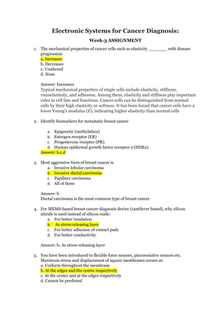
- 1. Electronic Systems for Cancer Diagnosis: Week-3 ASSIGNMENT 1. The mechanical properties of cancer cells such as elasticity _______ with disease progression a. Increases b. Decreases c. Unaltered d. None Answer: Increases Typical mechanical properties of single cells include elasticity, stiffness, viscoelasticity, and adhesion. Among them, elasticity and stiffness play important roles in cell fate and functions. Cancer cells can be distinguished from normal cells by their high elasticity or softness. It has been found that cancer cells have a lower Young's modulus (E), indicating higher elasticity than normal cells 2. Identify biomarkers for metastatic breast cancer a. Epigenetic (methylation) b. Estrogen receptor (ER) c. Progesterone receptor (PR). d. Human epidermal growth factor receptor 2 (HER2) Answer: b,c,d 3. Most aggressive form of breast cancer is a. Invasive lobular carcinoma b. Invasive ductal carcinoma c. Papillary carcinoma d. All of these Answer: b Ductal carcinoma is the most common type of breast cancer 4. For MEMS-based breast cancer diagnosis device (cantilever based), why silicon nitride is used instead of silicon oxide: a. For better insulation b. As stress releasing layer c. For better adhesion of contact pads d. For better conductivity Answer: b. As stress releasing layer 5. You have been introduced to flexible force sensors, piezoresistive sensors etc. Maximum stress and displacement of square membranes occurs at: a. Uniform throughout the membrane b. At the edges and the centre respectively c. At the center and at the edges respectively d. Cannot be predicted
- 2. Answer: At the edges and the centre respectively 6. Why are commercially available silicon wafers circular in shape? a. For fabricating maximum number of devices per unit area b. For ease of handling during process flow execution c. Because the ingot from which it is derived is cylindrical owing to upstream processes d. Making flats to identify the silicon type is easier on circular wafer Answer: Because the ingot from which it is derived is cylindrical owing to upstream processes 7. Lithography process is used to pattern: a. Metal and semiconductor layers b. Metal and insulating layers c. Semiconductor and insulation layers d. Metal, Semiconductor and insulation layers Answer: Metal, Semiconductor and insulation layers 8. Metal deposition is done and then patterned to get the IDE structures which you have seen in the lectures. But metal deposition is usually carried out after deposition of oxide/nitride layer on silicon wafer surface. Why can't metal deposition be carried out directly over silicon? a. Because direct deposition of metal on silicon gives very poor strength and adhesion for the patterns b. Since silicon is a semiconductor, the conductivity effect from bulk will contribute to the conductivity of the metal pattern layer c. Because of constraints from downstream processes such as photolithography d. None of these Answer: Since silicon is a semiconductor, the conductivity effect from bulk will contribute to the conductivity of the metal pattern layer 9. Which of the following processes can produce silicon wafer with more purity: a. CZ technique b. FZ technique c. Boule generation d. Epitaxial growth 10. Which of the following PVD technique can deposit film with better purity? a. E-beam evaporation b. Sputtering c. Thermal evaporation d. Thermal oxidation 11. What is the role of piezoelectric sensor in the disposable MEMS biochip mainly fabricated to study change in tissue properties? a. Study electrical property of tissue
- 3. b. Study mechanical property of tissue c. Study thermal property of tissue d. Study viscoelasticity of tissue 12. Which of the below statements are correct: i. Dry oxidation is about 5 times faster than wet oxidation ii. Dry oxidation is mainly used for creating thin oxide layers and wet oxidation for thicker ones iii. Dry oxidation is used for making field oxide layers and wet oxidation for gate oxides. iv. Dry oxidation gives better quality oxide layers as compared to wet oxidation. a. i, ii, iii, and iv b. ii and iv c. ii, iii and iv d. i, ii, and iv Answer: ii and iv 13. Purpose of the Softbake of photoresistis to reduce residual solvent concentration is to a. Avoid the contamination of the photo mask with resist as well as mask sticking to the resist b. Enhance polymerization c. Improve the resist adhesion to the substrate d. Rapid fabrication Answer: a&c Shortly before the coating step, resist films still contain a substantial amount of residual solvent which depends on the respective film thickness. The subsequent bake step at 90 – 100 °C is performed in order to dry the resist films which would otherwise stick to the mask. Furthermore, the resist layer is hardened during this step, making it more resistant. Besides an improvement of adhesion features, especially the dark field loss during the development step is reduced. 14. Metals and metal compounds such as Ti, Al, Cu, TiN, and TaN can be deposited by a. thermal evaporation b. e-beam evaporation c. sputtering d. All of the above Answer: d Generally, the techniques used to deposit metals are physical, that is, they do not involve achemical reaction. Processes used to deposit semiconducting and insulating layers often involve chemical reactions. The most common methods of physical vapor deposition (PVD) of metal are thermal evaporation, e-beam evaporation, plasma spray deposition, and sputtering. Metals and metal compounds such as Ti, Al, Cu, TiN, and TaN can be deposited by PVD. 15. What is the chemical used in surface conditioning?
- 4. a. HMDS (Hexamethyldixalizane) b. KOH (potassium hydroxide) c. Piranha (sulfuric acid and hydrogen peroxide) d. PMMA (polymethylmethacrylate) Answer: The first step of the Coat Process is Surface Conditioning. Surface conditioning prepares the wafer to accept the photoresist by providing a clean surface, coated with an intermediate chemical (such as HMDS or Hexamethyldisalizane) that creates a hydrophobic surface which boosts adhesion of the photoresist to the wafer’s surface. HMDS is the most commonly used intermediate chemical.