2. 1999 Apr 27 2
Philips Semiconductors Product specification
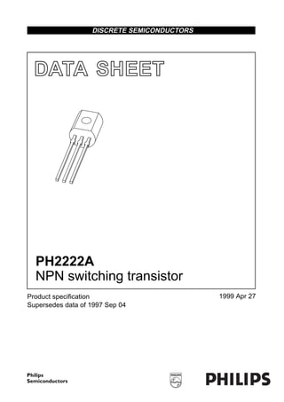
NPN switching transistor PH2222A
FEATURES
• High current (max. 600 mA)
• Low voltage (max. 40 V).
APPLICATIONS
• Switching and linear amplification.
DESCRIPTION
NPN switching transistor in a TO-92; SOT54 plastic
package. PNP complement: PH2907A.
PINNING
PIN DESCRIPTION
1 emitter
2 base
3 collector
Fig.1 Simplified outline (TO-92; SOT54)
and symbol.
handbook, halfpage1
3
2
MAM182
3
2
1
LIMITING VALUES
In accordance with the Absolute Maximum Rating System (IEC 134).
SYMBOL PARAMETER CONDITIONS MIN. MAX. UNIT
VCBO collector-base voltage open emitter − 75 V
VCEO collector-emitter voltage open base − 40 V
VEBO emitter-base voltage open collector − 6 V
IC collector current (DC) − 600 mA
ICM peak collector current − 800 mA
IBM peak base current − 200 mA
Ptot total power dissipation Tamb ≤ 25 °C − 500 mW
Tstg storage temperature −65 +150 °C
Tj junction temperature − 150 °C
Tamb operating ambient temperature −65 +150 °C
3. 1999 Apr 27 3
Philips Semiconductors Product specification
NPN switching transistor PH2222A
THERMAL CHARACTERISTICS
Note
1. Transistor mounted on an FR4 printed-circuit board.
CHARACTERISTICS
Tj = 25 °C unless otherwise specified.
Note
1. Pulse test: tp ≤ 300 µs; δ ≤ 0.02.
SYMBOL PARAMETER CONDITIONS VALUE UNIT
Rth j-a thermal resistance from junction to ambient note 1 250 K/W
SYMBOL PARAMETER CONDITIONS MIN. MAX. UNIT
ICBO collector cut-off current IE = 0; VCB = 60 V − 10 nA
IE = 0; VCB = 60 V; Tamb = 150 °C − 10 µA
IEBO emitter cut-off current IC = 0; VEB = 3 V − 10 nA
hFE DC current gain IC = 0.1 mA; VCE = 10 V 35 −
IC = 1 mA; VCE = 10 V 50 −
IC = 10 mA; VCE = 10 V 75 −
IC = 10 mA; VCE = 10 V; Tamb = −55 °C 35 −
IC = 150 mA; VCE = 1 V; note 1 50 −
IC = 150 mA; VCE = 10 V; note 1 100 300
IC = 500 mA; VCE = 10 V; note 1 40 −
VCEsat collector-emitter saturation voltage IC = 150 mA; IB = 15 mA; note 1 − 300 mV
IC = 500 mA; IB = 50 mA; note 1 − 1 V
VBEsat base-emitter saturation voltage IC = 150 mA; IB = 15 mA; note 1 0.6 1.2 V
IC = 500 mA; IB = 50 mA; note 1 − 2 V
Cc collector capacitance IE = ie = 0; VCB = 10 V; f = 1 MHz − 8 pF
Ce emitter capacitance IC = ic = 0; VEB = 500 mV; f = 1 MHz − 25 pF
fT transition frequency IC = 20 mA; VCE = 20 V; f = 100 MHz 300 − MHz
F noise figure IC = 200 µA; VCE = 5 V; RS = 2 kΩ;
f = 1 kHz; B = 200 Hz
− 4 db
Switching times (between 10% and 90% levels); see Fig.2
ton turn-on time ICon = 150 mA; IBon = 15 mA;
IBoff = −15 mA
− 35 ns
td delay time − 15 ns
tr rise time − 20 ns
toff turn-off time − 250 ns
ts storage time − 200 ns
tf fall time − 60 ns
4. 1999 Apr 27 4
Philips Semiconductors Product specification
NPN switching transistor PH2222A
handbook, full pagewidth
RC
R2
R1
DUT
MLB826
Vo
RB
(probe)
450 Ω
(probe)
450 Ω
oscilloscope oscilloscope
VBB
Vi
VCC
Fig.2 Test circuit for switching times.
Vi = 9.5 V; T = 500 µs; tp = 10 µs; tr = tf ≤ 3 ns.
R1 = 68 Ω; R2 = 325 Ω; RB = 325 Ω; RC = 160 Ω.
VBB = −3.5 V; VCC = 29.5 V.
Oscilloscope: input impedance Zi = 50 Ω.
5. 1999 Apr 27 5
Philips Semiconductors Product specification
NPN switching transistor PH2222A
PACKAGE OUTLINE
UNIT A
REFERENCESOUTLINE
VERSION
EUROPEAN
PROJECTION
ISSUE DATE
IEC JEDEC EIAJ
mm
5.2
5.0
b
0.48
0.40
c
0.45
0.40
D
4.8
4.4
d
1.7
1.4
E
4.2
3.6
L
14.5
12.7
e
2.54
e1
1.27
L1
(1)
2.5
b1
0.66
0.56
DIMENSIONS (mm are the original dimensions)
Note
1. Terminal dimensions within this zone are uncontrolled to allow for flow of plastic and terminal irregularities.
SOT54 TO-92 SC-43 97-02-28
A L
0 2.5 5 mm
scale
b
c
D
b1
L1
d
E
Plastic single-ended leaded (through hole) package; 3 leads SOT54
e1
e
1
2
3
6. 1999 Apr 27 6
Philips Semiconductors Product specification
NPN switching transistor PH2222A
DEFINITIONS
LIFE SUPPORT APPLICATIONS
These products are not designed for use in life support appliances, devices, or systems where malfunction of these
products can reasonably be expected to result in personal injury. Philips customers using or selling these products for
use in such applications do so at their own risk and agree to fully indemnify Philips for any damages resulting from such
improper use or sale.
Data sheet status
Objective specification This data sheet contains target or goal specifications for product development.
Preliminary specification This data sheet contains preliminary data; supplementary data may be published later.
Product specification This data sheet contains final product specifications.
Limiting values
Limiting values given are in accordance with the Absolute Maximum Rating System (IEC 134). Stress above one or
more of the limiting values may cause permanent damage to the device. These are stress ratings only and operation
of the device at these or at any other conditions above those given in the Characteristics sections of the specification
is not implied. Exposure to limiting values for extended periods may affect device reliability.
Application information
Where application information is given, it is advisory and does not form part of the specification.