SlideShare a Scribd company logo
1 of 18
AIM
To design an appropriate logic gate
combination for a given truth table
INTRODUCTION
GATE-A gate is defined as a digital circuit
which follows some logical relationship between
the input and output voltages. It a digital circuit
which allows signal to pass through as stop.
LOGIC GATE- A logic gate is an elementary
building block of a digital circuit. It makes
“logical decisions” based on the different
combinations of digital signals present on its
inputs. Digital logic gates may have more than
one input but generally only have one digital
output. Most logic gates have two inputs and
one output.
A logic gate may have one or more input, but it
has only one output. The relation between the
possible values of input and output voltage is
expressed in the form of table called truth table
or table of combination.
GEORGE BOOLE in 1980 invented a different
kind if algebra based on binary nature at the
logic, this algebra of logic is called BOOLEAN
ALGEBRA. A logical statement can have only
two values, such as HIGH/LOW, ON/OFF,
CLOSED/OPEN, YES/NO, RIGHT/WRONG,
TRUE/FALSE, COUNDUCTING/NON-
COUNDICTING etc. The two values of logic
statement one denoted by the binary number 1
and 0. The binary number 1 is used to denote
high value. The logical statements that logical
gates follow are called Boolean Expression.
LOGIC GATES AND INTEGRATED
CIRCUITS
Logic gates are primarily implemented
electronically using diodes or transistors, but
can also be constructed using electromagnetic
relays logic", fluidic logic, pneumatic
logic, optics, molecules, or even mechanical
elements. With amplification, logic gates can be
cascaded in the same way that Boolean
functions can be composed, allowing the
construction of a physical model of all of
Boolean logic, and therefore, all of the
algorithms and mathematics that can be
described with Boolean logic.
A large number of electronic circuits in
computers, control units, and so on" are made
up of logic gates. These process signals
represent either true or false. $he most
common symbols used to represent logic gates
are shown below.
BASIC GATES
The OR Gate: -
It is a device that combines A and B to give Y as the
result. The OR gate has two or more inputs and one
output. In Boolean algebra, addition symbol (+), is
referred as the OR. The Boolean expression:
A+B=Y
This indicates that Y equals to A or B.
The AND Gate: -
It is a device that combines A with B to give Y as
the result. The AND gate has two or more inputs and
one output. In Boolean algebra, multiplication sign
is referred as the AND. The Boolean expression:
A.B=Y
or
A X B=Y
This indicates that Y equals to A and B.
The NOT Gate: -
It is a device that inverts the inputs. The NOT has
one input and has one output. In Boolean algebra,
bar symbol is referred as the NOT.
The Boolean expression:
A = Y
This indicates that Y is not equal to A.
OR GATE
Aim
TO DESIGN AND SIMULATE THE OR GATE
CIRCUIT.
Components
Two ideal p-n junction diode (D1 and D2).
THEORY AND CONSTRUCTION
An OR gate can be realized by the electronic circuit,
making use of two diodes D1 and D2.
Hear the negative terminal of the batteryis grounded and
correspondsto the 0 level, and the positive terminal of the
battery correspondsto level1. The output Y is voltage at
C with respect to earth.
The following conclusioncan be drawn from the above
circuit:(i)
If the switch A and B are kept open (A=1, B=0), then
bulb does not glow, hence Y=0(ii)
If switch A is kept closed and B is kept open (A=1, B=0),
then bulb does not glow, hence Y=0(iii)
If switch A is kept open and B is kept closed (A=0, B=1),
then bulb does not glow, hence Y=0 (iv)
If switch A and B both are kept closed (A=1, B=1), then
bulb glows, hence Y=1
INPUT A INPUT B OUTPUT Y
0 0 0
1 0 1
0 1 1
AND GATE
AIM
TODESINGANDSTIMULATETHE ANDGATE
CIRCUIT.
Components:
 Two ideal p-n junction diode (D1 and D2)
 A resistance R.
Theory and Construction:
An AND gate can be realized by the electronic circuit,
making use of two diodes D1 and D2. The resistance R is
connectedto the positive terminal of a 5V battery
permanently.
Here the negative terminal of the battery is grounded
and corresponds to the 0 level, and the positive terminal
of the battery corresponds to the level 1. The output Y is
the voltage at C with respect to earth.
The following conclusioncan be easily drawn from the
working of this circuit:
(i) If the switch A and B are kept open (A=0, B=0), then
bulb does not glow., hence Y=0.
(ii) If switch A is kept closed and B is kept open (A=1,
B=0), then bulb does not glow, henceY=0.
(iii) If switch A is kept open and B is kept closed (A=0,
B=1), then bulb does not glow, hence Y=0.
(iv) If both switch A and B are kept closed (A=1, B=1),
then bulb glows, hence Y=1.
INPUT A INPUT B OUTPUT
O 0 0
1 0 0
0 1 0
1 1 1
NOT GATE
Aim:
TO DESIGN AND STIMULATE THE NOT
GATECIRCUIT.
Components:
An ideal n-p-n transistor.
Theory and Construction:
A NOT gate cannot be realized by using diodes.
However, an electroniccircuit of NOT gate can be
realized by making use a n-p-n transistor.
The base of the transistor is connected to the input A
through a resistance Rb and the emitter is earthed. The
collector is connected to 5V battery. The output Y
is voltage at C with respect to earth.
The following inference can be easily drawn from the
working of circuit:
(i) If the switch A is kept open(A=0)then bulb glows,
hence Y=1
(ii) If the switch A is kept closed(A=1) then bulb does not
glow, hence Y=0
INPUT A OUTPUT Y
0 1
1 0
NOR GATE
Aim:
TO DESIGN AND STIMULATE THE NOR GATE
CIRCUIT.
Component:
 Two ideal p-n junction diode (D1 and D2).
 An ideal n-p-n transistor
Theory and Construction:
If we connect the outputY’ of OR gate to the input
of a NOT gate, then the gate obtained is the NOR gate.
The outputY is voltage at C with respect to earth
In Boolean expression, the NOR gate is expressed
as Y=A+B, and is being read as ‘A OR B negated’.
The following interference can be easily drawn from
the working of electrical circuit is
 If Switch A & B open (A=0, B=0) then Lamp will
glow, hence Y=1.
 If Switch A closed & B open (A=1, B=0) then
Lamp will not glow, hence Y=0.
 If Switch A open & B close (A=0, B=1) then
Lamp will not glow, hence Y=0.
 If switch A & B are closed then (A=1, B=1)
Lamp will not glow, hence Y=0.
INPUT A INPUT B OUTPUT Y
0 0 1
1 0 0
0 1 0
1 1 0
THE NAND GATE
Aim:
TO DESIGN AND SIMULATE THE NAND GATE
CIRCUIT.
Components:
Two ideal p-n junction diode (D1 and D2),a resistance R,
an ideal n-p- n transistor.
Theory and construction:
If we connect the output Y’ of AND gate to the input
of a NOT gate the gate obtained is called NAND
gate.
The output Y is voltage at C w.r.t. earth.
In Boolean expression the NAND gate is
expressed as Y=A.B, and is being read as ‘A AND
B negated’. The following interference can be
easily drawn from the working of electrical circuit:
 If Switch A & B open (A=0, B=0) then Lamp will
glow, hence Y=1.
 If Switch A open B closed then (A=0, B=1) Lamp
glow, hence Y=1.
 If switch A closed B open then (A=1, B=0) Lamp
glow, hence Y=1.
 If switch A & B are closed then (A=1, B=1) Lamp
will not glow, hence Y=0.
INPUT A INPUT B OUTPUT Y
0 0 1
1 0 1
0 1 1
1 1 0
BIBLIOGRAPHY
I obtained my information on this topic through-
 Slideshare.com
 Wikipedia.org
 Physics manual

More Related Content

What's hot

Physics project on logic gate
Physics project on logic gatePhysics project on logic gate
Physics project on logic gateVirat Prasad
 
296779866 c-b-s-e-class-12-physics-project-on-logic-gates
296779866 c-b-s-e-class-12-physics-project-on-logic-gates296779866 c-b-s-e-class-12-physics-project-on-logic-gates
296779866 c-b-s-e-class-12-physics-project-on-logic-gatesAnuragSharma530
 
Class 12 Physics Investigatory Project Work, Practical- study of various logi...
Class 12 Physics Investigatory Project Work, Practical- study of various logi...Class 12 Physics Investigatory Project Work, Practical- study of various logi...
Class 12 Physics Investigatory Project Work, Practical- study of various logi...Kendriya Vidyalaya
 
Report on-the-logic-gates
Report on-the-logic-gatesReport on-the-logic-gates
Report on-the-logic-gatesbhardubhai
 
logic gates using IC cbse class 12
logic gates using IC cbse class 12logic gates using IC cbse class 12
logic gates using IC cbse class 12Kirthi Kirthu
 
Logic Gates Class 12
Logic Gates Class 12Logic Gates Class 12
Logic Gates Class 12RithuJ
 
Physics logic gates1
Physics logic gates1Physics logic gates1
Physics logic gates1Kirthi Kirthu
 
Physics investigatory project
Physics investigatory projectPhysics investigatory project
Physics investigatory projectPrakhar Seth
 
Chemistry investigatory project
Chemistry investigatory projectChemistry investigatory project
Chemistry investigatory projectAbhinav Kumar
 
Physics investigatory project for class 12 logic gates
Physics investigatory project for class 12 logic gatesPhysics investigatory project for class 12 logic gates
Physics investigatory project for class 12 logic gatesbiswanath dehuri
 
Chemistry investigatory project
Chemistry investigatory projectChemistry investigatory project
Chemistry investigatory projectSushmithaR26
 
Chemistryprojectoncaseininmik 170207030628
Chemistryprojectoncaseininmik 170207030628Chemistryprojectoncaseininmik 170207030628
Chemistryprojectoncaseininmik 170207030628AnuragSharma530
 
Microbes in human welfare
Microbes in human welfareMicrobes in human welfare
Microbes in human welfareRajveer Atal
 
Physics investigatory project
Physics investigatory projectPhysics investigatory project
Physics investigatory projectNIKHIL DWIVEDI
 
PHYSICS INVESTIGATORY PROJECT 2017-18
PHYSICS INVESTIGATORY PROJECT 2017-18PHYSICS INVESTIGATORY PROJECT 2017-18
PHYSICS INVESTIGATORY PROJECT 2017-18HIMANSHU .
 
Various factors on which the internal resistance of a cell depends
Various factors on which the internal resistance of a cell dependsVarious factors on which the internal resistance of a cell depends
Various factors on which the internal resistance of a cell dependsParthMehray
 

What's hot (20)

Physics project on logic gate
Physics project on logic gatePhysics project on logic gate
Physics project on logic gate
 
296779866 c-b-s-e-class-12-physics-project-on-logic-gates
296779866 c-b-s-e-class-12-physics-project-on-logic-gates296779866 c-b-s-e-class-12-physics-project-on-logic-gates
296779866 c-b-s-e-class-12-physics-project-on-logic-gates
 
Physic investigatory
Physic investigatoryPhysic investigatory
Physic investigatory
 
Class 12 Physics Investigatory Project Work, Practical- study of various logi...
Class 12 Physics Investigatory Project Work, Practical- study of various logi...Class 12 Physics Investigatory Project Work, Practical- study of various logi...
Class 12 Physics Investigatory Project Work, Practical- study of various logi...
 
Report on-the-logic-gates
Report on-the-logic-gatesReport on-the-logic-gates
Report on-the-logic-gates
 
logic gates using IC cbse class 12
logic gates using IC cbse class 12logic gates using IC cbse class 12
logic gates using IC cbse class 12
 
Logic Gates Class 12
Logic Gates Class 12Logic Gates Class 12
Logic Gates Class 12
 
Physics logic gates1
Physics logic gates1Physics logic gates1
Physics logic gates1
 
Physics investigatory project
Physics investigatory projectPhysics investigatory project
Physics investigatory project
 
Chemistry investigatory project
Chemistry investigatory projectChemistry investigatory project
Chemistry investigatory project
 
Physics investigatory project for class 12 logic gates
Physics investigatory project for class 12 logic gatesPhysics investigatory project for class 12 logic gates
Physics investigatory project for class 12 logic gates
 
Chemistry investigatory project
Chemistry investigatory projectChemistry investigatory project
Chemistry investigatory project
 
Chemistryprojectoncaseininmik 170207030628
Chemistryprojectoncaseininmik 170207030628Chemistryprojectoncaseininmik 170207030628
Chemistryprojectoncaseininmik 170207030628
 
Wheatstone Bridge
Wheatstone BridgeWheatstone Bridge
Wheatstone Bridge
 
Microbes in human welfare
Microbes in human welfareMicrobes in human welfare
Microbes in human welfare
 
Physics investigatory project
Physics investigatory projectPhysics investigatory project
Physics investigatory project
 
PHYSICS INVESTIGATORY PROJECT 2017-18
PHYSICS INVESTIGATORY PROJECT 2017-18PHYSICS INVESTIGATORY PROJECT 2017-18
PHYSICS INVESTIGATORY PROJECT 2017-18
 
Chemistry
ChemistryChemistry
Chemistry
 
Physics investigatory project
Physics investigatory projectPhysics investigatory project
Physics investigatory project
 
Various factors on which the internal resistance of a cell depends
Various factors on which the internal resistance of a cell dependsVarious factors on which the internal resistance of a cell depends
Various factors on which the internal resistance of a cell depends
 

Similar to physics investigatory on logic gates

Physics_Investigatory_Project_on_Logic_G.pptx
Physics_Investigatory_Project_on_Logic_G.pptxPhysics_Investigatory_Project_on_Logic_G.pptx
Physics_Investigatory_Project_on_Logic_G.pptxNitinMaurya62
 
PHYSICS PROJECT 12.pptx
PHYSICS PROJECT 12.pptxPHYSICS PROJECT 12.pptx
PHYSICS PROJECT 12.pptxDronBansal
 
Physics logic gates 2
Physics logic gates 2Physics logic gates 2
Physics logic gates 2Kirthi Kirthu
 
LOGIC GATE ||CLASS 12 PHYSICS I
LOGIC GATE ||CLASS 12 PHYSICS ILOGIC GATE ||CLASS 12 PHYSICS I
LOGIC GATE ||CLASS 12 PHYSICS IAryan137
 
solids_and_semiconductor_devices_4.ppt
solids_and_semiconductor_devices_4.pptsolids_and_semiconductor_devices_4.ppt
solids_and_semiconductor_devices_4.pptUmeshPatil149
 
Solids_And_Semiconductor_Devices_4.ppt
Solids_And_Semiconductor_Devices_4.pptSolids_And_Semiconductor_Devices_4.ppt
Solids_And_Semiconductor_Devices_4.pptJosephMuez2
 
Semiconductor Devices Class 12 Part-4
Semiconductor Devices Class 12 Part-4Semiconductor Devices Class 12 Part-4
Semiconductor Devices Class 12 Part-4Self-employed
 
1,basic and derived logic gates.pdf
1,basic and derived logic gates.pdf1,basic and derived logic gates.pdf
1,basic and derived logic gates.pdfDamotTesfaye
 
PHYSICS PRACTICAL PROJECT (1).pdf
PHYSICS PRACTICAL PROJECT (1).pdfPHYSICS PRACTICAL PROJECT (1).pdf
PHYSICS PRACTICAL PROJECT (1).pdfOmChaubey7
 
boolean algrebra and logic gates in short
boolean algrebra and logic gates in shortboolean algrebra and logic gates in short
boolean algrebra and logic gates in shortRojin Khadka
 
Digital logic gates and Boolean algebra
Digital logic gates and Boolean algebraDigital logic gates and Boolean algebra
Digital logic gates and Boolean algebraSARITHA REDDY
 
Lecture 04-Digital logic gates.pptx
Lecture 04-Digital logic gates.pptxLecture 04-Digital logic gates.pptx
Lecture 04-Digital logic gates.pptxWilliamJosephat1
 
Chapter 4. logic function and boolean algebra
Chapter 4. logic function and boolean algebraChapter 4. logic function and boolean algebra
Chapter 4. logic function and boolean algebraAshish KC
 

Similar to physics investigatory on logic gates (20)

Physics_Investigatory_Project_on_Logic_G.pptx
Physics_Investigatory_Project_on_Logic_G.pptxPhysics_Investigatory_Project_on_Logic_G.pptx
Physics_Investigatory_Project_on_Logic_G.pptx
 
PHYSICS PROJECT 12.pptx
PHYSICS PROJECT 12.pptxPHYSICS PROJECT 12.pptx
PHYSICS PROJECT 12.pptx
 
Physics logic gates 2
Physics logic gates 2Physics logic gates 2
Physics logic gates 2
 
Digital logic
Digital logicDigital logic
Digital logic
 
Class 12th Logic Gates
Class 12th Logic GatesClass 12th Logic Gates
Class 12th Logic Gates
 
LOGIC GATE ||CLASS 12 PHYSICS I
LOGIC GATE ||CLASS 12 PHYSICS ILOGIC GATE ||CLASS 12 PHYSICS I
LOGIC GATE ||CLASS 12 PHYSICS I
 
solids_and_semiconductor_devices_4.ppt
solids_and_semiconductor_devices_4.pptsolids_and_semiconductor_devices_4.ppt
solids_and_semiconductor_devices_4.ppt
 
Solids_And_Semiconductor_Devices_4.ppt
Solids_And_Semiconductor_Devices_4.pptSolids_And_Semiconductor_Devices_4.ppt
Solids_And_Semiconductor_Devices_4.ppt
 
Semiconductor Devices Class 12 Part-4
Semiconductor Devices Class 12 Part-4Semiconductor Devices Class 12 Part-4
Semiconductor Devices Class 12 Part-4
 
1,basic and derived logic gates.pdf
1,basic and derived logic gates.pdf1,basic and derived logic gates.pdf
1,basic and derived logic gates.pdf
 
Logic gates
Logic gatesLogic gates
Logic gates
 
PHYSICS PRACTICAL PROJECT (1).pdf
PHYSICS PRACTICAL PROJECT (1).pdfPHYSICS PRACTICAL PROJECT (1).pdf
PHYSICS PRACTICAL PROJECT (1).pdf
 
boolean algrebra and logic gates in short
boolean algrebra and logic gates in shortboolean algrebra and logic gates in short
boolean algrebra and logic gates in short
 
Digital logic gates and Boolean algebra
Digital logic gates and Boolean algebraDigital logic gates and Boolean algebra
Digital logic gates and Boolean algebra
 
logic gates
logic gateslogic gates
logic gates
 
Logic gates (1)
Logic gates (1)Logic gates (1)
Logic gates (1)
 
SEMICONDUCTORS
SEMICONDUCTORSSEMICONDUCTORS
SEMICONDUCTORS
 
Lecture 04-Digital logic gates.pptx
Lecture 04-Digital logic gates.pptxLecture 04-Digital logic gates.pptx
Lecture 04-Digital logic gates.pptx
 
Deld lab manual
Deld lab manualDeld lab manual
Deld lab manual
 
Chapter 4. logic function and boolean algebra
Chapter 4. logic function and boolean algebraChapter 4. logic function and boolean algebra
Chapter 4. logic function and boolean algebra
 

Recently uploaded

How to Configure Email Server in Odoo 17
How to Configure Email Server in Odoo 17How to Configure Email Server in Odoo 17
How to Configure Email Server in Odoo 17Celine George
 
Historical philosophical, theoretical, and legal foundations of special and i...
Historical philosophical, theoretical, and legal foundations of special and i...Historical philosophical, theoretical, and legal foundations of special and i...
Historical philosophical, theoretical, and legal foundations of special and i...jaredbarbolino94
 
Pharmacognosy Flower 3. Compositae 2023.pdf
Pharmacognosy Flower 3. Compositae 2023.pdfPharmacognosy Flower 3. Compositae 2023.pdf
Pharmacognosy Flower 3. Compositae 2023.pdfMahmoud M. Sallam
 
Alper Gobel In Media Res Media Component
Alper Gobel In Media Res Media ComponentAlper Gobel In Media Res Media Component
Alper Gobel In Media Res Media ComponentInMediaRes1
 
MARGINALIZATION (Different learners in Marginalized Group
MARGINALIZATION (Different learners in Marginalized GroupMARGINALIZATION (Different learners in Marginalized Group
MARGINALIZATION (Different learners in Marginalized GroupJonathanParaisoCruz
 
EPANDING THE CONTENT OF AN OUTLINE using notes.pptx
EPANDING THE CONTENT OF AN OUTLINE using notes.pptxEPANDING THE CONTENT OF AN OUTLINE using notes.pptx
EPANDING THE CONTENT OF AN OUTLINE using notes.pptxRaymartEstabillo3
 
Framing an Appropriate Research Question 6b9b26d93da94caf993c038d9efcdedb.pdf
Framing an Appropriate Research Question 6b9b26d93da94caf993c038d9efcdedb.pdfFraming an Appropriate Research Question 6b9b26d93da94caf993c038d9efcdedb.pdf
Framing an Appropriate Research Question 6b9b26d93da94caf993c038d9efcdedb.pdfUjwalaBharambe
 
CELL CYCLE Division Science 8 quarter IV.pptx
CELL CYCLE Division Science 8 quarter IV.pptxCELL CYCLE Division Science 8 quarter IV.pptx
CELL CYCLE Division Science 8 quarter IV.pptxJiesonDelaCerna
 
Proudly South Africa powerpoint Thorisha.pptx
Proudly South Africa powerpoint Thorisha.pptxProudly South Africa powerpoint Thorisha.pptx
Proudly South Africa powerpoint Thorisha.pptxthorishapillay1
 
internship ppt on smartinternz platform as salesforce developer
internship ppt on smartinternz platform as salesforce developerinternship ppt on smartinternz platform as salesforce developer
internship ppt on smartinternz platform as salesforce developerunnathinaik
 
Final demo Grade 9 for demo Plan dessert.pptx
Final demo Grade 9 for demo Plan dessert.pptxFinal demo Grade 9 for demo Plan dessert.pptx
Final demo Grade 9 for demo Plan dessert.pptxAvyJaneVismanos
 
ECONOMIC CONTEXT - LONG FORM TV DRAMA - PPT
ECONOMIC CONTEXT - LONG FORM TV DRAMA - PPTECONOMIC CONTEXT - LONG FORM TV DRAMA - PPT
ECONOMIC CONTEXT - LONG FORM TV DRAMA - PPTiammrhaywood
 
Organic Name Reactions for the students and aspirants of Chemistry12th.pptx
Organic Name Reactions  for the students and aspirants of Chemistry12th.pptxOrganic Name Reactions  for the students and aspirants of Chemistry12th.pptx
Organic Name Reactions for the students and aspirants of Chemistry12th.pptxVS Mahajan Coaching Centre
 
भारत-रोम व्यापार.pptx, Indo-Roman Trade,
भारत-रोम व्यापार.pptx, Indo-Roman Trade,भारत-रोम व्यापार.pptx, Indo-Roman Trade,
भारत-रोम व्यापार.pptx, Indo-Roman Trade,Virag Sontakke
 
Solving Puzzles Benefits Everyone (English).pptx
Solving Puzzles Benefits Everyone (English).pptxSolving Puzzles Benefits Everyone (English).pptx
Solving Puzzles Benefits Everyone (English).pptxOH TEIK BIN
 
KSHARA STURA .pptx---KSHARA KARMA THERAPY (CAUSTIC THERAPY)————IMP.OF KSHARA ...
KSHARA STURA .pptx---KSHARA KARMA THERAPY (CAUSTIC THERAPY)————IMP.OF KSHARA ...KSHARA STURA .pptx---KSHARA KARMA THERAPY (CAUSTIC THERAPY)————IMP.OF KSHARA ...
KSHARA STURA .pptx---KSHARA KARMA THERAPY (CAUSTIC THERAPY)————IMP.OF KSHARA ...M56BOOKSTORE PRODUCT/SERVICE
 
“Oh GOSH! Reflecting on Hackteria's Collaborative Practices in a Global Do-It...
“Oh GOSH! Reflecting on Hackteria's Collaborative Practices in a Global Do-It...“Oh GOSH! Reflecting on Hackteria's Collaborative Practices in a Global Do-It...
“Oh GOSH! Reflecting on Hackteria's Collaborative Practices in a Global Do-It...Marc Dusseiller Dusjagr
 

Recently uploaded (20)

How to Configure Email Server in Odoo 17
How to Configure Email Server in Odoo 17How to Configure Email Server in Odoo 17
How to Configure Email Server in Odoo 17
 
9953330565 Low Rate Call Girls In Rohini Delhi NCR
9953330565 Low Rate Call Girls In Rohini  Delhi NCR9953330565 Low Rate Call Girls In Rohini  Delhi NCR
9953330565 Low Rate Call Girls In Rohini Delhi NCR
 
Historical philosophical, theoretical, and legal foundations of special and i...
Historical philosophical, theoretical, and legal foundations of special and i...Historical philosophical, theoretical, and legal foundations of special and i...
Historical philosophical, theoretical, and legal foundations of special and i...
 
Pharmacognosy Flower 3. Compositae 2023.pdf
Pharmacognosy Flower 3. Compositae 2023.pdfPharmacognosy Flower 3. Compositae 2023.pdf
Pharmacognosy Flower 3. Compositae 2023.pdf
 
Alper Gobel In Media Res Media Component
Alper Gobel In Media Res Media ComponentAlper Gobel In Media Res Media Component
Alper Gobel In Media Res Media Component
 
MARGINALIZATION (Different learners in Marginalized Group
MARGINALIZATION (Different learners in Marginalized GroupMARGINALIZATION (Different learners in Marginalized Group
MARGINALIZATION (Different learners in Marginalized Group
 
EPANDING THE CONTENT OF AN OUTLINE using notes.pptx
EPANDING THE CONTENT OF AN OUTLINE using notes.pptxEPANDING THE CONTENT OF AN OUTLINE using notes.pptx
EPANDING THE CONTENT OF AN OUTLINE using notes.pptx
 
Framing an Appropriate Research Question 6b9b26d93da94caf993c038d9efcdedb.pdf
Framing an Appropriate Research Question 6b9b26d93da94caf993c038d9efcdedb.pdfFraming an Appropriate Research Question 6b9b26d93da94caf993c038d9efcdedb.pdf
Framing an Appropriate Research Question 6b9b26d93da94caf993c038d9efcdedb.pdf
 
CELL CYCLE Division Science 8 quarter IV.pptx
CELL CYCLE Division Science 8 quarter IV.pptxCELL CYCLE Division Science 8 quarter IV.pptx
CELL CYCLE Division Science 8 quarter IV.pptx
 
Proudly South Africa powerpoint Thorisha.pptx
Proudly South Africa powerpoint Thorisha.pptxProudly South Africa powerpoint Thorisha.pptx
Proudly South Africa powerpoint Thorisha.pptx
 
internship ppt on smartinternz platform as salesforce developer
internship ppt on smartinternz platform as salesforce developerinternship ppt on smartinternz platform as salesforce developer
internship ppt on smartinternz platform as salesforce developer
 
Final demo Grade 9 for demo Plan dessert.pptx
Final demo Grade 9 for demo Plan dessert.pptxFinal demo Grade 9 for demo Plan dessert.pptx
Final demo Grade 9 for demo Plan dessert.pptx
 
TataKelola dan KamSiber Kecerdasan Buatan v022.pdf
TataKelola dan KamSiber Kecerdasan Buatan v022.pdfTataKelola dan KamSiber Kecerdasan Buatan v022.pdf
TataKelola dan KamSiber Kecerdasan Buatan v022.pdf
 
ECONOMIC CONTEXT - LONG FORM TV DRAMA - PPT
ECONOMIC CONTEXT - LONG FORM TV DRAMA - PPTECONOMIC CONTEXT - LONG FORM TV DRAMA - PPT
ECONOMIC CONTEXT - LONG FORM TV DRAMA - PPT
 
OS-operating systems- ch04 (Threads) ...
OS-operating systems- ch04 (Threads) ...OS-operating systems- ch04 (Threads) ...
OS-operating systems- ch04 (Threads) ...
 
Organic Name Reactions for the students and aspirants of Chemistry12th.pptx
Organic Name Reactions  for the students and aspirants of Chemistry12th.pptxOrganic Name Reactions  for the students and aspirants of Chemistry12th.pptx
Organic Name Reactions for the students and aspirants of Chemistry12th.pptx
 
भारत-रोम व्यापार.pptx, Indo-Roman Trade,
भारत-रोम व्यापार.pptx, Indo-Roman Trade,भारत-रोम व्यापार.pptx, Indo-Roman Trade,
भारत-रोम व्यापार.pptx, Indo-Roman Trade,
 
Solving Puzzles Benefits Everyone (English).pptx
Solving Puzzles Benefits Everyone (English).pptxSolving Puzzles Benefits Everyone (English).pptx
Solving Puzzles Benefits Everyone (English).pptx
 
KSHARA STURA .pptx---KSHARA KARMA THERAPY (CAUSTIC THERAPY)————IMP.OF KSHARA ...
KSHARA STURA .pptx---KSHARA KARMA THERAPY (CAUSTIC THERAPY)————IMP.OF KSHARA ...KSHARA STURA .pptx---KSHARA KARMA THERAPY (CAUSTIC THERAPY)————IMP.OF KSHARA ...
KSHARA STURA .pptx---KSHARA KARMA THERAPY (CAUSTIC THERAPY)————IMP.OF KSHARA ...
 
“Oh GOSH! Reflecting on Hackteria's Collaborative Practices in a Global Do-It...
“Oh GOSH! Reflecting on Hackteria's Collaborative Practices in a Global Do-It...“Oh GOSH! Reflecting on Hackteria's Collaborative Practices in a Global Do-It...
“Oh GOSH! Reflecting on Hackteria's Collaborative Practices in a Global Do-It...
 

physics investigatory on logic gates

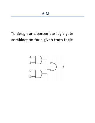
  • 1. AIM To design an appropriate logic gate combination for a given truth table
  • 2. INTRODUCTION GATE-A gate is defined as a digital circuit which follows some logical relationship between the input and output voltages. It a digital circuit which allows signal to pass through as stop. LOGIC GATE- A logic gate is an elementary building block of a digital circuit. It makes “logical decisions” based on the different combinations of digital signals present on its inputs. Digital logic gates may have more than one input but generally only have one digital output. Most logic gates have two inputs and one output. A logic gate may have one or more input, but it has only one output. The relation between the possible values of input and output voltage is expressed in the form of table called truth table or table of combination.
  • 3. GEORGE BOOLE in 1980 invented a different kind if algebra based on binary nature at the logic, this algebra of logic is called BOOLEAN ALGEBRA. A logical statement can have only two values, such as HIGH/LOW, ON/OFF, CLOSED/OPEN, YES/NO, RIGHT/WRONG, TRUE/FALSE, COUNDUCTING/NON- COUNDICTING etc. The two values of logic statement one denoted by the binary number 1 and 0. The binary number 1 is used to denote high value. The logical statements that logical gates follow are called Boolean Expression.
  • 4. LOGIC GATES AND INTEGRATED CIRCUITS Logic gates are primarily implemented electronically using diodes or transistors, but can also be constructed using electromagnetic relays logic", fluidic logic, pneumatic logic, optics, molecules, or even mechanical elements. With amplification, logic gates can be cascaded in the same way that Boolean functions can be composed, allowing the construction of a physical model of all of Boolean logic, and therefore, all of the algorithms and mathematics that can be described with Boolean logic. A large number of electronic circuits in computers, control units, and so on" are made up of logic gates. These process signals represent either true or false. $he most common symbols used to represent logic gates are shown below.
  • 5. BASIC GATES The OR Gate: - It is a device that combines A and B to give Y as the result. The OR gate has two or more inputs and one output. In Boolean algebra, addition symbol (+), is referred as the OR. The Boolean expression: A+B=Y This indicates that Y equals to A or B. The AND Gate: - It is a device that combines A with B to give Y as the result. The AND gate has two or more inputs and one output. In Boolean algebra, multiplication sign is referred as the AND. The Boolean expression: A.B=Y or A X B=Y This indicates that Y equals to A and B.
  • 6. The NOT Gate: - It is a device that inverts the inputs. The NOT has one input and has one output. In Boolean algebra, bar symbol is referred as the NOT. The Boolean expression: A = Y This indicates that Y is not equal to A.
  • 7. OR GATE Aim TO DESIGN AND SIMULATE THE OR GATE CIRCUIT. Components Two ideal p-n junction diode (D1 and D2). THEORY AND CONSTRUCTION An OR gate can be realized by the electronic circuit, making use of two diodes D1 and D2. Hear the negative terminal of the batteryis grounded and correspondsto the 0 level, and the positive terminal of the battery correspondsto level1. The output Y is voltage at C with respect to earth.
  • 8. The following conclusioncan be drawn from the above circuit:(i) If the switch A and B are kept open (A=1, B=0), then bulb does not glow, hence Y=0(ii) If switch A is kept closed and B is kept open (A=1, B=0), then bulb does not glow, hence Y=0(iii) If switch A is kept open and B is kept closed (A=0, B=1), then bulb does not glow, hence Y=0 (iv) If switch A and B both are kept closed (A=1, B=1), then bulb glows, hence Y=1 INPUT A INPUT B OUTPUT Y 0 0 0 1 0 1 0 1 1
  • 9. AND GATE AIM TODESINGANDSTIMULATETHE ANDGATE CIRCUIT. Components:  Two ideal p-n junction diode (D1 and D2)  A resistance R. Theory and Construction: An AND gate can be realized by the electronic circuit, making use of two diodes D1 and D2. The resistance R is connectedto the positive terminal of a 5V battery permanently. Here the negative terminal of the battery is grounded and corresponds to the 0 level, and the positive terminal of the battery corresponds to the level 1. The output Y is the voltage at C with respect to earth.
  • 10. The following conclusioncan be easily drawn from the working of this circuit: (i) If the switch A and B are kept open (A=0, B=0), then bulb does not glow., hence Y=0. (ii) If switch A is kept closed and B is kept open (A=1, B=0), then bulb does not glow, henceY=0. (iii) If switch A is kept open and B is kept closed (A=0, B=1), then bulb does not glow, hence Y=0. (iv) If both switch A and B are kept closed (A=1, B=1), then bulb glows, hence Y=1. INPUT A INPUT B OUTPUT O 0 0 1 0 0
  • 11. 0 1 0 1 1 1
  • 12. NOT GATE Aim: TO DESIGN AND STIMULATE THE NOT GATECIRCUIT. Components: An ideal n-p-n transistor. Theory and Construction: A NOT gate cannot be realized by using diodes. However, an electroniccircuit of NOT gate can be realized by making use a n-p-n transistor. The base of the transistor is connected to the input A through a resistance Rb and the emitter is earthed. The collector is connected to 5V battery. The output Y is voltage at C with respect to earth.
  • 13. The following inference can be easily drawn from the working of circuit: (i) If the switch A is kept open(A=0)then bulb glows, hence Y=1 (ii) If the switch A is kept closed(A=1) then bulb does not glow, hence Y=0 INPUT A OUTPUT Y 0 1 1 0
  • 14. NOR GATE Aim: TO DESIGN AND STIMULATE THE NOR GATE CIRCUIT. Component:  Two ideal p-n junction diode (D1 and D2).  An ideal n-p-n transistor Theory and Construction: If we connect the outputY’ of OR gate to the input of a NOT gate, then the gate obtained is the NOR gate. The outputY is voltage at C with respect to earth In Boolean expression, the NOR gate is expressed as Y=A+B, and is being read as ‘A OR B negated’. The following interference can be easily drawn from the working of electrical circuit is  If Switch A & B open (A=0, B=0) then Lamp will glow, hence Y=1.
  • 15.  If Switch A closed & B open (A=1, B=0) then Lamp will not glow, hence Y=0.  If Switch A open & B close (A=0, B=1) then Lamp will not glow, hence Y=0.  If switch A & B are closed then (A=1, B=1) Lamp will not glow, hence Y=0. INPUT A INPUT B OUTPUT Y 0 0 1 1 0 0 0 1 0 1 1 0
  • 16. THE NAND GATE Aim: TO DESIGN AND SIMULATE THE NAND GATE CIRCUIT. Components: Two ideal p-n junction diode (D1 and D2),a resistance R, an ideal n-p- n transistor. Theory and construction: If we connect the output Y’ of AND gate to the input of a NOT gate the gate obtained is called NAND gate. The output Y is voltage at C w.r.t. earth.
  • 17. In Boolean expression the NAND gate is expressed as Y=A.B, and is being read as ‘A AND B negated’. The following interference can be easily drawn from the working of electrical circuit:  If Switch A & B open (A=0, B=0) then Lamp will glow, hence Y=1.  If Switch A open B closed then (A=0, B=1) Lamp glow, hence Y=1.  If switch A closed B open then (A=1, B=0) Lamp glow, hence Y=1.  If switch A & B are closed then (A=1, B=1) Lamp will not glow, hence Y=0. INPUT A INPUT B OUTPUT Y 0 0 1 1 0 1 0 1 1 1 1 0
  • 18. BIBLIOGRAPHY I obtained my information on this topic through-  Slideshare.com  Wikipedia.org  Physics manual