The iot academy_embeddedsystems_training_circuitdesignpart3
Sequential Circuit Optimization
1. Sequential Circuit Optimization
By: Mary Dillon
Introduction:
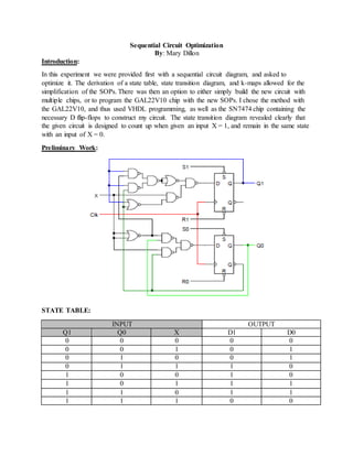
In this experiment we were provided first with a sequential circuit diagram, and asked to
optimize it. The derivation of a state table, state transition diagram, and k-maps allowed for the
simplification of the SOPs. There was then an option to either simply build the new circuit with
multiple chips, or to program the GAL22V10 chip with the new SOPs. I chose the method with
the GAL22V10, and thus used VHDL programming, as well as the SN7474 chip containing the
necessary D flip-flops to construct my circuit. The state transition diagram revealed clearly that
the given circuit is designed to count up when given an input X = 1, and remain in the same state
with an input of X = 0.
Preliminary Work:
STATE TABLE:
INPUT OUTPUT
Q1 Q0 X D1 D0
0 0 0 0 0
0 0 1 0 1
0 1 0 0 1
0 1 1 1 0
1 0 0 1 0
1 0 1 1 1
1 1 0 1 1
1 1 1 0 0
3. VHDL CODE:
library IEEE;
use IEEE.STD_LOGIC_1164.all;
entity deathstar is PORT(
X : in std_logic;
Q_0 : in std_logic;
Q_1: in std_logic;
D1: out std_logic;
D2 : out std_logic);
end deathstar;
architecture deathstar of deathstar is begin
-- enter your EQUATIONS here
D1 <= ((not Q_1) and Q_0 and X) OR (Q_1 and (not X)) OR (Q_1 and (not Q_0));
D2 <= ((not Q_0) and X) OR (Q_0 and (not X));
end deathstar;
Stimulus for testbench:
C <= '0', '1' after 20ns, '0' after 40ns, '1' after 60ns, '0' after 80ns, '1'
after 100ns, '0' after 120ns, '1' after 140ns, '0' after 160ns;
B <= '0', '1' after 40ns, '0' after 80ns, '1' after 120ns, '0' after 160ns;
A <= '0', '1' after 80ns, '0' after 160ns;
CHIP DIAGRAMS:
4. WIRE LIST:
U1 = GAL22V10
U2 = SN7474
U1 – 12 GND
U1 – 24 VCC
U2 – 7 GND
U2 – 14 VCC
U1 – 1 SW1 R1 GND
U1 – 2 U2 – 9
U1 – 3 U2 – 5
U1 – 23 U2 – 2
U1 – 14 U2 – 12
U2 – 2 LED1 R2 GND
U2 – 12 LED2 R3 GND
Lab Results:
The circuit worked properly. The test LEDs lit up to represent the correct states defined in the
state table derived from the original circuit configuration.
Observations and Conclusions:
At first, the LEDs were not lighting up to represent the correct states, and after checking the state
table, diagram, and SOPs it was determined that it was a hardware issue. As a whole, the
GAL22V10 chip made this circuit far easier to construct. Instead of using four or five chips with
different gates, I only needed to use two chips. This, and the significantly smaller amount of
wires required for the circuit allows for a smaller probability for error and troubleshooting.
Circuit Modifications:
The hardware issue was found to be within the SN7474 chip, which seemed to only have one
functioning flip-flop. I replaced it with a new SN7474, and the correct states were achieved. I
also originally started working on the circuit with the four or five chip approach, but once I
became familiar with the GAL chip, I determined that using it would be far simpler and more
efficient.