1. 11 ML
4 ML
6 ML
Southampton
Unive rsity
Micro e le ctro nics
Ce ntre
Structural and Compositional Evolution of Self-Assembled
Germanium Islands on Silicon (001) During High Growth Rate LPCVD
Gabriela D.M. Dilliway1
, Nicholas E.B. Cowern2
, Chris Jeynes2
, Lisa O’Reilly3
, Patrick J. McNally3
, Darren M. Bagnall1
1
Dept. of Electronics and Computer Science, Univ. of Southampton, Highfield, Southampton SO17 1BJ, UK, G.D.M.Dilliway@soton.ac.uk
2
Advanced Technology Institute, Univ. of Surrey, Guildford GU2 7XH, UK
3
Research Institute for Networks & Communications Engineering (RINCE), School of Electronic Engineering, Dublin City University, Dublin 9, Ireland
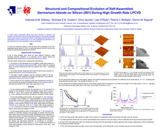
0 20 40 60 0 100 200 300
Height (nm) Width (nm)
0 20 40 60 0 100 200 300
Height (nm) Width (nm)
Islandfrequency(arbitraryunits)
(a)
(b)
(c)
In recent years, substantial efforts have been devoted to research into
quantum dot structures due to the interesting electronic and optical properties
resulting from quantum confinement effects. Understanding the process of self-
organization of Ge nanostructures on Si with controlled size distribution is a
key requirement for their application to device fabrication.
Aim
To study the temporal evolution of the structure and composition of Ge self-
assembled islands grown on (001) Si using high growth rate (6-9 nm/min) low
pressure chemical vapour deposition (LPCVD).
Experimental Techniques
A set of three samples were grown for three different durations, under
nominally identical conditions, in a cold-wall LPCVD reactor design and
fabricated at the Southampton University Microelectronics Centre.
The three grown samples were subsequently characterised:
The amount of Ge deposited and its crystalline quality were studied by
Rutherford backscattering spectroscopy (RBS), using a 2 MeV He analysing
beam at normal incidence and both the ‘random’ and <100> channelling
directions.
The surface density, shape and size of the Ge islands were analysed by
contact mode atomic force microscopy (AFM).
The state of strain relaxation and the crystalline quality of the Ge
nanostructures were assessed with bright and dark-field cross-sectional
transmission electron microscopy (XTEM).
Further insight into the crystalline quality and compositional evolution of
the Ge islands was obtained by detailed analysis of micro-Raman spectra,
obtained using a 488 nm Ar+
laser, with a spot size of 1 µm.
Results
• For the shortest growth duration, the equivalent of ∼4 ML deposited Ge
resulted in the formation of small ‘lens-shaped’ islands with a surface
density of ∼16µm-1
and a narrow size distribution. RBS results show a
χmin
∼3.8%, indicating a low level or the absence of defects in these islands.
• For the intermediate growth duration, the equivalent of ∼6 ML deposited
Ge resulted in the formation of a mixed population of small and larger
‘lens-shaped’ islands with similar surface density as for the short duration
sample (∼19 µm-1
), thus suggesting that growth rather than nucleation or
ripening, is the dominant process at this stage. Most islands are between
100-150 nm in width and 10-25 nm in height. RBS results showed a
χmin
∼5%, indicating the presence of misfit strain-induced defects in these
islands, which were also imaged in XTEM.
• For the longest growth duration, the equivalent of ∼11 ML deposited Ge
resulted in a dramatic change in the population of islands. Both the small
and medium size structures have totally disappeared and a population of
large square-based, truncated pyramids has replaced them. Their surface
density is much reduced (∼3µm-1
) and they are characterised by a very
narrow size distribution. This rapid transition indicates that the energy of
the system has decreased drastically on conversion to truncated
pyramidal islands. RBS results show a χmin
∼4.9%, indicating the presence of
misfit strain relaxation induced defects in these islands, which were also
imaged in XTEM.
Height and width distribution together with 3D AFM images of 5 x 5 µm2
scanned areas of: (a) the
shortest growth duration sample; (b) the intermediate growth duration sample; (c) the longest growth
duration sample.
2D AFM contact images of 1 x 1 µm2
scanned areas and corresponding XTEM
images of: (a) the small ‘lens-shaped’ islands; (b) the small and larger ’lens-
shaped’ islands; (c) the large square-based truncated pyramidal islands. The
arrows indicate misfit strain relaxation induced defects.
Normalised RBS channelled spectra for all three samples, showing the lowest
dechannelling for the sample grown for the shortest duration (4 ML) and
comparable high dechannelling for the samples grown for intermediate (6 ML)
and longest (11 ML) durations.
(c)
(a)
(b)
0
1000
2000
3000
4000
5000
250 350 450
Wavenumber (cm-1)
Intensity(a.u.)
Longest grow th duration
Intermediate grow th
duration
For the sample with medium-size ‘lens-shaped’ islands, micro-Raman spectra show the presence of a distinctive Si-Ge mode peak at ∼411 cm-1
, indicating that
Si-Ge alloying has taken place. The average Ge fraction is ∼70%.
For the sample with truncated pyramidal islands, micro-Raman spectra show the presence of a weaker and broader Si-Ge mode peak at ∼394 cm-1
, indicating
that Si-Ge alloying has also taken place in this case. The average Ge fraction is ∼90%.
Micro-Raman spectra after Si background subtraction for the intermediate and long
growth duration samples.
Conclusions
LPCVD with high growth rates results in a delay in the evolution of energetically preferred structures until larger sizes are reached.
Truncated pyramidal islands with very narrow size distribution were observed in the size range in which multifaceted domes have previously been reported.
During LPCVD with high growth rates, the mechanisms through which self-assembled Ge islands approach lower energy configurations involve simultaneous
Si-Ge alloying and defect formation.
LPCVD with high growth rates may offer a novel route to the fabrication of Ge islands with a more controlled structure and size distribution.