Optical Fiber Communication.ppt

Communication may be broadly defined as the transfer of information from one point to another. When the information is to be conveyed over any distance a communication system is usually required. Within a communication system the information transfer is frequently achieved by superimposing or modulating the information onto an electromagnetic wave which acts as a carrier for the information signal. This modulated carrier is then transmitted to the required destination where it is received and the original information signal is obtained by demodulation. Sophisticated techniques have been developed for this process using electromagnetic carrier waves operating at radio frequencies as well as microwave and millimeter wave frequencies. However, ‘communication’ may also be achieved using an electromagnetic carrier which is selected from the optical range of frequencies.

Recommended
More Related Content
What's hot
What's hot (20)
Similar to Optical Fiber Communication.ppt
Similar to Optical Fiber Communication.ppt (20)
More from MATRUSRI ENGINEERING COLLEGE
More from MATRUSRI ENGINEERING COLLEGE (9)
Recently uploaded
Recently uploaded (20)
Optical Fiber Communication.ppt
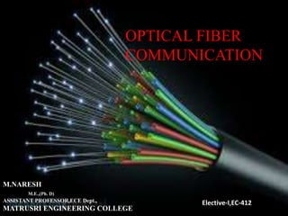
- 1. OPTICAL FIBER COMMUNICATION M.NARESH M.E.,(Ph. D) ASSISTANT PROFESSOR,ECE Dept., MATRUSRI ENGINEERING COLLEGE Elective-I,EC-412
- 2. UNIT-I • Evolution of fiber optic system • Elements of Optical Fiber Transmission link • Optical Fiber Modes and Configurations • Ray Optics • Mode theory of Circular Waveguides: -Overview of Modes and Key concepts - Linearly Polarized Modes • Single Mode Fibers and Graded Index fiber structure
- 3. Evolution of Fiber optic System(1/2): Circa 2500 B.C. Earliest known glass Roman times-glass drawn into fibers Venice Decorative Flowers made of glass fibers 1609-Galileo uses optical telescope 1626-Snell formulates law of refraction 1668-Newton invents reflection telescope 1840-Samuel Morse Invents Telegraph 1841-Daniel Colladon-Light guiding demonstrated in water jet 1870-Tyndall observes light guiding in a thin water jet 1873-Maxwell electromagnetic waves 1876-Elisha Gray and Alexander Bell Invent Telephone 1877-First Telephone Exchange 1880-Bell invents Photophone 1888-Hertz Confirms EM waves and relation to light 1880-1920 Glass rods used for illumination 1897-Rayleigh analyzes waveguide 1899-Marconi Radio Communication 1902-Marconi invention of radio detector 1910-1940 Vacuum Tubes invented and developed 1930-Lamb experiments with silica fiber 1931-Owens-Fiberglass 1936-1940 Communication using a waveguide 1876-Alexander Graham Bell 1876 First commercial Telephone 1970 I. Hayashi Semiconductor Laser
- 4. Evolution of Fiber optic System (2/2): 1951-Heel, Hopkins, Kapany image transmission using fiber bundles 1957-First Endoscope used in patient 1958-Goubau et. al. Experiments with the lens guide 1958-59 Kapany creates optical fiber with cladding 1960-Ted Maiman demonstrates first laser in Ruby 1960-Javan et. al. invents HeNe laser 1962-4 Groups simultaneously make first semiconductor lasers 1961-66 Kao, Snitzer et al conceive of low loss single mode fiber communications and develop theory 1970-First room temp. CW semiconductor laser-Hayashi & Panish April 1977-First fiber link with live telephone traffic- GTE Long Beach 6 Mb/s May 1977-First Bell system 45 mb/s links GaAs lasers 850nm Multimode -2dB/km loss Early 1980s-InGaAsP 1.3 µm Lasers - 0.5 dB/km, lower dispersion-Single mode Late 1980s-Single mode transmission at 1.55 µm -0.2 dB/km 1989-Erbium doped fiber amplifier 1 Q 1996-8 Channel WDM 4th Q 1996-16 Channel WDM 1Q 1998-40 Channel WDM
- 5. Bells Photophone 1880 - Photophone Transmitter 1880 - Photophone Receiver “The ordinary man…will find a little difficulty in comprehending how sunbeams are to be used. Does Prof. Bell intend to connect Boston and Cambridge…with a line of sunbeams hung on telegraph posts, and, if so, what diameter are the sunbeams to be…?…will it be necessary to insulate them against the weather…?…until (the public) sees a man going through the streets with a coil of No. 12 sunbeams on his shoulder, and suspending them from pole to pole, there will be a general feeling that there is something about Prof. Bell’s photophone which places a tremendous strain on human credulity.” New York Times Editorial, 30 August 1880
- 6. Approaches to Optical Communication
- 10. Operating ranges of components
- 11. Why fiber?
- 12. Elements of Optical Fiber Transmission link
- 16. Optical Fiber System(WDM) 2/2
- 17. Optical fiber cable installations
- 18. Spherical and plane wave fronts Nature of Light
- 19. Field distributions in plane E&M waves Adding two linearly polarized waves
- 21. Optical Fiber Modes and Configurations
- 23. Types: 1.step index 2. Graded index Mode: The propagation of light a long a wave guide can be described in terms of set of guided electromagnetic waves called “ Modes of the Waveguide” 1.The Refractive index of the Core is Uniform throughout and undergoes an abrupt change (step) at the cladding boundary is called “STEP-INDEX” 2. The Core Refractive index is made to vary as a function of the radial distance from the center of the fiber is called “ GRADED-INDEX” Both the step and graded-index fibers can be further dived into single and multimode Classes.
- 24. Comparison of single mode and multi-mode step index and graded index optical fiber
- 25. Ray optics Ray optics representation of skew rays travelling in a step –index fiber optical core Two types of rays: 1. Meridional rays 2. Skew rays Meridioanl rays confined to the meridian plan of the fiber, ray lines in a single plane, its path is Easy to track it travels along the fiber. It is two types 1.Bound rays 2. Trapped rays. Skew rays are not confined to a single plane, but instead tend to follow a helical –type path Along the fiber as. It is difficult to track. It constitute a major portion of the total no. of guided Rays.
- 26. Meridional ray representation Meridional ray optics for step –index fiber wave guide From the Snells law the min. critical angle SinØc= n2/n1
- 27. Light wave propagation Light wave propagation along a fiber waveguide. Phase changes occur both as the wave traveles Through the fiber medium an at the reflection points.
- 28. Mode theory of Circular Waveguides: -Overview of Modes and Key concepts - Linearly Polarized Modes To attain a more detailed understanding of the optical power propagation mechanism in Fiber, it is necessary to solve MAXWELL’s equations subject to the cylindrical boundary conditions at the interface between the core and cladding of the fiber. Key model concepts:
- 29. Single Mode Fibers and Graded Index fiber structure
- 30. Propagation modes in Single –Mode Fibers Two polarizations of the fundamental HE11 mode in a single- mode fiber
- 32. UNIT-II ATTENUATION & DISPERSION • Attenuation - Absorption losses - Scattering losses, - Bending Losses, - Core and Cladding losses • Signal Distortion in Optical Waveguides-Information Capacity determination - Group Delay - Material Dispersion - Waveguide Dispersion - Signal distortion in SM fibers Polarization Mode dispersion - Intermodal dispersion, • Pulse Broadening in Guided Index fibers, Mode Coupling • Design Optimization of Single Mode fibers-Refractive Index profile and cut-off wavelength
- 33. ATTENUATION • Signal Attenuation also known as ‘FIBER LOSS ‘ or ‘SIGNAL LOSS’. • Attenuation of a light signal as it propagation along a fiber is an important consideration in the design of optical communication system. • The Degree of Attenuation plays major role in determining the maximum transmission distance between a Transmitter and receiver. • The basic mechanism in a fiber are Absorption, Scattering, Radiative losses. • Absorption is related to FIBER MATERIAL. • Where as Scattering is associated both with the fiber material and with structural imperfections in the optical waveguide.
- 34. ATTENUATION UNITS: • As light travels along a fiber, its decreases exponentially with distance. If P(0) is the optical power in a fiber at the origin(at z=0),then the power P(z) at a distance z farther down the fiber is P(z) = P(0) e-αpz where ) ( ) 0 ( ln 1 z P P z p ) ( 343 . 4 ) ( ) 0 ( log 10 ) / ( 1 km z P P z km dB p Attenuation coefficient in units decibels per kilometer
- 35. Absorption • Absorption is caused by 3 different mechanisms: 1. Absorption by atomic defects in the glass composition 2. Extrinsic absorption by impurity atoms in the glass material 3. Intrinsic absorption by the basic constituent atoms of the fiber material. 1 rad(Si) = 100 erg/g = 0.01 J/Kg
- 36. Effects of ionizing radiation: a. Loss increase during steady irradiation to a total dose of 104 rad. b. Subsequent recovery as a function of time after radiation has stopped.
- 37. Optical fiber attenuation as a function of wavelength yields nominal values of 0.40db/km At 1310nm for standard single-mode fiber absorption by water molecules.
- 38. 63 . 4 exp 10 60 6 . 46 2 . 154 2 X x x uv 48 . 48 exp 10 81 . 7 11 X X IR
- 39. Optical fiber attenuation characteristics and their limiting mechanisms for aGeO2 doped low loss low water content silica fiber.
- 40. Scattering Loss (1/3) Scattering losses in glass arise from microscopic variations in the material in the Material density, fro compositional fluctuations, and from structural inhomogenetics Or defects occurring during fiber manufacture. Glass is composed of a randomly connected network of molecules. Such a structure naturally contains regions in which the molecular density is either higher or lower than average density in the glass. In addition , since glass is made of several oxides, such SiO2,Geo2, and P2O5, compositional fluctuations can occur. These 2 effects give rise to refractive index variations that occur within the glass over distances that are small compared with the wavelength. These index variations cause a Rayleigh-type scattering of the light. Rayleigh scattering in glass is the same phenomenon that scatters light from the sun n the atmosphere, there by giving rise to a blue sky. The expressions for scattering- induced attenuation are fairly complex owing to the random molecular nature and the various oxide constituents of glass. For single- component glass the scattering lost at wavelength ʎ resulting from density fluctuations can be approximately:
- 41. T f B scat T k n 2 2 4 3 ) 1 ( 3 8 Alternatively T f B scat T k p n 2 2 4 3 3 8 P is the photo elastic coefficient
- 44. Fundamental mode filed in a curved optical waveguide Bending losses: Radiative losses occur whenever an optical fiber undergoes a bend of finite radius Of curvature. Two types of curvatures: 1. Macroscopic bends having radii that are large compared with the fiber diameter such as those that occur when a fiber cable turns a corner. 2. Random Microscopic bens of the fiber axis that can arise when the fibers are incorporated into cables.
- 45. } ) 2 3 ( 2 2 2 1 { 3 / 2 2 kR n R a M Meff 2 1 ) ( 2 ka n M 2 4 2 1 ) ( j f M E E a b F
- 47. CORE AND CLADDING LOSSES Core and cladding have different indices of refraction and therefore differ in Composition, the core and cladding generally have different attenuation coefficients, denoted α1 and α2 rspectively. If the influence of modal coupling is ignored, the loss for a mode of order (v,m) for a step index v=waveguide is: p p p p clad core vm 2 1 p pcladd vm ) ( 1 2 1 The total loss of the waveguide can be found by summing over all modes weighted By the fractional power in that mode
- 48. SIGNAL DISPERSION IN FIBERS An optical signal weakens from attenuation mechanism And broadens due to Dispersion effects as it travels along a fiber. Eventually these two factors will cause neighboring pulses to overlap. After a certain amount of overlap occurs, the receiver can no longer distinguish the individual adjacent pulses and errors arise when interrupting the received signal
- 49. Overview of Dispersion Origins: Signal dispersion is a consequence of factors such as -Intermodal delay/Internalmodal dispersion - Intramodal Dispersion - Polarization – mode Dispersion - High –order Dispersion effects. Intermodal Delay appears only in multimode fibers. Intermodal Dispersion/Chromatic Dispersion is pulse spreading that takes place within a single mode. This spreading arises from the finite spectral emission width of an optical source. The phenomenon is also known as Group velocity Dispersion. The spectral width is the band of wavelength over which the source emits light. This wavelength band normally is characterized by the root-mean-square(rms) spectral widthσλ. Depending on the device structure of a light emitting diode(LED), the Spectral width is approximately 4 to 9 percent of a central wavelength. The two main causes of intermodal dispersion are as following: 1. Material dispersion 2. Waveguide dispersion
- 50. Polarization mode dispersion Polarization mode dispersion results from the fact that light-signal energy at a given wavelength in a single mode fiber actually occupies two orthogonally polarization states or modes. At the start of the fiber the two polarization states are aligned. However , since fiber material is not perfectly uniform throughout its length. The group Velocities of two orthogonal polarization modes are Vgx and Vgy, then the differential time delay during of the pulse over a distance L is gy gx PMD V L V L
- 51. MODAL DELAY (1/2) • Intermodal dispersion or Modal delay appears only in multi-mode fibers • This signal-distorting mechanism is a result of each mode having a different value of the group delay velocity at a single frequency. • The steeper the angle of propagation of the ray congruence, the higher is the mode number and consequently the slower the axial group velocity. This variation in the group velocities of the different modes results in a Group Delay spread, which is the intermodal Dispersion. • This dispersion mechanism is eliminated by single- mode operation but is important in multimode fibers. • The maximum pulse broadening arising from the modal delay is the difference between the travel time Tmax of the longest ay congruence paths and the travel time Tmin of the shortest ray congruence paths. • This broadening is simply obtained from ray tracing and for a fiber of length L is given by; c Ln cn Ln L L c n T T T c 1 2 2 1 1 min max sin
- 52. MODAL DELAY (2/2) Maximum Bit rate B can be sent over a multimode step-index fiber. Typically the fiber capacity is specified in terms of the “Bit rate- distance product (BL).” In order for neighboring signal pulses to remain distinguishable at the receiver , the pulse Spread should be less than 1/B, Which is the width of bit period. The bit rate – distance product: c n n BL 2 1 2 The rms impulse response s due to intermodal dispersion in a step-index Multimode fiber cane be c n NA L c Ln s 1 2 1 3 4 ) ( 3 2
- 53. Group Delay As the signal propagates along the fiber, each spectral component can be assumed to travel independently and to undergo a time delay/Group delay per unit length In the direction of propagation given by: dk d c dk d c V L g g 2 1 1 2 Group Velocity 1 1 d dk d c Vg Dispersion 2 2 1 1 c V d d d d L D g g
- 54. MATERIAL DISPERSION Material dispersion occurs because the index of refraction varies as a function of the optical wave length. To calculate material-induced dispersion , consider a plane wave propagating in the infinitely extended dielectric medium that has a refractive index n(λ) equal to the fiber core. Then the Propagation constant β is given by: ) ( 2 n Group delay from material Dispersion d dn n c L mat ) ( 2 2 mat mat mat D L d n d c L d d
- 55. WAVE GUIDE DISPERSION 2 2 2 1 2 2 2 2 2 1 n n n k V ua b For small values of the index difference Δ=(n1-n2)/n1 can be approximated by 2 1 2 n n n k b Where β ) 1 ( 2 b k n Waveguide dispersion is dk kb d n n c L dk d c L wg ) ( 2 2
- 56. CHARACTERISTICS OF SINGLE MODE FIBERS Refractive index profile configuration used to produce different fiber types Cutoff wavelength Dispersion calculations Mode field Diameter Bending loss
- 58. THREE DIMENSION AL REFRACTIVE INDEX PROFILES
- 61. CUTOFF WAVELENGTH The cutoff wavelength of the first higher –order mode (LP11) is an important transmission parameter for single mode fiber because it separated the single mode from the multi mode regions. Single mode operation occurs above the theoretical cutoff wavelength given by: 2 2 ) ( 2 1 2 / 1 2 2 2 1 n V a n n V a c P1(λ) is measured as a function of wavelength in sufficiently wide range around the expected cutoff wavelength. P2(λ) is measured over the same wavelength range when a loop of sufficiently small radius is included in the test fiber to filter the LP11 mode, ) ( ) ( log 10 ) ( 2 1 p p R The logarithmic Ration:
- 62. DISPERSION CALCULATIONS The total chromatic dispersion in single mode fibers consist mainly of material and the wave guide dispersion. The resultant intermodal or chromic dispersion is represented by: d d L D 1 ) ( The dispersion is commonly expressed in ps/(nm.km). The Broadening of σ of an optical pulse over a fiber of length L is given by: L D ) ( The Dispersion behavior varies with wavelength and also with fiber type The EIA and ITU-T have recommended different formulas to calculate the chromatic dispersion for specific fiber types operating in a given wavelength region. To calculate the dispersion for a non-dispersion shifted fiber in the 1270-to-1340nm region, The standards recommend fitting the measured group delay per unit length to three-term Sellmeier equation of the form: 2 2 C B A
- 63. 2 2 C B A A, B and C are the curve-fitting parameters, and equivalent expression is 2 2 0 0 0 8 S Whereλ0 is the relative delay min. at zero So is the value of the dispersion slope S(λ)=Dd/dλ at λo The Dispersion for a non-dispersion –shifted fiber is: 4 1 4 ) ( o o S D To calculate the dispersion for a dispersion-shifted fiber In the 1500-to-1600nm region, The standard recommended using the quadratic expression: 2 0 0 2 o S Which results in the dispersion expression o O S D ) ( ) (
- 64. Typical mode field diameter variations with wavelength for 1300 nm optimized, Dispersion shifted and Dispersion-flattened single-mode fibers MODE FIELD DIAMETER (MFD) In a single mode fibers the geometric distribution of light in the propagating mode is what is needed when predicting the performance characteristics of the these fibers. Thus a fundamental parameter of a single-mode fiber is mode field diameter. Since it takes into account the wavelength-dependent field penetration into the cladding.
- 65. Bending Loss: Macro bending and Micro bending losses are important in the design of single- mode fibers. These losses are principally evident in the 1550nm region and show up as a rapid increase attenuation when the fiber is bent smaller than a certain bend radius. The lower the cutoff wavelength relative to the operating wavelength, the more susceptible single-mode fiber are to bending.
- 66. The bending losses are primarily a function of the mode-field diameter. Generally the smaller the mode field diameter, the smaller the bending loss. This is true for the both matched-clad and depressed-clad fibers. Calculated increase in attenuation at 1310nm from micro bending and macro bending effects as a function of MFD (a) Depressed-cladding single mode fiber(V=2.514) (b) Matched-Cladding single-mode fiber(V=2.373). Micro bending calculations assume a correlation length Lc
- 67. Calculated Bend loss as a function of bend radius at 1300nm. The Dashed line represents the infinite- cladding case.i.e.,n2=n3 This example gives of calculated bend loss as a function of bend radius at a 1300nm wavelength. The fiber parameters were core radius a=3.6µm,cladding radius b=60µm, (n1-n2)/n2=3.56 X 10-3 and (n3-n2)/n2=0.07
- 69. UNIT-III OPTICAL SOURCES POWER LAUNCHING AND COUPLING Direct and indirect Band gap materials LED structures Light source materials, Quantum efficiency LED power, Modulation of LED, laser Diodes Modes and Threshold condition Rate equations, External Quantum efficiency Resonant frequencies, Laser Diodes, Temperature effects Introduction to Quantum laser, Fiber amplifiers Power Launching and coupling, Lensing schemes Fiber-to-Fiber joints, Fiber splicing
- 70. TOPICS FROM SEMI CONDUCTOR PHYSICS Pure-crystal energy-band diagram
- 71. n-type material
- 72. p-type material
- 73. A pn-junction
- 74. Reverse bias condition Forward bias condition
- 75. Direct and Indirect Band gaps:
- 76. Double-heterostructure configuration LIGHT –EMITTING DIODES (LEDs): 1. LED Structures:
- 79. 2.Light Source materials Semi conductor material Band gap energy (ev) Si 1.12 GaAs 1.43 Ge 0.67 Inp 1.35 Ga0.03Al0.03As 1.51 Band gap energies of some common semiconductor materials The semiconductor material that is used for the active layer of an optical sourc have a Direct band gap. In direct band gap semiconductor, electrons and holes can recombine directly the band gap without needing a 3rd particle to conserve momentum. The most important of these compounds are made from III-IV materials. III-Group: Al, Ga or In V-Group: P,As or Sb
- 81. The alloys GaAlAs and InGaAsP are chosen to make semiconductor light sources because it is possible to match the lattice parameters of the hetro-structure interfaces by using a proper combination of binary, ternary and quaternary materials. ---A very close match between the crystal lattice parameters of the two adjoining hetro-junctions is required to reduce interfacial detects and to minimize strain in the device as the temperature varies. ---These factors directly affect the radiative efficiently and life time of the light source. --Using the fundamental quantum-mechanical relationship between energy E and frequency v. hc hv E ) ( 240 . 1 ) ( ev E m g The peak emission wavelength λ in micrometers can be expressed as a function of the band gap energy Eg in electron volts by the equation
- 82. The relationships between the band gap energy Eg and the crystal lattice spacing ao for various III-V Compounds are plotted.
- 83. Typical spectral patterns for edge-emitting and surface-emitting LEDS at 1310nm. LED type Material Wavelength (nm) Operating current (mA) Fiber coupled power (µm) FWHM (nm) SLED GaAlAs 850 110 40 35 ELED InGaAsP 1310 100 15 80 SLED InGaAsP 1310 110 30 150 Typical characteristics of surface-and edge-emitting LEDs
- 84. Quantum Efficiency and LED power(1/4): t e n n 0 An excess of electrons and holes in p-type and n-type material created in a semiconductor light source by carrier injection at the device contacts. The excess carrier density decays exponentially with time according to the relation: The excess carriers can recombine either radiatively or non-radiativley. In radiative recombination a photon energy hv is emitted. In Non-radiative recombination effects optical obsorption in active region. when there is a constant current flow into a LED, an equilibrium condition is established. i.e., the excess density of e and holes is equal since the injected c are created and recombined in pairs such that charge neutrility is maintained i the device. The total rate at which carriers are generated is the sum of the externally supp The thermally generated rates.
- 85. Quantum Efficiency and LED power(2/4): n qd J dt dn qd J n nr t t R R R int The Externally supplied rate is given by J/qd, where d is thickness of recombination The thermal generation rate is given by n/г,Hence the rate equation for ca recombination in an LED can be written as: The equilibrium condition is found by setting above equation equal to zero: This relationship gives the steady-state electron density in the active region wh a constant is flowing though it. The internal quantum efficiency in the active region is the fraction of the electron-hole pairs that recombine radiatively: Rτ-radiative recombination rate, Rnτ-non radiative recobination rate
- 86. Quantum Efficiency and LED power(3/4): T nr r / 1 1 int q I R R nr / q hcl hv q I P out int int For exponential decay of excess carriers, the radiative recombination is R n r / Non-radiative recombination n nr R n / then the internal quantum efficiency can be expressed as: Where the bulk recombination life time τ is nr r 1 1 1 If the current injected into the LED is I, then the total number of recombination per second Substitute above equation in internal quantum efficiency then q I Rr int Noting Rr is the total no. of photons generated per second and that each photo energy hv, then the optical power generated internally to the LED is:
- 87. 2 ) 1 ( 1 n n ext 2 int int ) 1 ( n n p p P ext 2 2 1 2 1 ) ( 4 ) 0 ( n n n n T c d T ext 0 ) sin 2 )( ( 4 1 External quantum efficiency The external quantum efficiency can be calculated from the expression Where T(Φ) is the Fresnel transmission coefficient or Fresnel transmissivity this factor dep on there incidence angle Φ but for simplicity we can use the expression for the normal in Assuming the out side medium is air and letting n1=n2 then T(0)=4n/(n+1)2 ,the external quantum efficiency is Optical power emitted from the LED is Quantum Efficiency and LED power(4/4 Only light falling within a core defined by the critical angle Φc w be emitted from an optical source
- 88. Modulation of an LED(1/3): The response time or frequency response of an optical source dictates how fast an electrical input drive signal can vary the light output level. Following 3 factors largely determine the response time: 1. Doping level in the active region 2. Injected carrier life time гi in the recombination region 3. parasitic capacitance of the LED. If the drive current is modulated at a frequency w, the optical output power of the device ill vary as 2 1 2 0 ) ( 1 ) ( i P P Where Po is the power emitted at zero modulation frequency. The modulation bandwidth of LED can be defined in either in electrical or optical t
- 89. Modulation of an LED(2/3): Frequency response of an optical source showing the electrical and optical 3-dB bandwidth points An optical source exhibits a linear relationship between light power and current, so currents rather than voltages are compared in optical systems.
- 90. Modulation of an LED(3/3): P(w)=I2 (w)/R the ratio of the output electrical power at the frequency w to the power at zero modulation is ) 0 ( ) ( log 10 ) 0 ( ) ( log 10 2 2 I I p p Ratioelec Where I(w) is the electrical current in the detection circuitry. the electrical 3-dB points occurs at that frequency point where the detected electrical power P(w)= That happens when 2 1 ) 0 ( ) ( 2 2 I I Or I(w)/I(0)=1/√2=0.707 Some times, the modulation BW of an LED is given in terms of the 3-dB BW of the Modulated optical power P(w),at that frequency p(w)=Po/2.The 3-dB BW is determined From the ratio of the optical power at frequency w to the un-modulated value of the optic Power. Since the detected current is directly proportional to the optical power, the ratio is ) 0 ( ) ( log 10 ) 0 ( ) ( log 10 I I p p Ratiooptical
- 91. LASER DIODES Lasers come in many forms with dimensions ranging from the size of A grain of salt to one that will occupy an entire room. The lasing medium can be Gas, liquid, an insulating crystal(solid state), a semiconductor. Despite their differences, the basic principle of operation is the same for each type of Laser action is the result of three key processes. Photon absorption, Spontaneous emission, and Stimulated emission. These three processes are represented by the simple two-energy diagrams.
- 92. Laser transition processes E1 is the ground state energy and E2 is the excited-state energy. According to the planck’s law: a transition between these two states involves the absorption or emission of photon of energy hv12=E2-E1. E2 is the unstable state, the electron will shortly return to the ground state, there by emitting a photon of energy hv12, this occurs without and external stimulation and is called spontaneous emission. The electron can also be induced to make a down ward transition from the
- 93. LASER diode Modes and Threshold conditions Fabry-Perot resonator cavity
- 94. havior of the resonant wavelength in a Fabry- perot cavity for 3 values of the mirror reflectivity
- 95. DFB laser
- 96. Optical output vs. drive current At low diode currents, only spontaneous radiation is emitted. Both the spectral range and the lateral beam width of this emission are broad like that of an LED. A Dramatic and sharply defined increase in the power o/p occurs at the lasing threshold. The threshold current Ith is conventionally defined by extrapolation of the lasing region of the power-versus-current curve. At high power o/p the slope of the curve decreases because of
- 97. Laser Diode Rate Equations: The relationship between optical output power and the diode drive current can be determined by examining the rate equations that govern the interaction of photon and electrons in the active region. The total carrier population is determined by carrier injection, spontaneous recombination and stimulated emission. For a pn junction with a carrier – confinement region of depth d , the rate equation ph sp R Cn dt d =stimulated emission +spontaneous emission + Photon loss Cn n qd J dt dn sp Which governs the no. of photons ‘Ø’ =injection + spontaneous recombination + stimulated emission Which governs the no. of electrons ‘n’ C-coefficient describing the strength of the optical absorption and emission interactions Rsp- rate spontaneous emission into the lasing mode τph- photon life time, τsp- spontaneous recombination life time J-is the injection-current density
- 98. 0 1 ph n C qd J t n th sp th ph s sp s th R Cn 0 s th sp th Cn n qd J 0 sp ph th ph s R J J qd ) ( The steady state is characterized by the left-hand sides of above equation being equa First ,assuming Rsp is negligible and noting that dφ/dt must be positive when φis small,t This shows that n must exceed a threshold value nth in order for φ to increase. This threshold value can be expressed in terms of the threshold current Jth need to main An inversion level n=nth in the steady state when no.of photos φ=0 This expression defines the current required to sustain an excess electron density in the la When spontaneous emission is the only decay mechanism. Consider the photon and elect equations in the steady –state condition at the lasing threshold. and Φs-steady state photon density Adding above two equations using for the term nth/τsp, and solving for Φs Yields the no. of photons per unit volume:
- 99. External Quantum Efficiency: th th i ext g g ) ( ) ( ) ( ) ( 8065 . 0 mA dI mW dP m dI dP E q g ext External differential quantum efficiency is defined as the no. of photons emitted per radiative electron-hole pair recombination above threshold. Gain co-efficient remains fixed at gth Where , ηi-internal quantum efficiency This is not a well defined quantity in laser diodes, but most measurements Show that ηi≈0.6-0.7 at room temperature. Experimentally ext. Quantum efficiency is calculated from the straight, line portion of the curve for the emitted optical power P versus drive current I. Where Eg-band gap energy dP-incremental change in emitted optical pow dI-Drive current λ-emisssion wavelength
- 100. Resonant Frequencies: m L 2 2 / 2 n v c Ln n L m 2 2 / 2 2 0 2 ) ( exp ) 0 ( ) ( g g Let us examine the resonant frequencies of the laser m is an integer, using for the propagation constant Where c=vλ This states that the cavity resonates when an integer number m of half-wavelengths spans the region between the mirrors Some lasers are single-mode and some are multi-mode. The relation ship between gain and frequency can be assumed to have the Gaussian form: Where λo-wavelength at the center of the spectrum σ - spectral width of the gain g(o)-max. gain proportional to the population inversion
- 101. 1 2 1 m v c Ln m m v c Ln m 2 v c Ln v v c Ln m m 2 ) ( 2 1 1 Ln c v 2 Ln 2 2 This can be related to the wavelength spacing Δλ through the relationship Δv/v=Δλ/λ From which we have the frequency spacing Subtracting these two equations yields and Here, we consider only the longitudinal modes. Note ,however, that for each longitudina there may be several transverse modes that arise from one or more reflections of the propagating wave at the sides of the resonator cavity. consider two successive modes of frequencies vm-1 and vm represented by the integer m-1 and m.
- 102. Fabry-Perot GaAlAs/GaAs laser diode spectrum The output spectrum laser follows the typical gain-versus-frequency plot Where the exact no. of modes , their heights ,and their spacing's depend on the laser con
- 103. Laser Diode Structures and Radiation Patterns: A basic requirement for efficient operation of laser diodes is that, in addition to transverse optical confinement and carrier confinement between hetro-junction layers, the current flow must be restricted laterally to a narrow stripe along the length of the laser. Numerous novel methods of achieving this, with varying degrees of success, have been proposed, but all strive for the same goals of limiting the number of lateral modes so that lasing is confined to a single filament, stabilizing the lateral gain, and ensuring a relatively low threshold current. Dielectric waveguide materials are fabricated in the lateral direction. The variations in the real refractive index of the various materials in these structures control the lateral modes in the laser. These devices are called index-guided lasers. If a particular index-guided laser supports only the fundamental transverse mode and the fundamental longitudinal mode, is known as a single-mode laser. Index-guided lasers; (a) Positive –index waveguide (b) Negative-index waveguide In positive index- waveguide the central region has a higher refractive index than the outer regions. These lasers are more popular.
- 104. 3 Fundamental structures for confining optical waves in the lateral direction (a) In the gain – induced guide, electrons injected via a metallic stripe contact alter the Index of refraction of the active later (b) The positive index waveguide has a higher refractive index in the central portion of the active region (c ) The negative – index waveguide has a lower refractive index in the central portion of
- 105. Short-wavelength (800-900nm) GaAlAs Long-wavelength (1300-1600nm) InGaAsP To make the buried hetrostructure (BH) LASER, one etches a narrow mesa stripe (1- 2μm wide) in double- hetro structure material. The mesa is then embedded in high-resistivity lattice- matched n-type material with an appropriate band gap and low refractive index. A no. of variations of this fundamental structure have been used to fabricate high- performing laser diodes.
- 106. (a) Selectively diffused (b) Varying –thickness (c ) bent- la Positive –index Optical –wave-confining structure Index- guided lasers can be made using any one f four fundamental structures. These are the buried hetro-structure, a selectively diffused construction, a varying Thickness structure and a bent-layer configuration.
- 107. 4 Basic methods for achieving current confinement in laser diodes: Inner-stripe confinement Regrowth of back-biased pn junctions In addition to confining the optical wave to a narrow lateral stripe to achieve continuous high optical output power, one also needs to restrict the drive current tightly to the active layer so more than 60% of the current contributes to lasing.
- 108. Energy-band diagram for a quantum layer in a multiple quantum-well laser
- 109. Single-Mode Lasers: Basic Architecture of a vertical- cavity surface-emitting laser high-speed long-distance communications one needs single-mode lasers, which must contain only a single longitudinal mode and a single transverse mode. Consequently, the width of the optical emission is very narrow.
- 110. 3 types of Laser structures using built-in frequency selective resonator grat 1.Distributed- feed back (DFB) Laser 2. Distributed –Bragg reflector(DBR) Laser 3. Distributed- reflector (DR) Laser
- 111. Output spectrum symmetrically distributed around λB in an idealized distributed feedbac
- 112. Modulation of Laser Diodes:
- 114. External modulation
- 115. Temperature Effects: An important factor to consider in the application of laser diodes is the temperature depen of The threshold current Ith(T). This parameter increases with temperature in all types of semiconductor lasers because various Temperature-dependent factors. The complexity of these factors prevents the formulation of a single equation that holds For all devices and temperature ranges. 0 ) ( T T z th e I T I To-threshold temp. Iz - constant For GaAlAs laser diode To is 120-1650 C For GaAlAs quantum –well laser diode To is 4370 C
- 116. In the example given above , the threshold current increases by a factor of about 1.4 between 20 and 60 degree centigrade. In addition , the lasing threshold can change as the laser ages. Consequently , if a constant optical output power level is to be maintained as the temp. of the laser changes or as the laser ages, it is necessary to adjust the dc-bias current level. One possible method for achieving this automatically is an optical feedback scheme. Optical feed back can be carried out by using a photo detector either to sense the variation In optical power emitted from the rear facet of the laser or to tap off and monitor a small portion of the fiber coupled power emitted from the facet. photo detector compares the optical power output with a reference level and adjusts the dc- bias current level automatically to maintain a constant peak light output relative to
- 117. Standard method of stabilizing the optical output of a laser diode is to use a miniature thermoelectric cooler. This device maintains the laser at a constant temperature and thus stabilizes the output Normally a thermoelectric cooler is used in conjunction with a rear-facer detector feed ba loop.
- 118. PART-II Power Launching and coupling Lensing schemes Fiber-to-Fiber joints Fiber splicing In implementing an optical fiber link, two of the major system operations are 1.how to launch optical power into a particular fiber form some type of luminescent source and 2. how to couple optical from one fiber into another.
- 119. Launching optical power form a source into a fiber entails considerations Such as: Numerical apertarture, Core size Refractive –index profiles Core –cladding index difference of the fiber Size Radiance Angular power distribution of optical source A measure of the amount of optical power from a source that can be coupled into A fiber is usually given by the coupling efficiency η defined as S F P P F P Power coupled into the fiber Ps- power emitted from the light source The launching or coupling efficiency depends on the type of fiber that Is attached to the source and on the coupling process;
- 120. SOURCE TO FIBER POWER LAUNCHING A convenient and useful measure of the optical output of a luminescent source is its rad (or brightness) B at a given diode drive current. Radiance is the optical power radiated into a unit solid angle per unit emitting surface ar Is generally specified interims of watts per square centimeter per steradian; Since power that can be coupled into a fiber depends on the raidance, the Raidance of optical source than the total output is the important parameter When considering source-to-fiber coupling efficiencies. Spherical coordinate system For characterizing the Emission pattern From An optical source R,Ө,and Ø spherical coordinat system
- 121. Surface-emitting LEDs are characterized by their lambertian output pattern. The power delivered at an angle Ө,measured relative to a normal to the emitting surface, v cos Ө because the projected area of the emitting surface varies as cos Ө with viewing dir The emission pattern for a lambertian source thus follows the relationship: Radiance patterns for a lambertian Source and the lateral output of a highly Directional laser diode, Both sources have Bo normalized to unity B(Ө,Ø) = Bo cos Ө Bo-radiance along the Normal to the radiating surface
- 122. Power coupling calculation Schematic diagram of a light source coupled to an optical fiber. Light outside of the acceptance angle is lost ) , ( s s s A s s f A B d dA p The coupled power can be found using the relationship s sand A are the area and solid emission angle of the source a forr NA P P s s Step LED 2 ) ( , 2 ) 0 ( 2 2 2 2 2 2 1 2 2 , NA B a n B a P o o Graded LED For step-index fiber: For graded-index fiber: 0 2 2 B r P s s Where
- 123. POWER LAUNCHING VERSUS WAVELENGTH Optical power launched into a fiber does not depend on the wavelength Of the source but only on its brightness: i.e., Radiance. 2 0 B M P S The no. of modes that can propagate in a multimode graded-index fiber Of core size a and index profile α is: 2 1 2 2 an M
- 124. LENSING SCHEMES If source-emitting area is larger than the fiber –core area, then the resulting Optical power coupled in to the fiber is the maximum that can be achieved . This is the result of fundamental energy and radiance conservation principle(also know as law of brightness).the emitting area However, if the emitting area of the source is smaller than the core , a miniature lens may be placed between the source and the fiber to improve the power-coupling efficiency. The function of the micro-lens is to magnify the emitting area of the source to match the core area of the fiber end face exactly. If the emitting area is increased by a magnification factor M, The solid angle within which optical power is coupled to the fiber form the source is increased by the same factor. These techniques can improve the efficiency, they also create additional complexities.
- 125. Examples of possible lensing schemes used to improve optical source-to- Fiber coupling efficiency
- 126. Nonimaging Microshere: One of the most efficient lensing method The focal point can be found from the Gaussian lens formula r n n q n s n ' ' 2 2 2 s L s L r R r R M Placing the LED close to the lens surface thus results in a magnification M of the emitting area. This is given by the ratio of the cross-sectional area of the lens to That of the emitting area:
- 127. Theoretical coupling efficiency in units Of (NA)2 for a surface – emitting LED as a function Of the light emitting diameter, coupling is to A fiber with a core radius a =25µm The optical power PL that can be coupled into a full aparture angle 2Ө is given by: 2 2 sin s L S L r R P P The theoretical coupling efficiency 1 ) ( 1 ) ( { 2 2 2 max a r for NA a r for NA r a s s s
- 128. FIBER-TO-FIBER JOINTS (1/4) A significant factor in any fiber optic system installation is the requirement to Interconnect fibers in a low loss manner. These interconnects occur at the optical source, at the photo-detector at the intermediate points with in a cable where two fibers are joined. The particular technique selected for joining the fibers depends on whether a permanent bond or an easily demountable connection is desired. A permanent bond is generally referred to as a splice, where as a demountable joint is known as “a connector”. Every joining technique is subject to certain conditions that can cause various amounts of Optical power loss at the joint. The loss at a particular junction or thought a component is Called the insertion loss.
- 129. Different modal distributions of the optical beam emerging from a fiber result in different degrees of coupling loss. (a) When all modes are equally excited, the output beam fills the entire output NA (b) for a steady-state modal distribution, only the equilibrium NA is filled by the output beam
- 130. Mechanical Misalignment: Three types of mechanical misalignments that can occur between two joints fi Mechanical alignment is a major problem when joining two fibers, owing to their Microscopic size. A standard multimode graded-index fiber core is 50-100µm in diameter, which is roughly the Thickness of the human hair.
- 131. Axial offset reduces the shaded common core area of the two fiber end faces Axial displacement results when the of the two fibers are separated by a Distance d. Longitudinal separation occurs when the fibers have the same Axis but have a gap s between their end faces.
- 132. Output power loss effect when fiber ends are separated longitudinally by
- 133. Experimental comparison of loss(in dB) as a function of mechanical misalignm
- 134. Fiber End-Face Preparation: Two examples of Improperly cleaved Fiber ends: Controlled-fracture procedure for fiber end preparation One of the firs steps that must be followed before fibers are connected or Spliced to each other is to prepare the fiber end faces properly. In order not to have light deflected or scatted at the joint, the fiber ends must be flat, perpendicular to the fiber axis, and smooth. End preparation techniques that have been extensively used include sawing, grinding and polishing, controlled fracture, and laser cleaving.
- 135. FIBER SPLICING: A Fiber splicing is a permanent or semi-permanant joint between two fibers These are typically used to create long optical links or in situations where frequent conn and Disconnections are not needed. In making and evaluting such splices, one must take into account the geometrical differe In the two fibers 1. Fiber mis-alignments at the joint 2. mechanical strength of the splice Fiber splicing techniques: 1. Fusion spice 2. V-groove mechanical splice 3. Elastic- tube splice
- 136. Fusion splicing of optical fibers V-groove of optical fibers splicing Elastic –tube splice
- 137. Splicing single-mode fibers: In single-mode fibers the lateral (axial) offset misalignment present the Most serous loss. This loss depends on the shape of the propagating mode. For Gaussian Shaped beams the loss between identical fibers is: } log{exp 10 2 . w d L lat SM Where w-spot size mode-field radius, d-lateral displacem For a gap s with a material of index n3, and letting G=s/kw2 ,the gap loss for identical single-mode fiber splices is: ) 4 ( ) ( 64 log 10 2 4 2 1 2 3 2 1 , G n n n n L gap SM
- 138. Connector Return loss Model of an index-matched connection with perpendicular fiber end faces
- 139. Connection with angled end faces having a small gap of width a separating the finer end
- 140. Reference Text Books
- 141. OPTICAL FIBER COMMUNICATION UNIT-IV PHOTO DETECTORS , OPTICAL RECIEVER OPERATION
- 142. CONTENTS • PIN and APD diodes, • Photo detector noise • SNR • Detector Response time • Avalanche Multiplication Noise • Comparison of Photo detectors • Fundamental Receiver Operation, preamplifiers • Error Sources, Receiver Configuration • Probability of Error • Quantum Limit
- 145. Quality Factors • Responsivity – Ratio of photons incident to current produced • Quantum Efficiency – Ratio of photons incident to EHP produced • Capacitance • Gain-Bandwidth Product – FWHM, rise time, fall time • Noise – Signal-to-noise ratio
- 146. Detector Technologies MSM (Metal Semiconductor Metal) PIN APD Waveguide Contact InP p 1x10¹⁸ Multiplication InP n 5x10¹⁶ Transition InGaAsP n 1x10¹⁶ Absorption InGaAs n 5x10¹⁴ Contact InP n 1x10¹⁸ Substrate InP Semi insulating Semiinsulating GaAs Contact InGaAsP p 5x10¹⁸ Absorption InGaAs n- 5x10¹⁴ Contact InP n 1x10¹⁹ Absorption Layer Guide Layers Simple, Planar, Low Capacitance Low Quantum Efficiency Trade-off Between Quantum efficiency and Speed High efficiency High speed Difficult to couple int Gain-Bandwidth: 120GHz Low Noise Difficult to make Complex Key: Absorption Layer Contact layers Layer Structure Features
- 147. Photo Detection Principles Device Layer Structure Band Diagram showing carrier movement in E-field Light intensity as a function of distance below the surface Carriers absorbed here must diffuse to the intrinsic layer before they recombine if they are to contribute to the photocurrent. Slow diffusion can lead to slow “tails” in the temporal response. Bias voltage usually needed to fully deplete the intrinsic “I” region for high speed operation
- 148. PIN Photodiodes • Large absorption area • Simple fabrication • Unity gain • Speed dependent on width • Thermally generated carriers create noise within region
- 149. PIN Photo diodes
- 150. PIN photodiodes Energy-band diagram p-n junction Electrical Circuit
- 151. PIN PHOTO DETECTOR Photons with energies greater Than or equal to the band gap Energy Eg can generate free Electron-hole pairs that act as Photocurrent carries
- 152. Characteristics of Photo-detectors Number of Collected electrons 1 Number of Photons *Entering* detector / Number of Collected electrons 1 1 Number of Photons *Incident* on detector / Photo Current (Amps) W i ph W e p o e i q R e P h R 1 1 Incident Optical Power (Watts) 1 1 ph o ph W p o W p o i RP i q R e P h R e P q h • Internal Quantum Efficiency •External Quantum efficiency • Responsivity •Photocurrent Incident Photon Flux (#/sec) Fraction Transmitted into Detector Fraction absorbed in detection region
- 153. Detector Sensitivity vs. Wavelength Absorption coefficient vs. Wavelength for several materials (Bowers 1987) Photodiode Responsivity vs. Wavelength for various materials (Albrecht et al 1986)
- 154. Comparison of responsivity and quantum efficiency
- 155. Avalanche Photodiodes • High gain due to avalanche multiplication effect • Increased noise • Silicon has high gain but low noise • Si-InGaAs APD often used(diagram on right) • High resistivity p-doped layer increases electric field across absorbing region • High-energy electron-hole pairs ionize other sites to multiply the current • Leads to greater sensitivity n + p + p i Electric field Depletion region
- 156. APD Detectors Signal Current s q i M P h APD Structure and field distribution (Albrecht 1986)
- 159. 2. PHOTO DETECTOR NOISE: L B L D p N R TB k B qI B M F M I I q i / 4 2 2 ) ( 2 2
- 161. Signal to Noise Ratio ip= average signal photocurrent level based on modulation index m iD=dropped current L B L D p p R TB k B qI B M F M I I q M i N S / 4 2 2 2 2 2 L e B e p p R TB k B M F M qI i M N S / 4 ) ( 2 ) ( / 2 2 2
- 162. Reverse-biased pin photodiode Photo diode not fully deployed Rise and Fall times 4. DETECTOR RESPONSE TIME:
- 163. Photo diode pulse responses under Various detector parameters The response time of photo detector together with its output circuit depends mainly on the following 3 factors 1. The transit time of photo carriers in the depletion region 2. The diffusion time of the photo carriers generated outside the depletion region 3. The RC time constant of the photodiode and its associated circuit td= w/vd
- 164. Typical Characteristics of P-I-N and Avalanche photodiodes or comparison of Photo-detectors
- 165. Comparisons • PIN gives higher bandwidth and bit rate • APD gives higher sensitivity • Si works only up to 1100 nm; InGaAs up to 1700, Ge up to 1800 • InGaAs has higher for PIN, but Ge has higher M for APD • InGaAs has lower dark current
- 166. Fundamental Receiver Operation Signal path through an optical data link
- 167. Receiver Functional Block Diagram
- 168. Error Sources: NOISE SOURCES Internal: Switch and power supply transients External: Electric power lines, motors, radio transmitters, lightning Short noise arises in electronic devices because of the discrete nature of current flow in the device. Thermal noise arises from the random motion of electrons in a conductor
- 170. Digital Receiver performance In digital receiver the decision-circuit output signal voltage Vout(t) would always exceed the threshold voltage When a “1” is present and would be less than the threshold when “o” pulse was sent. In actual system, deviations from the average value are caused by various noises, interfaces from adjacent pulses and conditions where in the light source is not completely extinguished during a zero pulse Probability of Error Quantum Limit Bt N N N BER e t e Probability of Error: A simple approach is to divide the no. of errors occurring over certain time interval t by the no. of pulses . Where B=1/Tb is the bit rate
- 171. Probability distribution for received logic 0 and logic 1 Signal pulses. The different widths Of the two distributions are caused By various signal distortion effect. Gaussian noise statistics Of a binary signal Showing Variances around the ON and OFF signal levels
- 172. 2 / 2 1 ) ( Q x e dx e Q P BER Q e Q erf Q / 2 1 2 1 2 1 2 / 2
- 173. BER versus Q factor BER vs SNR
- 174. QUANTUM LIMIT In designing an optical system, it is useful to know what the fundamental physical bounds are on the system performance. Suppose we have a ideal photo detector that has a unity quantum efficiency and produces No dark current, i.e., no electron – hole pairs are generated in the absence of an optical pulse. In the given above condition to finding the min. received optical power required for Specific bit-error rare performance in the digital system. This min. received power level is know as the “QUANTUM LIMIT” N r e P ) 0 ( Error Probability N- avg. no. of electron-hole pairs E-min. optical pulse energy Ƭ-photo detector time intervel
- 175. Thank you
Editor's Notes
- 2
- 1
- 6
- 4
- 1
- 2
- 6
- 2
- 1
- 3
- 5
- 6
- 7
- 8
- 1
- 2
- 3
- 4
- 5
- 7