2. forces).1
We will observe first how these forces encouraged/discouraged
the development of piezoelectric materials.
1.1.1 The Dawn of Piezoelectrics
The Curie brothers (Pierre and Jacques Curie) discovered direct piezo-
electric effect in single crystal quartz in 1880. Under pressure, quartz gen-
erated electrical charge/voltage from quartz and other materials. The root
of the word “piezo” means “pressure” in Greek; hence the original mean-
ing of the word piezoelectricity implied “pressure electricity.” Materials
showing this phenomenon also conversely have a geometric strain pro-
portional to an applied electric field. This is the converse piezoelectric effect,
discovered by Gabriel Lippmann in 1881. Recognizing the connection
between the two phenomena helped Pierre Curie to develop pioneering
ideas about the fundamental role of symmetry in the laws of physics.
Meanwhile, the Curie brothers put their discovery to practical use by
devising the piezoelectric quartz electrometer, which could measure faint
electric currents; this helped Pierre’s wife, Marie Curie, 20 years later in
her early research.
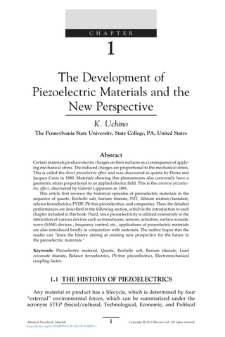
It was at 11:45 pm on Apr. 10, 1912 that the tragedy of the sinking of the
Titanic occurred (see Fig. 1.1). As the reader knows well, this was caused
by an iceberg hidden in the sea. This would have been prevented if the
ultrasonic sonar system had been developed then. Owing to this tragic
incident (social force), there was motivation to develop ultrasonic technol-
ogy development using piezoelectricity.
FIG. 1.1 The sinking of the Titanic was caused by an “iceberg” in the sea.
2 1. THE DEVELOPMENT OF PIEZOELECTRIC MATERIALS AND THE NEW PERSPECTIVE
3. 1.1.2 World War I—Underwater Acoustic Devices
With Quartz and Rochelle Salt
The outbreak of World War I in 1914 led to real investment to accelerate
the development of ultrasonic technology in order to search for German
U-Boats under the sea. The strongest forces both in these developments
were social and political. Dr. Paul Langevin, a professor at Ecole
Sup
erieure de Physique et de Chimie Industrielles de la Ville de Paris
(ESPCI Paris Tech), who had many friends including Drs. Albert Einstein,
Pierre Curie, Ernest Ratherford, among others, started experiments on
ultrasonic signal transmission into the sea, in collaboration with the
French Navy. Langevin succeeded in transmitting an ultrasonic pulse into
the sea off the coast of southern France in 1917. We can learn most of the
practical development approaches from this original transducer design
(Fig. 1.2). First, 40 kHz was chosen for the sound wave frequency. Increas-
ing the frequency (shorter wavelength) leads to better monitoring resolu-
tion of the objective; however, it also leads to a rapid decrease in the
reachable distance. Notice that quartz and Rochelle salt single crystals
were the only available piezoelectric materials in the early 20th century.
Since the sound velocity in quartz is about 5 km/s, 40 kHz corresponds
to the wavelength of 12.5 cm in quartz. If we use a mechanical resonance
in the piezoelectric material, a 12.5/2¼6.25 cm thick quartz single crystal
piece is required. However, in that period, it was not possible to produce
such large high-quality single crystals.2
1.0
28.7
28.7
260 mm f
5.0
0.5
0.5
Steel
Center axis
Angle
dependence
of
acoustic
power
Quartz pellets
were arranged
FIG. 1.2 Original design of the Langevin underwater transducer and its acoustic power
directivity.
3
1.1 THE HISTORY OF PIEZOELECTRICS
4. In order to overcome this dilemma, Langevin invented a new trans-
ducer construction; small quartz crystals arranged in a mosaic were sand-
wiched by two steel plates. Since the sound velocity in steel is in a similar
range to quartz, with 6.25 cm in total thickness, he succeeded to set the
thickness resonance frequency around 40 kHz. This sandwich structure
is called Langevin type and remains popular even today. Notice that quartz
is located at the center, which corresponds to the nodal plane of the thick-
ness vibration mode, where the maximum stress/strain (or the minimum
displacement) is generated in the resonance mode.
Further, in order to provide a sharp directivity for the sound wave, Lan-
gevin used a sound radiation surface with a diameter of 26 cm (more than
double of the wavelength). The half-maximum-power angle ϕ can be eval-
uated as
ϕ ¼ 30 λ=2a
ð Þ degree
, (1.1)
where λ is the wavelength in the transmission medium (not in steel) and a is
the radiation surface radius. If we use λ¼1500(m/s)/40(kHz)¼3.75 cm,
a¼13 cm, we obtain ϕ¼4.3 degree for this original design. He succeeded
practically in detecting the U-Boat 3000 m away. Moreover, Langevin also
observed many bubbles generated during his experiments, which seems to
be the “cavitation” effect that was utilized for ultrasonic cleaning systems
some 60 years later.
Though the mechanical quality factor is significantly high (i.e., low loss)
in quartz, its major problems for this transducer application include its
low electromechanical coupling k, resulting in (1) low mechanical under-
water transmitting power and receiving capability, and in (2) narrow fre-
quency bandwidth, in addition to the practical fact that only Brazil
produced natural quartz crystals at that time. Thus, US researchers
used Rochelle salt single crystals, which have a superior electromechanical
coupling factor (k is close to 100% at 24°C!) with a simple synthesizing
process. Nicholson,3
Anderson, and Cady undertook research on the pie-
zoelectric underwater transducers during World War I. General Electric
Laboratory (Moore4
) and Brush Company produced large quantities of
crystals in the early 1920s. The detailed history on Rochelle salt can be
found in Ref. 5.
Rochelle salt is sodium potassium tartrate [NaKC4H4O64H2O], and it
has two Curie temperatures at 18°C and 24°C with a narrow operating
temperature range for exhibiting ferroelectricity; this leads to high electro-
mechanical coupling at 24°C and, however, rather large temperature
dependence of the performance. It was used worldwide for underwater
transducer applications until barium titanate and lead zirconate titanate
(PZT) were discovered. Since this crystal is water-soluble, it is inevitable
that it is degraded by humidity. However, the most delicate problem is its
weakness to dryness. Thus, no researcher was able to invent the best coating
technology for the Rochelle salt devices to achieve the required lifetime.
Many efforts to discover alternative piezoelectrics of Rochelle salt with
better stability/reliability continued after WWI. Potassium dihydrogen
4 1. THE DEVELOPMENT OF PIEZOELECTRIC MATERIALS AND THE NEW PERSPECTIVE
5. phosphase (KH2PO4 or KDP) was discovered by Georg Busch in 1935.6
Knowing the ferroelectricity of Rochelle salt, and guessing the origin to be
from the hydrogen bonds in the crystal, Busch searched hydrogen bond crys-
tals systematically and found KDP as a new ferroelectric/piezoelectric.
Though many piezoelectric materials (such as Rochelle salt, barium titanate,
and PVDF) were discovered accidentally through “serendipity,” KDP is an
exceptional example of discovery created by the perfectly planned systematic
approach. Following KDP, ADP, EDT, and DKT, amongst others, were dis-
covered continuously and examined. However, most of the water-soluble
single crystal materials have been forgotten because of the performance and
preparation improvements in synthetic quartz and perovskite ceramics
(BT, PZT).
1.1.3 World War II—Discovery of Barium Titanate
Barium titanate (BaTiO3, BT) ceramics were discovered independently
by three countries, the United States, Japan, and Russia, during World
War II: Wainer and Salomon7
in 1942, Ogawa8
in 1944, and Vul9
in
1944, respectively. Compact radar system development required compact
high capacitance “condensers” (the term “condenser,” rather than “capac-
itor,” was used at that time). Based on the widely used “Titacon” (titania
condenser) composed of TiO2-MgO, researchers doped various oxides to
find higher permittivity materials. According to the memorial article
authored by Ogawa and Waku,10
they investigated three dopants, CaO,
SrO, and BaO, in a wide fraction range. They found a maximum permit-
tivity around the compositions CaTiO3, SrTiO3, and BaTiO3 (all were iden-
tified as perovskite structures). In particular, the permittivity, higher than
1000, in BaTiO3 was enormous (10 times higher than that in Titacon) at that
time, as illustrated in Fig. 1.3.
BaO
1000
800
600
400
200
BaTiO3
TiO2
MgO
( %)
FIG. 1.3 Permittivity contour map on the MgO-TiO2-BaO system, and the patent coverage
composition range (dashed line).10
5
1.1 THE HISTORY OF PIEZOELECTRICS
6. It should be pointed out that the original discovery of BaTiO3 was not
related with piezoelectric properties. Equally important are the indepen-
dent discoveries by R. B. Gray at Erie Resister (patent applied for in 1946)11
and by Shepard Roberts at MIT (published in 1947)12
that the electrically
poled BT exhibited “piezoelectricity” owing to the domain realignment.
At that time, researchers were arguing that the randomly oriented “poly-
crystalline” sample should not exhibit piezoelectricity, but the secondary
effect, “electrostriction.” In this sense, Gray is the “father of piezocera-
mics,” since he was the first to verify that the polycrystalline BT exhibited
piezoelectricity once it was electrically poled.
The ease in composition selection and in manufacturability of BT
ceramics prompted Mason13
and others to study the transducer appli-
cations with these electroceramics. Piezoelectric BT ceramics had a reason-
ably high coupling coefficient and nonwater solubility, but the bottlenecks
were (1) a large temperature coefficient of electromechanical parameters
because of the second phase transition (from tetragonal to rhombohedral)
around the room temperature or operating temperature, and (2) the aging
effect due to the low Curie temperature (phase transition from cubic to
tetragonal) around only 120°C. In order to increase the Curie temperature
higher than 120°C, and to decrease the second transition temperature
below 20°C, various ion replacements such as Pb and Ca were studied.
From these trials, a new system PZT was discovered.
It is worth noting that the first multilayer capacitor was invented
by Sandia Research Laboratory engineers under the Manhattan Project
with the coating/pasting method for the switch of the Hiroshima nuclear
bomb (Private Communication with Dr. Kikuo Wakino, Murata Mnfg).
1.1.4 Discovery of PZT
1.1.4.1 PZT
Following the methodology taken for the BT discovery, the perovskite
isomorphic oxides such as PbTiO3, PbZrO3, and SrTiO3 and their solid
solutions were intensively studied. In particular, the discovery
of “antiferroelectricity” in lead zirconate14
and the determination of the
Pb(Zr,Ti)O3 system phase diagram15
by the Japanese group, E. Sawaguchi,
G. Shirane, and Y. Takagi, are noteworthy. Fig. 1.4 shows the phase dia-
gram of the Pb(Zr,Ti)O3 solid solution system reported by E. Sawagu-
chi—which was read and cited worldwide—and triggered the PZT era.
A similar discovery history as the barium titanate was repeated for the
lead zirconate titanate system. The material was discovered by the Japa-
nese researcher group, but the discovery of its superior piezoelectricity
was conducted by a US researcher, Bernard Jaffe, in 1954. Jaffe worked
at the National Bureau of Standards at that time. He knew well about
the Japanese group’s serial studies on the PZT system, and he focused
on the piezoelectric measurement around the MPB (morphotropic phase
6 1. THE DEVELOPMENT OF PIEZOELECTRIC MATERIALS AND THE NEW PERSPECTIVE
7. boundary) between the tetragonal and rhombohedral phases; he found
enormous electromechanical coupling around that composition range.16
His patent had a significant effect on the future development strategies
of Japanese electroceramic industries. It is important to remember two
important notions for realizing superior piezoelectricity: (1) Pb-included
ceramics and (2) MBP compositions.
1.1.4.2 Clevite Corporation
As mentioned above, Brush Development Company manufactured
Rochelle salt single crystals and their bimorph components for phono-
graph applications in 1930s, and in the 1940s they commercialized piezo-
electric quartz crystals by using a hydrothermal process. There was a big
piezoelectric group in Brush, led by Hans Jaffe. However, in 1952 the Cle-
vite Corporation was formed by merging the Cleveland Graphite Bronze
Corporation and Brush, and H. Jaffe welcomed B. Jaffe from NBS to Cle-
vite and accelerated the PZT business. Their contribution to developing
varieties of PZTs (i.e., hard and soft PZT’s) by doping acceptor (Mn)
and donor (Nb) ions is noteworthy. By the way, PZT was the trademark
of Clevite, and it had not been used by other companies previously. Also,
500
400
300 300
250
200
160
100
0 1 2 3 4 5
200
100
0
0 20
Ab
Ab
Fb
Fa
Fa
Pa
Pa
Aa
Aa
40 60 80 100
PbTiO3
Atomic percent of PbTiO3
Atomic percent of PbTiO3
PbZrO3
PbZrO3
T
(°C)
°C
FIG. 1.4 Phase diagram for the Pb(Zr,Ti)O3 solid solution system proposed by
Sawaguchi.15
We now know another ferroelectric phase below the Fα phase.
7
1.1 THE HISTORY OF PIEZOELECTRICS
8. Hans Jaffe and Bernard Jaffe were not related at all. These episodes are
described in their famous book, Piezoelectric Ceramics.11
Clevite first concentrated on high quality military and commercial
piezoelectric filters. In the mid-1960s, they tried to develop consumer
filters for AM radios, especially automobile radios, but this was not com-
mercially viable initially. However, after 1967, they successfully started
mass-production of 10.7 MHz ceramic filters for FM automobile radios,
and they delivered them to Philco-Ford. Clevite was bought by Gould
Inc. in 1969, and it was resold to Vernitron in 1970. These drastic business
actions terminated the promising piezoelectric filter program initiated by
Clevite.
1.1.4.3 Murata Manufacturing Company
The Murata Manufacturing Co., Ltd. was founded by A. Murata in
1944. He learned ceramic technology from his father who was the
Chairman of the former Murata Pottery Manufacturing Co. Murata
Manufacturing Company began with 10 employees that produced
electroceramic components. After World War II, under the guidance of
Prof. Tetsuro Tanaka, who was one of the promoters of Barium Titanate
Study Committee during WWII, Murata started intensive studies on
devices based on barium titanate ceramics. The first products with
barium titanate ceramics were 50-kHz Langevin-type underwater trans-
ducers for fish-finders in Japan.17
The second products were mechanical
filters.18
In 1960, Murata decided to introduce PZT ceramics by paying a royalty
to Clevite Corporation. As already mentioned in the previous section,
because of the disappearance of Clevite from the filter business, Murata
increased the worldwide share in the ceramic filter products market.
1.1.4.4 Ternary System
Since the PZT was protected by Clevite’s US patent subsequently,
ternary solid solutions based on PZT with another perovskite phase were
investigated intensively by Japanese ceramic companies in the 1960s.
Examples of these ternary compositions are the following: PZTs in a solid
solution with Pb(Mg1/3Nb2/3)O3 (Matsushita-Panasonic), Pb(Zn1/3Nb2/3)
O3 (Toshiba), Pb(Mn1/3Sb2/3)O3, Pb(Co1/3Nb2/3)O3, Pb(Mn1/3Nb2/3)O3,
Pb(Ni1/3Nb2/3)O3 (NEC), Pb(Sb1/2Sn1/2)O3, Pb(Co1/2W1/2)O3, and Pb
(Mg1/2W1/2)O3 (Du Pont), all of which were patented by different compa-
nies (almost all composition patents have already expired). The ternary
systems with more material-designing flexibility exhibited better perfor-
mance in general than the binary PZT system, which created advantages
for the Japanese manufacturers over Clevite and other US companies.
8 1. THE DEVELOPMENT OF PIEZOELECTRIC MATERIALS AND THE NEW PERSPECTIVE
9. 1.1.5 Lithium Niobate/Tantalate
Lithium niobate and tantalate have the same chemical formula, ABO3,
as BaTiO3 and Pb(Zr,Ti)O3. However, the crystal structure is not perov-
skite, but ilmenite. Ferroelectricity in single crystals of LiNbO3 (LN)
and LiTaO3 (LT) was discovered in 1949 by two researchers in Bell
Telephone Laboratories, Matthias and Remeika.19
Since the Curie temper-
atures in these materials are high (1140°C and 600°C for LN and
LT, respectively), perfect linear characteristics can be observed in
electro-optic, piezoelectric, and other effects at room temperature. Though
fundamental studies had been conducted, particularly into their electro-
optic and piezoelectric properties, commercialization was not accelerated
initially because the figure of merit was not very attractive in comparison
with perovskite ceramic competitors. [Cb (columbium) was the former
name of the chemical element niobium in the 1950s.]
Since Toshiba, Japan started mass production of LN single crystals after
the 1980s, dramatic production cost reductions were achieved. Murata
commercialized filters, SAW filters, by using the SAW mode on the LN
single crystal. Recent developments in electro-optic light valves, switches,
and photorefractive memories, which are encouraged by optical commu-
nication technologies, can be found in Ref. 20.
1.1.6 Relaxor Ferroelectrics—Ceramics and Single Crystals
After the discovery of barium titanate and PZT, in parallel to the PZT-
based ternary solid solutions, complex perovskite structure materials
were intensively synthesized and investigated in the 1950s. In particular,
the contributions by the Russian researcher group led by G. A. Smolenskii
were enormous. Among them, huge dielectric permittivity was reported
in Pb(Mg1/3Nb2/3)O3 (PMN)21
and Pb(Zn1/3Nb2/3)O3 (PZN).22
PMN-
based ceramics became major compositions for high dielectric constant
k (10,000) capacitors in the 1980s.
It is noteworthy to introduce two epoch-making discoveries in the late
1970s and early 1980s, relating to electromechanical couplings in relaxor
ferroelectrics: electrostrictive actuator materials and high electromechan-
ical coupling factor k (95%) piezoelectric single crystals.
Cross, Jang, Newnham, Nomura, and Uchino23
reported extraordi-
narily large secondary electromechanical coupling, in other words, elec-
trostrictive effect, with the strain level higher than 0.1% at room
temperature, exhibiting negligible hysteresis during rising and falling
electric field, in a composition of 0.9 PMN-0.1 PbTiO3 (see Fig. 1.5).
Every phenomenon has primary and secondary effects, which are some-
times recognized as linear and quadratic phenomena, respectively.
In actuator materials, these correspond to the piezoelectric and electro-
strictive effects.
9
1.1 THE HISTORY OF PIEZOELECTRICS
10. When the author started actuator research in the the mid-1970s,
precise “displacement transducers” (we initially used this terminology)
were required in the Space Shuttle program, particularly for “deformable
mirrors,” for controlling the optical pathlengths over several wavelengths
(1 micron). Conventional piezoelectric PZT ceramics were plagued by hys-
teresis and aging effects under large electric fields; this was a serious prob-
lem for an optical positioner. Electrostriction, which is the secondary
electromechanical coupling observed in centrosymmetric crystals, is not
affected by hysteresis or aging.20
Piezoelectricity is a primary (linear)
effect, where the strain is generated in proportion to the applied electric
field, while the electrostriction is a secondary (quadratic) effect, where
the strain is in proportion to the square of the electric field (parabolic strain
curve). Their response should be much faster than the time required for
domain reorientation in piezoelectrics/ferroelectrics. In addition, electric
poling is not required. However, at that time, most people believed that
the secondary effect would be minor and could not provide a larger con-
tribution than the primary effect. Of course, this may be true in most cases,
but the author’s group actually discovered that relaxor ferroelectrics, such
as the lead magnesium niobate-based solid solutions, exhibit enormous
electrostriction. This discovery, in conjunction with the author’s multi-
layer actuator invention (1978), accelerated the development of piezoelec-
tric actuators after the 1980s.
Dr. S. Nomura’s group was interested in making single crystals of PZT
in the 1970s, in order to clarify the crystal orientation dependence of
−25 −20 −15 −10 −5
−1
−2
(A) (B) (A)
−3
−4
Strain
S
2
×
10
−4
+5 +10
Electric field in KV/cm−1
+15 +20 +25
FIG. 1.5 Transverse strain in ceramic specimens of 0.9PMN-0.1PT (A) and a typical hard
PZT 8 piezoceramic (B) under varying electric fields.23
10 1. THE DEVELOPMENT OF PIEZOELECTRIC MATERIALS AND THE NEW PERSPECTIVE
11. the piezoelectricity. However, it was difficult to prepare large single crystals
around the MPB compositions (52/48). Thus, we focused on the Pb
(Zn1/3Nb2/3) O3-PbTiO3 solid solution system, which has a phase diagram
similar to the PZT system, but large single crystals are easily prepared. See
the MPB between the rhombohedral and tetragonal phases in Fig. 1.6, in
comparison with Fig. 1.4.24
Fig. 1.7 shows changes of electromechanical
coupling factors with a mole fraction of PT in the Pb(Zn1/3Nb2/3)O3-PbTiO3
solid solution system, reported by Kuwata, Uchino, and Nomura in 1982,25
which was best cited in 1998. Note that the MPB composition, 0.91 PZN-0.09
PT, exhibited the maximum for all parameters, as expected, but the highest
values in electromechanical coupling factor k33* and the piezoelectric con-
stant d33* reached 95% and 1600 pC/N. (Superscript * was used because the
poling direction was not along the spontaneous direction.) When a young
PhD student, J. Kuwata, reported to the author first, even the author could
not believe the large numbers. Thus, the author and Dr. Kuwata worked
together to re-examine the experiments. When the author saw the antireso-
nance frequency almost twice of the resonance frequency, the author
needed to believe the incredibly high k value. The author still remembers
that the first submission of our manuscript was rejected because the referee
could not “believe this large value.” The maximum k33 in 1980 was about
72% in PZT-based ceramics. The paper was published after a year-long
communication by sending the raw admittance curves, etc. However, the
original discovery was not believed or not required for applications until
the mid-1990s.
Economic recession and aging demographics (average age reached
87 years old) in Japan accelerated medical technologies, and high-k piezo-
electric materials have focused on in medical acoustics since the mid-
1990s. Toshiba started reinvestigation of PZN-PT single crystals, with a
Cubic
Tetragonal
Rhombohedral
Transition
temperature
(°C)
0 0.1
−100
0
100
200
x
PZN PT→
0.2
FIG. 1.6 Phase diagram for the Pb(Zn1/3Nb2/3)
O3-PbTiO3 solid solution system.
11
1.1 THE HISTORY OF PIEZOELECTRICS
13. strong crystal manufacturing background of lithium niobate in the 1980s.
These data reported 15 years earlier have been reconfirmed, and impr-
oved data were obtained, aiming at medical acoustic applications.26
In parallel, Park and Shrout27
at The Penn State University demonstrated
the strains as large as 1.7% induced practically for the PZN-PT solid solu-
tion single crystals. There is considerable interest at present in the appli-
cation of these single crystals, sponsored by the US Navy. The single
crystal relaxor ferroelectric is one of the rare examples, where interest
has been revived 15 years after the original discovery.
It is notable that the highest values are observed for a rhombohedral
composition only when the single crystal is poled along the perov-
skite [0 0 1] axis, not along the [1 1 1] spontaneous polarization axis.
Fig. 1.8 illustrates an intuitive principle model in understanding this
piezoelectricity enhancement depending on the crystal orientation in
perovskite ferroelectrics. The key is the largest electromechanical coup-
ling for the d15 shear mode in perovskite structures (i.e., d15 d33 d31),
because there is easy rotation of the oxygen octahedron, in comp-
arison with the squeeze deformation of the octahedron. The reader
can refer to the theoretical paper (Ref. 28) authored by X. H. Du,
U. Belegundu, and K. Uchino, which was also one of the most cited papers
in 1998.
PS
PS
PS
Strain
[100]
[001]
[010]
Z
X
Y
PS
E1
E1
E2
E2
d15
d33
d33
eff
E
E
FIG. 1.8 The intuitive principle model in understanding the piezoelectricity enhancement
depending on the crystal orientation in perovskite ferroelectrics.
13
1.1 THE HISTORY OF PIEZOELECTRICS
14. 1.1.7 Polyvinylidene Difluoride
In 1969, the piezoelectricity of polyvinylidene difluoride, PVDF, was
discovered by Kawai29
at Kureha. The piezoelectric coefficients of poled
thin films of the material were reported to be as large as 6–7 pCN 1
: 10
times larger than that observed in any other polymer.
PVDF has a glass transition temperature (Tg) of about 35°C and is typ-
ically 50%–60% crystalline. To give the material its piezoelectric proper-
ties, it is mechanically stretched to orient the molecular chains and then
poled under tension. Unlike other popular piezoelectric materials, such
as PZT, PVDF has a negative d33 value. Physically, this means that PVDF
will compress instead of expand or vice versa when exposed to the same
electric field. PVDF-trifluoroethylene (PVDF-TrFE) copolymer is a well-
known piezoelectric, which has been popularly used in sensor applica-
tions such as keyboards.
Bharti et al. reported that the field induced strain level can be signifi-
cantly enhanced up to 5% by using a high-energy electron irradiation onto
the PVDF films.30
1.1.8 Pb-Free Piezoelectrics
The 21st century is called the “century of environmental management.”
We are facing serious global problems such as the accumulation of toxic
wastes, the greenhouse effect on Earth, contamination of rivers and seas,
and lack of energy sources, oil, natural gas etc. In 2006, the European Com-
munity started RoHS (restrictions on the use of certain hazardous sub-
stances), which explicitly limits the usage of lead (Pb) in electronic
equipment. The net result is that we may need to regulate the usage of lead
zirconate titanate (PZT), the most famous piezoelectric ceramic, in the
future. Governmental regulation on PZT usage may be introduced in
Japan and Europe in the next 10 years. RoHS seems to be a significant
threat to piezoelectric companies who have only PZT piezoceramics.
However, this also represents an opportunity for companies that are pre-
paring alternative piezoceramics for the piezoelectric device market.
Pb (lead)-free piezoceramics started to be developed after 1999. Fig. 1.9
shows statistics of various lead-free piezoelectric ceramics. The share of
the papers and patents for bismuth compounds (bismuth layered type
and (Bi,Na)TiO3 type) exceeds 61%. This is because bismuth compounds
are easily fabricated in comparison with other compounds. Fig. 1.10 shows
the current best data reported by Toyota Central Research Lab, where
strain curves for oriented and unoriented (K,Na,Li) (Nb,Ta,Sb)O3
ceramics are shown.31
Note that the maximum strain reaches up to
150010 6
, which is equivalent to the PZT strain.
14 1. THE DEVELOPMENT OF PIEZOELECTRIC MATERIALS AND THE NEW PERSPECTIVE
15. Tungsten
bronze type
compound
13% Bi-layered type
compound
34%
(Na,K)NbO3 type
compound
20%
(Bi1/2Na1/2)TiO3 type
compound
27%
Other
6%
FIG. 1.9 Patent disclosure statistics for lead-free piezoelectric ceramics. (Total number of
patents and papers is 102).
2000
1000
800
600
400
200
0
0 50 100
(A)
(B) Temperature (°C)
Electric field (V/mm)
Oriented LF4
Oriented LF4
Strain
(10
-6
)
S
max
/E
max
(pm/V)
Unoriented LF4
Unoriented LF4
150 200
0 500 1000 1500
PZT-D
2000
1500
1000
500
0
FIG. 1.10 Strain curves for oriented and unoriented (K,Na,Li) (Nb,Ta,Sb)O3 ceramics.31
16. 1.1.9 Composites
1.1.9.1 Composite Effects
Kitayama and Sugawara,32
Nippon Telegraph and Telephone, reported
on piezoceramic:polymer composites at the Japan IEEE Conference in
1972, which would appear to be the first paper of the piezoelectric-based
composites. As shown in Fig. 1.11, their paper dealt with the hot-rolled
composites made from PZT powder and PVDF, and they reported on
the piezoelectric and pyroelectric characteristics. Flexibility similar to
PVDF, but higher piezoelectric performance than PVDF, was obtained.
Newnham’s33
contribution to establishing the composite connectivity
concept, and the summary of sum, combination, and product effects,
promoted the systematic studies in piezocomposite field. In certain cases,
the average value of the output of a composite exceeds both outputs of
Phase 1 and Phase 2. Let us consider two different outputs, Y and Z,
for two phases (i.e., Y1, Z1; Y2, Z2). When a figure of merit (FOM) for
an effect is provided by the fraction (Y/Z), we may expect an extra-
ordinary effect. Suppose that Y and Z follow the concave and convex
type sum effects, respectively, as illustrated in Fig. 1.12; the combi-
nation value Y/Z will exhibit a maximum at an intermediate ratio of
FIG. 1.11 The first report on piezoelectric composites by Kitayama and Sugawara in 1972.
16 1. THE DEVELOPMENT OF PIEZOELECTRIC MATERIALS AND THE NEW PERSPECTIVE
17. phases—that is, the average FOM is higher than either end member
FOMs (Y1/Z1 or Y2/Z2). This was called a “combination effect.” Newnham’s
group studied various connectivity piezoceramic/polymer composites,
which exhibited a combination property of g (the piezoelectric voltage
constant); this is provided by d/ε0ε (d: piezoelectric strain constant, and
ε: relative permittivity), where d and ε follow the concave and convex
type sum effects.
1.1.9.2 Magnetoelectric Composites
When Phase 1 exhibits an output Y with an input X, and Phase 2
exhibits an output Z with an input Y, we can expect for a composite that
exhibits an output Z with an input X. A completely new function is created
for the composite structure, called a “product effect.” Philips developed a
magnetoelectric material based on the product effect concept,34
which
exhibits electric voltage under the magnetic field application, aiming at
a magnetic field sensor. This material was composed of magnetostrictive
CoFe2O4 and piezoelectric BaTiO3 mixed and sintered together. Fig. 1.13A
shows a micrograph of a transverse section of a unidirectionally solidified
rod of the materials with an excess of TiO2. Four finned spinel dendrites
CoFe2O4 are observed in a BaTiO3 bulky whitish matrix. Fig. 1.13B shows
the magnetic field dependence of the magnetoelectric effect in an arbitrary
unit measured at room temperature. When a magnetic field is applied on
this composite, cobalt ferrite generates magnetostriction, which is trans-
ferred to barium titanate as stress, finally leading to the generation of a
charge/voltage via the piezoelectric effect in BaTiO3.
Phase 1 : X ® Y1/Z1
Phase 2 : X ® Y2/Z2
Phase 2
Phase 2
Phase 1
Phase 1
Improvement
Phase 2
Phase 1
X ® (Y/Z)*
Y2
Y1
Z1
Z2
Y1/Z1 Y2/Z2
FIG. 1.12 Basic concept of the performance improvement in a composite via a combina-
tion effect.
17
1.1 THE HISTORY OF PIEZOELECTRICS
18. Ryu et al.35
extended the magnetoelectric composite idea into a lami-
nate structure (2–2 composites). We used Terfenol-D and high g soft
PZT layers, which are much superior to the performances of cobalt ferrite
and BT, respectively. However, due to the difficulty in cofiring of these
two materials, we invented the laminated structures. This idea now forms
the basis of the magnetoelectric sensor designs in the microelectromecha-
nical systems (MEMS) area.
1.1.9.3 Piezoelectric Dampers
An intriguing application of PZT composites is as a passive mechanical
damper. Consider a piezoelectric material attached to an object whose
vibration is to be damped. When vibration is transmitted to the piezoelec-
tric material, the vibration energy is converted into electrical energy by the
piezoelectric effect, and an AC voltage is generated. If a proper resistor is
connected, however, the energy converted into electricity is consumed in
Joule heating of the resistor, and the amount of energy converted back into
mechanical energy is reduced so that the vibration can be rapidly damped.
Indicating the series resistance as R, the capacitance of the piezoelectric
material as C, and the vibration frequency as f, damping takes place most
rapidly when the series resistor is selected in such a manner that the imped-
ance matching condition, R¼1/2πf C, is satisfied.36
Being brittle and hard, ceramics are difficult to assemble directly into a
mechanical system. Hence, flexible composites can be useful in practice.
When a composite of polymer, piezoceramic powder, and carbon black
is fabricated (Fig. 1.14), the electrical conductivity of the composite is
greatly changed by the addition of small amounts of carbon black.37
By
properly selecting the electrical conductivity of the composite (i.e., electri-
cal impedance matching), the ceramic powder effectively forms a series
Hmax
(A) (B)
DE
DH
Hdc
FIG. 1.13 (A) Micrograph of a transverse section of a unidirectionally solidified rod of
mixture of magnetostrictive CoFe2O4 and piezoelectric BaTiO3, with an excess of TiO2.
(B) Magnetic field dependence of the magnetoelectric effect in a CoFe2O4: BaTiO3 composite
(at room temperature).34
18 1. THE DEVELOPMENT OF PIEZOELECTRIC MATERIALS AND THE NEW PERSPECTIVE
19. circuit with the carbon black, so that the vibration energy is dissipated
effectively. The conductivity of the composite changes by more than 10
orders of magnitude around a certain carbon fraction called the “percola-
tion threshold,” where the carbon powder link starts to be generated. This
eliminates the use of external resistors. Note that the damper material
exhibits a selective damping performance for a certain vibration fre-
quency, depending on the selected resistivity of the composite, which
can be derived from the electrical impedance matching between the per-
mittivity and resistivity.
1.1.10 Other Piezoelectric-Related Materials
1.1.10.1 Photostrictive Materials
The phtostriction phenomenon was discovered by Dr. P. S. Brody and
the author independently, and almost at the same time, in 1981.38,39
In
principle, the photostrictive effect arises from a superposition of the
“bulk” photovoltaic effect, in other words, generation of large voltage
from the irradiation of light, and the converse-piezoelectric effect, in other
words, expansion or contraction under the applied voltage.39
In certain
ferroelectrics, a constant electromotive force is generated with exposure
of light, and a photostrictive strain results from the coupling of this
bulk photovoltaic effect with converse piezoelectricity. A bimorph unit
has been made from PLZT 3/52/48 ceramic doped with a slight addition
of tungsten.40
The remnant polarization of one PLZT layer is parallel to
the plate and in the direction opposite to that of the other plate. When a
violet light is irradiated to one side of the PLZT bimorph, a photovoltage
of 1 kV/mm is generated, causing a bending motion. The tip displace-
ment of a 20 mm bimorph 0.4 mm in thickness was 150 μm, with a
response time of 1 s.
A photo-driven micro walking device, designed to begin moving by
light illumination, has been developed.41
As shown in Fig. 1.15, it is simple
PZT ceramic Carbon Polymer
Piezoelectricity Conductivity Mechanical
flexibility
FIG. 1.14 Piezoceramic:polymer: carbon black composite for vibration damping.
19
1.1 THE HISTORY OF PIEZOELECTRICS
20. in structure, having neither lead wires nor electric circuitry, with two
bimorph legs fixed to a plastic board. When the legs are irradiated alter-
nately with light, the device moves like an inchworm with a speed of
100 μm/min. In pursuit of thick film type photostrictive actuators for
space structure applications, in collaboration with Jet Propulsion Labora-
tory, Penn State investigated the optimal range of sample thickness and
surface roughness dependence of photostriction. 30-μm thick PLZT films
exhibit the maximum photovoltaic phenomenon.42
1.1.10.2 Monomorphs
The “monomorph” is defined as a single uniform material that can bend
under an electric field. A semiconductive piezoelectric plate can generate
this intriguing bending phenomenon, discovered by Uchino’s group.43
When attending a basic conference of the Physical Society of Japan, the
authorlearnedaboutasurfacelayergeneratedonaferroelectricsinglecrys-
talduetoformationofaSchottkybarrier.Itwasnotdifficulttoreplacesome
of the technical terminologies with our words. First polycrystalline piezo-
electric samples were used, with reduction processes to expand the
Schottky barrier thickness. Uchino’s group succeeded in developing
a monolithic bending actuator. A monomorph device has been devel-
oped to replace the conventional bimorphs, with simpler structure and
manufacturing process. A monomorph plate with 30 mm in length and
0.5 mm in thickness can generate a 200 μm tip displacement, an equal mag-
nitude to that of the conventional bimorphs. The “rainbow” actuator by
Aura Ceramics44
is a modification of the above-mentioned semiconductive
piezoelectric monomorphs, where half of the piezoelectric plate is reduced
so as to make a thick semiconductive electrode to cause a bend.
FIG. 1.15 Photo-driven walking machine.
20 1. THE DEVELOPMENT OF PIEZOELECTRIC MATERIALS AND THE NEW PERSPECTIVE
21. 1.2 PIEZOELECTRIC MATERIALS—PRESENT STATUS
In the following sections, the author provides the reader with the nec-
essary fundamental knowledge on piezoelectricity and the present status
of materials.
1.2.1 Piezoelectric Figures of Merit
There are five important figures of merit in piezoelectrics: the piezo-
electric strain constant d, the piezoelectric voltage constant g, the electromec-
hanical coupling factor k, the mechanical quality factor Qm, and the acoustic
impedance Z.
1.2.1.1 Piezoelectric Strain Constant d
The magnitude of the induced strain x by an external electric field
E is represented by this figure of merit (an important figure of merit
for actuator applications):
x ¼ dE: (1.2)
1.2.1.2 Piezoelectric Voltage Constant g
The induced electric field E is related to an external stress X through the
piezoelectric voltage constant g (an important figure of merit for sensor
applications):
E ¼ gX: (1.3)
Taking into account the relation, P¼dX, we obtain an important rela-
tion between g and d:
g ¼ d=ε0ε: ε : relative permittivity
(1.4)
1.2.1.3 Electromechanical Coupling Factor k
The terms electromechanical coupling factor, energy transmission coefficient,
and efficiency are sometimes confused.45
All are related to the conversion
rate between electrical energy and mechanical energy, but their defini-
tions are different.46
(a) The electromechanical coupling factor k
k2
¼ Stored mechanical energy=Input electrical energy
(1.5)
or
k2
¼ Stored electrical energy=Input mechanical energy
(1.6)
Let us calculate Eq. (1.5), when an electric field E is applied to a
piezoelectric material. See Fig. 1.16A, left. Since the input electrical
21
1.2 PIEZOELECTRIC MATERIALS—PRESENT STATUS
22. energy is (1/2) ε0εX
E2
(εX
: permittivity under stress free condition)
per unit volume and the stored mechanical energy per unit volume
under zero external stress is given by (1/2) x2
/sE
¼(1/2) (dE)2
/sE
(sE
: elastic compliance under short-circuit condition), k2
can be
calculated as the following:
k2
¼ 1=2
ð Þ dE
ð Þ2
=sE
h i
= 1=2
ð Þε0εX
E2
¼ d2
=ε0εX
sE
:
(1.7)
(b) The energy transmission coefficient λmax
Not all the stored energy can be actually used, and the actual
work done depends on the mechanical load. With zero mechanical
load or a complete clamp (no strain), no output work is done. The
energy transmission coefficient is defined by
λmax ¼ Output mechanical energy=Input electrical energy
max
(1.8)
or equivalently,
PS
PS
Piezo-actuator
Mass
0
0 0
(1.7)
(1.9)
Output mechanical
energy
Input electrical
energy
(A) (B)
(C) (D)
E
E
E
x
x
dE
dE
dE+sX
e0
eE+dX
−dE/s
X
sX
x
x
X
E
E
P
sX
dX
FIG. 1.16 Calculation of the input electrical and output mechanical energy: (A) load mass
model for the calculation, (B) electric field versus induced strain curve, (C) stress versus strain
curve, and (D) electric field versus polarization curve.
22 1. THE DEVELOPMENT OF PIEZOELECTRIC MATERIALS AND THE NEW PERSPECTIVE
23. λmax ¼ Output electrical energy=Input mechanical energy
max
(1.9)
The difference of the above from Eqs. (1.5), (1.6) is “stored” or
“spent.”
Let us consider the case where an electric field E is applied to a
piezoelectric under constant external stress X (0, because a
compressive stress is necessary to work to the outside). This
corresponds to the situation that a mass is put suddenly on the
actuator, as shown in Fig. 1.16A. [Note that when the load is gradually
applied on the actuator, 1/2 needs to be multiplied in the following
energy discussion.] Fig. 1.16B shows two electric-field versus
induced-strain curves, corresponding to two conditions: under the
mass load and no mass. Because the area on the electric field-strain
domain does not mean the energy, we should use the stress-strain
and electric field-polarization domains in order to discuss the
mechanical and electrical energy, respectively. Fig. 1.16C illustrates
how to calculate the mechanical energy. Note that the mass shrinks
the actuator first by sX (s: piezo-material’s compliance, and X0).
This mechanical energy sX2
is a sort of “loan” to the actuator credited
from the mass, which should be subtracted later. This energy
corresponds to the hatched area in Fig. 1.16C. By applying the step
electric field, the actuator expands by the strain level dE under a
constant stress condition. This is the mechanical energy provided from
the actuator to the mass, which corresponds to jdEXj. Like paying
back the initial “loan,” the output work (from the actuator to the mass)
can be calculated as the area subtraction (shown by the dotted area
in Fig. 1.16C):
Z
X
ð Þdx ¼ dE + sX
ð ÞX: (1.10)
Fig. 1.16D illustrates how to calculate the electrical energy. The
mass load X generates the loan electrical energy by inducing P¼dX
(see the hatched area in Fig. 1.16D). By applying a sudden electric
field E, the actuator (like a capacitor) receives the electrical energy
of ε0ε E2
. Thus, the total energy is given by the area subtraction
(shown by the dotted area in Fig. 1.16D):
Z
E
ð ÞdP ¼ ε0εE + dX
ð ÞE: (1.11)
It is obvious that mechanical output/work energy is zero under a
no-load condition (i.e., X¼0), and it is also zero under a completely
clamped condition (i.e., x¼0) of the actuator. Thus, we need to choose
a proper load to maximize the energy transmission coefficient. From the
maximum condition of
23
1.2 PIEZOELECTRIC MATERIALS—PRESENT STATUS
24. λ ¼ dE + sX
ð ÞX= ε0εE + dX
ð ÞE, (1.12)
we can obtain
λmax ¼ 1=k
ð Þ
ffiffiffiffiffiffiffiffiffiffiffiffiffiffiffiffiffiffiffiffi
1=k2
ð Þ 1
q
2
¼ 1=k
ð Þ +
ffiffiffiffiffiffiffiffiffiffiffiffiffiffiffiffiffiffiffiffi
1=k2
ð Þ 1
q
2
: (1.13)
Refer to Ref. 45 for the detailed derivation process. Notice that
k2
=4 λmax k2
=2, (1.14)
depending on the k value. For a small k, λmax ¼k2
/4, and for a large k,
λmax ¼k2
/2. We neglected the extreme case of k 0.95, when λmax
approaches to k2
.
It is also worth noting that the maximum condition stated above
does not agree with the condition that provides the maximum output
mechanical energy. The maximum output energy can be obtained
when the dotted area in Fig. 1.16C becomes the maximum under the
constraint of the rectangular corner point tracing on the line (from dE
on the vertical axis to dE/s on the horizontal axis). Therefore, the
load should be a half of the maximum generative stress (or “blocking”
stress) and the mechanical energy: [dE s(dE/2s)]( dE/2s)¼(dE)2
/
4s. In this case, since the input electrical energy is given by [ε0ε E+d
( dE/2s)] E,
λ ¼ 1=2 2=k2
1
, (1.15)
which is close to the value λmax when k is small, but it has a different
value when k is large; that is predicted theoretically.
(c) The efficiency η
η ¼ Output mechanical energy
= Consumed electrical energy
(1.16)
or
η ¼ Output electrical energy
= Consumed mechanical energy
: (1.17)
The difference of the efficiency definition from Eqs. (1.8), (1.9)
is “input” energy and “consumed” energy in the denominators. In a
work cycle (e.g., an electric field cycle), the input electrical
energy is transformed partially into mechanical energy and the
remainder is stored as electrical energy (electrostatic energy like a
capacitor) in an actuator. In this way, the ineffective electrostatic
energy can be returned to the power source with a designed circuit,
leading to near 100% efficiency if the loss is small. Typical
values of dielectric and elastic losses in PZT are about 1%–3%.
A driving power supply can be coupled with an inductive
component L (or negative capacitance) to collect the remaining
electric energy from the capacitive piezo-actuator.47
24 1. THE DEVELOPMENT OF PIEZOELECTRIC MATERIALS AND THE NEW PERSPECTIVE
25. 1.2.1.4 Mechanical Quality Factor QM
The mechanical quality factor, QM, is a parameter that characterizes the
sharpness of the electromechanical resonance spectrum. When the
motional admittance Ym is plotted around the resonance frequency ω0,
the mechanical quality factor QM is defined with respect to the full width
[2Δω] at Ym=
ffiffiffi
2
p
(or 3 dB-down) as
QM ¼ ω0=2Δω: (1.18)
Also note that QM
1
is equal to the mechanical loss (tan ϕm). When we
define a complex elastic compliance, sE
¼sE0
–j sE00
, the mechanical loss tan-
gent is provided by tan ϕm ¼sE00
/sE0
. The QM value is very important in
evaluating the magnitude of the resonant displacement and strain. The
vibration amplitude at an off-resonance frequency (dEL, L: length of
the sample) is amplified by a factor proportional to QM at the resonance
frequency. For example, a longitudinally vibrating rectangular plate
through the transverse piezoelectric effect d31 generates the maximum dis-
placement given by (8/π2
) QM d31E L. Refer to Ref. 45 for the detailed der-
ivation process.
Another important note: QM
1
(¼tan ϕm) generates the heat primarily in
the piezo-sample when driven at its resonance mode.
1.2.1.5 Acoustic Impedance Z
The acoustic impedance Z is a parameter used for evaluating the acous-
tic energy transfer between two materials. It is defined, in general, by
Z2
¼ pressure=volume velocity
: (1.19)
In a solid material,
Z ¼
ffiffiffiffiffi
ρc
p
, (1.20)
where ρ is the density and c is the elastic stiffness of the material.
In more advanced discussions, there are three kinds of impedances:
specific acoustic impedance (pressure/particle speed), acoustic imped-
ance (pressure/volume speed), and radiation impedance (force/speed).
See Ref. 48 for details.
1.2.2 Piezoelectric Resonance20
1.2.2.1 The Piezoelectric Constitutive Equations
When an electric field is applied to a piezoelectric material, deforma-
tion (ΔL) or strain (ΔL/L) arises. When the field is alternating, mechanical
vibration is caused, and if the drive frequency is adjusted to a mechanical
resonance frequency of the device, a large resonating strain is generated.
This phenomenon can be understood as a strain amplification due to
25
1.2 PIEZOELECTRIC MATERIALS—PRESENT STATUS
26. accumulating input energy with time (i.e., amplification in terms of time),
and it is called piezoelectric resonance. The amplification factor is propor-
tional to the mechanical quality factor QM. Piezoelectric resonance is very
useful for realizing energy trap devices, actuators, etc. The theoretical
treatment is as follows.
If the applied electric field and the generated stress are not large, the
stress X and the dielectric displacement D can be represented by the fol-
lowing equations, using elastic compliance sij
E
, absolute permittivity εmk
X
(not “relative”), and piezoelectric constant dmi:
xi ¼ sij
E
Xj + dmiEm, (1.21)
Dm ¼ dmiXi + εmk
X
Ek: (1.22)
(i, j¼1,2,…,6; m, k¼1,2,3)
These are called the piezoelectric constitutive equations. The number
of independent parameters for the lowest symmetry trigonal crystal is
21 for sij
E
, 18 for dmi, and 6 for εmk
X
. The number of independent
parameters decreases with increasing crystallographic symmetry. Con-
cerning the polycrystalline ceramics, the poled axis is usually denoted
as the z-axis and the ceramic is isotropic with respect to this z-axis (Curie
group C∞v (∞m)). The number of nonzero matrix elements in this case is
10 s11
E
, s12
E
, s13
E
, s33
E
, s44
E
, d31, d33, d15, ε11
X
, and ε33
X
.
1.2.2.2 Electromechanical Coupling Factor
Next, let us introduce the electromechanical coupling factor k, which
corresponds to the rate of electromechanical transduction. The internal
energy U of a piezoelectric vibrator is given by summation of the mechanical
energy UM ¼
Z
xdX and the electrical energy UE ¼
Z
D dE . U is
calculated as follows, when linear relations Eqs. (1.21), (1.22) are applicable:
U ¼ UM + UE
¼ 1=2
ð Þ
X
i,j
sij
E
XjXi + 1=2
ð Þ
X
m,i
dmiEmXi
2
4
3
5
+ 1=2
ð Þ
X
m,i
dmiXiEm + 1=2
ð Þ
X
k,m
εmk
X
EkEm
#
¼ UMM + 2 UME + UEE
¼ 1=2
ð Þ
X
i,j
sij
E
XjXi + 2 1=2
ð Þ
X
m,i
dmiEmXi + 1=2
ð Þ
X
k,m
εmk
X
EkEm:
(1.23)
The s and ε terms represent purely mechanical and electrical energies
(UMM and UEE), respectively, and the d term denotes the energy
26 1. THE DEVELOPMENT OF PIEZOELECTRIC MATERIALS AND THE NEW PERSPECTIVE
27. transduced from electrical to mechanical energy, or vice versa, through
the piezoelectric effect (UME). The electromechanical coupling factor k is
defined by the following:
k ¼ UME=
ffiffiffiffiffiffiffiffiffiffiffiffiffiffiffiffiffiffiffiffiffiffi
UMM UEE
p
: (1.24)
Note that this definition is equivalent to the definition provided in
Section 1.2.1:
k2
¼ UME=UE ¼ Stored mechanical energy=Input electrical energy
or
k2
¼ UME=UM ¼ Stored electrical energy=Input mechanical energy
:
It is not obvious that the electromechanical coupling factor k is the same
under a static (Eq. 1.7) and dynamic condition (Eq. 1.24).46
The k value var-
ies with the dynamic vibration mode (even in the same ceramic sample),
and can it have a positive or negative value (see Table 1.1). From Table 1.1,
it can be seen that jk31/k33j ratio around 0.47 originates from the jd31/d33j
ratio around 0.43. The k value is governed primarily by the contributing
piezoelectric d constant for that vibration mode.
1.2.2.3 Longitudinal Vibration Mode
Let us consider the longitudinal mechanical vibration of a piezoceramic
plate through the transverse piezoelectric effect (d31), as an example
(Fig. 1.17) for demonstrating that the dynamic coupling factor k at the
resonance is the same as the static one. If the polarization is in the z-
direction and x-y planes are the planes of the electrodes, the extensional
vibration in the x direction is represented by the following dynamic equa-
tion (when the length L is more than 4–6 times of the width w or the thick-
ness b, we can neglect the coupling modes with width or thickness
vibrations):
@2
u=@ t2
¼ F ¼ @X11=@x
ð Þ + @X12=@y
ð Þ + @X13=@z
ð Þ, (1.25)
where u is the displacement of the small volume element in the ceramic
plate in the x-direction. The relations between stress, electric field (only
Ez exists due to the electrodes), and the induced strain are given by the
following:
x1 ¼ s11
E
X1 + s12
E
X2 + s13
E
X3 + d31E3,
x2 ¼ s12
E
X1 + s11
E
X2 + s13
E
X3 + d31E3,
x3 ¼ s13
E
X1 + s13
E
X2 + s33
E
X3 + d33E3,
x4 ¼ s44
E
X4,
x5 ¼ s44
E
X5,
x6 ¼ 2 s11
E
s12
E
X6: (1.26)
27
1.2 PIEZOELECTRIC MATERIALS—PRESENT STATUS
28. TABLE 1.1 Several Shapes of the Piezoelectric Resonator and Their Electromechanical Coupling Factors
Coupling factor Elastic boundary conditions Resonator shape Definition
a k31 X1 6¼ 0, X2 ¼ X3 ¼ 0
x1 6¼ 0, x2 6¼ 0, x3 6¼ 0
3
1
d31
ffiffiffiffiffiffiffiffiffiffiffi
sE
11
εX
33
q
b k33 X1 ¼ X2 ¼ 0, X3 6¼ 0
x1 ¼ x2 6¼ 0, x3 6¼ 0
Fundamental mode
3 d33
ffiffiffiffiffiffiffiffiffiffiffi
sE
33
εX
33
q
c kp X1 ¼ X2 6¼ 0, X3 ¼ 0
x1 ¼ x2 6¼ 0, x3 6¼ 0
3
Fundamental mode
k31
ffiffiffiffiffiffiffiffiffiffi
2
1 σ
r
d kt X1 ¼ X2 6¼ 0, X3 6¼ 0
x1 ¼ x2 ¼ 0, x3 6¼ 0
3
Thickness mode
k33
ffiffiffiffiffiffi
εx
33
cD
33
s
e kp
0
X1 ¼ X2 6¼ 0, X3 6¼ 0
x1 ¼ x2 6¼ 0, x3 ¼ 0
Radial mode
3 kp Ak33
ffiffiffiffiffiffiffiffiffiffiffiffiffi
1 A2
p ffiffiffiffiffiffiffiffiffiffiffiffiffiffi
1 k2
33
q
28
1.
THE
DEVELOPMENT
OF
PIEZOELECTRIC
MATERIALS
AND
THE
NEW
PERSPECTIVE
30. When the plate is very long and thin, X2 and X3 may be set to equal to
zero through the plate. Since shear stress will not be generated by the elec-
tric field Ez (¼ E3), Eq. (1.26) is reduced to only one equation:
X1 ¼ x1=s11
E
d31=s11
E
Ez: (1.27)
Introducing Eq. (1.27) into Eq. (1.25), and allowing for x1 ¼@u/@x (non-
suffix x corresponds to the Cartesian coordinate, and x1 is the strain along
the 1 (x) direction) and @Ez/@x¼0 (due to the equal potential on each elec-
trode), leads to a harmonic vibration equation:
ω2
ρs11
E
u ¼ @2
u=@x2
: (1.28)
Here, ω is the angular frequency of the drive field, and ρ is the density.
Substituting a general solution u¼u1(x)ejωt
+u2(x)e jωt
into Eq. (1.27), and
with the boundary condition X1 ¼0 at x¼0 and L (sample length) (due to
the mechanically free condition at the plate end), the following solution
can be obtained:
@u=@x ¼ x1 ¼ d31 Ez sin ω L x
ð Þ=v + sin ωx=v
ð Þ
½ Š=sin ωL=v
ð Þ
¼ d31 Ez
cos
ω L 2x
ð Þ
2v
cos
ωL
2v
0
B
B
@
1
C
C
A
(1.29)
Here, v is the sound velocity in the piezoceramic along the length, which
is given by
v ¼ 1=
ffiffiffiffiffiffiffiffiffiffiffi
ρs11
E
p
: (1.30)
When the specimen is utilized as an electrical component such as a filter
or a vibrator, the electrical admittance [(induced current/applied voltage)
z
b
W
0
PZ
L
y
x
FIG. 1.17 Longitudinal vibration through the transverse piezoelectric effect (d31) in a rect-
angular plate (L≫w≫b).
30 1. THE DEVELOPMENT OF PIEZOELECTRIC MATERIALS AND THE NEW PERSPECTIVE
31. ratio] plays an important role. The current flow into the specimen is
described by the surface charge increment, @D3/@t, and the total current
is given by the following:
i ¼ jωw
ZL
0
D3dx ¼ jωw
ZL
0
d31X1 + ε33
X
Ez
dx
¼ jωw
ZL
0
d31 x1=s11
E
d31=s11
E
Ez + ε33
X
Ez
dx:
(1.31)
Using Eq. (1.29), the admittance Y for the mechanically free sample is
calculated:
Y ¼ i=V
ð Þ ¼ i=Ezt
ð Þ ¼ jωwL=Wzb
ð Þ
ZL
0
d31
2
=s11
E
cos
ω L 2x
ð Þ
2v
cos
ωL
2v
0
B
B
@
1
C
C
A Ez
2
6
6
4
+ ε33
X
d31
2
=s11
E
Ez
#
dx
¼ jωwL=b
ð Þ ε33
LC
½1 + d31
2
=ε33
LC
s11
E
ðtan ωL=2v
ð Þ= ωL=2v
ð ÞŠ,
(1.32)
where w is the width, L is the length, b is the thickness of the rectangular
piezo-sample, and V is the applied voltage. ε33
LC
is the permittivity in a
longitudinally clamped sample, which is given by
ε33
LC
¼ ε33
X
d31
2
=s11
E
: (1.33)
You will find below that ε33
LC
¼ ε33
x1
¼ ε33
X
1
d31
2
s11
Eε33
X
!
#
¼
ε33
X
1 k31
2
, which is called “damped” permittivity, purely electrostatic
capacitance. The piezoelectric resonance is achieved where the admittance
becomes infinite or the impedance (Z¼1/Y) is zero. The resonance fre-
quency fR is calculated from Eq. (1.32) (by putting ωL/2v¼π/2), and
the fundamental frequency is given by
fR ¼ ωR=2π ¼ v=2L ¼ 1= 2L
ffiffiffiffiffiffiffiffiffiffiffi
ρs11
E
p
: (1.34)
31
1.2 PIEZOELECTRIC MATERIALS—PRESENT STATUS
32. On the other hand, the antiresonance state is generated for zero admit-
tance or infinite impedance:
ωAL=2v
ð Þcot ωAL=2v
ð Þ ¼ d31
2
=ε33
LC
s11
E
¼ k31
2
= 1 k31
2
: (1.35)
The final transformation is provided by the following definition:
k31 ¼ d31=
ffiffiffiffiffiffiffiffiffiffiffiffiffiffiffiffiffiffiffiffi
s11
E ε33
X
p
: (1.36)
The resonance and antiresonance states are both mechanical resonance
state with amplified strain/displacement states, but they are very differ-
ent from the driving viewpoints. The mode difference is described by the
following intuitive model.20
In a high electromechanical coupling material
with k almost equal to 1, the resonance or antiresonance states appear for
tan(ωL/2v)¼∞ or 0 [i.e., ωL/2v¼(m 1/2)π or mπ (m: integer)], respec-
tively, by neglecting the damped capacitance term. The strain amplitude
x1 distribution for each state [calculated using Eq. (1.29)] is illustrated
in Fig. 1.18. In the resonance state, large strain amplitudes and large capac-
itance changes (called motional capacitance) are induced, and the current
can easily flow into the device. In contrast, at the antiresonance, the large
strains are induced locally at nodal line regions in the device, but compen-
sate completely in total, resulting in no capacitance change, and the cur-
rent cannot flow easily into the sample. Thus, for a high k31 plate the first
antiresonance frequency fA should be twice as large as the first resonance
frequency fR. Both resonance and antiresonance states are in the mechan-
ical resonances excited under low voltage/high current or high voltage/
low current, which can create large strain in the sample under minimum
input electrical energy. The stress X1 at the plate ends (x¼0 and L) is sup-
posed to be zero in both cases. However, though the strain x1 at the plate
ends is zero for the resonance, the strain x1 is not zero (actually the max-
imum) for the antiresonance. This means that there is only one vibration
node at the plate center for the resonance (top-left in Fig. 1.18), and there
are two additional nodes close at both plate ends for the antiresonance
(top-right in Fig. 1.18). This occurs because of the antiresonance drive,
in other words, high voltage/low current (minimum power) drive due
to the high impedance. The converse piezo-effect strain under E directly
Resonance Antiresonance
Low coupling High coupling
m= 1 m =1
m =2 m =2
FIG. 1.18 Strain distribution in the resonant and antiresonant states.
32 1. THE DEVELOPMENT OF PIEZOELECTRIC MATERIALS AND THE NEW PERSPECTIVE
33. via d31 (uniform strain in the sample) superposes on the mechanical res-
onance strain distribution (distributed strain with nodes in the sample),
two strains of which have exactly the same level theoretically at the anti-
resonance for k31 ¼1.
In a typical case, where k31 ¼0.3, the antiresonance state varies from
the previously mentioned mode and becomes closer to the resonance
mode (top-center in Fig. 1.18). The low-coupling material exhibits an
antiresonance mode where the capacitance change due to the size change
(motional capacitance) is compensated by the current required to charge up
the static capacitance (called damped capacitance). Thus, the antiresonance
frequency fA will approach the resonance frequency fR.
The general procedure for calculating the piezoelectric parameters (k31,
d31, s11
E
, and ε33
X
) from the admittance/impedance spectrum measure-
ment is described below:
(1) The sound velocity v in the specimen is obtained from the resonance
frequency fR (see Fig. 1.17), using Eq. (1.34): fR ¼v/2L.
(2) Knowing the density ρ, the elastic compliance s11
E
can be calculated from
the sound velocity v: v ¼ 1=
ffiffiffiffiffiffiffiffiffiffiffi
ρs11
E
p
.
(3) The electromechanical coupling factor k31 is calculated from the v value
and the antiresonance frequency fA through Eq. (1.35). Especially in low-
coupling piezoelectric materials, the following approximate equation is
useful:
k31
2
= 1 k31
2
¼ π2
=4
Δf=fR
ð Þ Δf ¼ fA fR
ð Þ (1.37)
(4) Knowing the permittivity ε33
X
from the independent measurement
under an off-resonance condition, the d31 is calculated from k31 through
Eq. (1.36): k31 ¼ d31=
ffiffiffiffiffiffiffiffiffiffiffiffiffiffiffiffiffiffiffiffi
s11
E ε33
X
p
.
Fig. 1.19A and B compares observed impedance curves of rod-shaped
samples for a typical k material (PZT 5H, k33 ¼0.70) and a high-k material
(PZN-PT single crystal, k33 ¼0.90). Note a large separation between the
resonance and antiresonance peaks in the high-k material, leading to
the condition almost fA ¼2 fR. To the contrary, a regular PZT sample
exhibits fA ¼1.3 fR. The bandwidth of the piezotransducer is defined by
(Δf/fR), leading to 100% for the PZN-PT sample and only 30% for PZT 5H.
1.2.3 Overview of Piezoelectric Materials49
This section summarizes the current status of piezoelectric materials:
single-crystal materials, piezoceramics, piezopolymers, composites and
piezofilms. Table 1.2 shows the piezoelectric material parameters.50
Quartz, with the highest mechanical quality factor, is used for low loss
transducers. The PZT family shows high d and k suitable for high power
33
1.2 PIEZOELECTRIC MATERIALS—PRESENT STATUS
34. transducers. Sm-doped lead titanates exhibit extremely high mechanical
coupling anisotropy kt/kp, suitable for medical transducers. Piezopolymer
PVDF has small permittivity, leading to a high piezo g constant, in addition
to mechanical flexibility, suitable for pressure/stress sensor applications.
k33=0.70
k33=0.90
fA =465 kHz
fA =584 kHz
=1.3 fR
=2 fR
fR=360 kHz
fR=295 kHz
Frequency
(A)
(B) Frequency
1/wC0
Impedance
Impedance
FIG. 1.19 (A) Impedance curves for a reasonable k material (PZT 5H, k33 ¼0.70), and (B) a
high-k material (PZN-PT single crystal, k33 ¼0.90).
TABLE 1.2 Piezoelectric Properties of Representative Piezoelectric Materials49,50
Parameter Quartz BaTiO3
PZT
4
PZT
5H
(Pb,Sm)
TiO3
PVDF-
TrFE
d33 (pC/N) 2.3 190 289 593 65 33
g33 (10 3
Vm/N) 57.8 12.6 26.1 19.7 42 380
kt 0.09 0.38 0.51 0.50 0.50 0.30
kp 0.33 0.58 0.65 0.03
ε3
X
/ε0 5 1700 1300 3400 175 6
QM 105
500 65 900 3–10
TC (°C) 120 328 193 355
34 1. THE DEVELOPMENT OF PIEZOELECTRIC MATERIALS AND THE NEW PERSPECTIVE
35. 1.2.3.1 Single Crystals
Although piezoelectric ceramics are widely used for a large number of
applications, single crystal materials retain their utility, being essential for
applications such as frequency-stabilized oscillators and surface acoustic
devices. The most popular single-crystal piezoelectric materials are
quartz, lithium niobate (LiNbO3), and lithium tantalate (LiTaO3). The sin-
gle crystals are anisotropic, exhibiting different material properties
depending on the cut of the materials and the direction of bulk or surface
wave propagation.
Quartz is a well-known piezoelectric material. α-Quartz belongs to the
triclinic crystal system with point group 32 and has a phase transition at
537°C to its β-form, which is not piezoelectric. Quartz has a cut with a zero
temperature coefficient. For instance, quartz oscillators, operated in the
thickness shear mode of the AT-cut, are used extensively for clock sources
in computers, and frequency stabilized ones in TVs and VCRs. On the
other hand, an ST-cut quartz substrate with X-propagation has a zero tem-
perature coefficient for SAW, so it is used for SAW devices with highly
stabilized frequencies. Another distinguished characteristic of quartz is
an extremely high mechanical quality factor, QM 105
.
Lithium niobate and lithium tantalate belong to an isomorphous crystal
system and are composed of oxygen octahedron. The Curie temperatures
of LiNbO3 and LiTaO3 are 1210 and 660°C, respectively. The crystal sym-
metry of the ferroelectric phase of these single crystals is 3 m, and the
polarization direction is along the c-axis. These materials have high elec-
tromechanical coupling factors for SAWs. In addition, large single crystals
can easily be obtained from their melt using the conventional Czochralski
technique. Thus, both materials occupy very important positions in the
SAW device application field.
Single crystals of Pb(Mg1/3Nb2/3)O3 (PMN), Pb(Zn1/3Nb2/3)O3 (PZN),
and their binary systems with PbTiO3 (PMN-PT and PZN-PT) with
extremely large electromechanical coupling factors are discussed in the
following section.
1.2.3.2 Polycrystalline Materials
Barium titanate, BaTiO3, is one of the most thoroughly studied and
most widely used ferroelectric materials. Just below the Curie temp-
erature (130°C), the vector of the spontaneous polarization points in the
[0 0 1] direction (tetragonal phase), below 5°C it reorients in the [0 1 1]
(orthorhombic phase) and below 90°C in the [1 1 1] direction (rhombo-
hedral phase). The dielectric and piezoelectric properties of ferroelectric
ceramic BaTiO3 can be affected by its own stoichiometry, microstructure,
and by dopants entering onto the A or B site in solid solution. Modified
ceramic BaTiO3 with dopants such as Pb or Ca ions have been developed
35
1.2 PIEZOELECTRIC MATERIALS—PRESENT STATUS
36. to stabilize the tetragonal phase over a wider temperature range and
have been used as commercial piezoelectric materials. After the discovery
of PZT, BT’s role in piezoelectric devices ceased, and it is primarily used
in capacitors at present. However, in these 10 years, once Pb usage will
be strictly regulated, interest in BT based piezoceramics may revive.
Piezoelectric Pb(Ti,Zr)O3 solid solutions (PZT) ceramics discovered in
the 1950s are widely used nowadays because of their superior piezoelectric
properties. The phase diagram for the PZT system (PbZrxTi1 xO3) is
shown in Fig. 1.20. The crystalline symmetry of this solid-solution system
is determined by the Zr content. Lead titanate also has a tetragonal ferroelec-
tric phase of a perovskite structure. With increasing Zr content, x, the tetrag-
onal distortion decreases and at x0.52 the structure changes from the
tetragonal 4 mm phase to another ferroelectric phase of rhombohedral 3 m
symmetry.Thelinedividingthesetwophasesiscalledthe morphotropicphase
boundary (MPB). The boundary composition is considered to have both
tetragonal and rhombohedral phases coexisting together. Fig. 1.21 shows
the dependence of several piezoelectric d constants on composition near
the MPB. The d constants have their highest values near the MPB. This
enhancement in piezoelectric effect is attributed to the increased ease of
reorientation of the polarization under an applied electric field.
Doping the PZT material with donor or acceptor ions changes its prop-
erties dramatically. Donor doping with ions such as Nb5+
or Ta5+
provides
“soft” PZTs, such as PZT-5, because of the facility of domain motion due
to the resulting Pb-vacancies. On the other hand, acceptor doping with
Fe3+
or Sc3+
leads to “hard” PZTs, such as PZT-8, because the oxygen
vacancies will pin the domain wall motion.
PZT in a ternary solid solution with another perovskite phase has been
investigated intensively by Japanese ceramic companies. Examples of
these ternary compositions are the following: PZTs in a solid solution
with Pb(Mg1/3Nb2/3)O3 (Panasonic), Pb(Zn1/3Nb2/3)O3 (Toshiba), Pb
(Mn1/3Sb2/3)O3, Pb(Co1/3Nb2/3)O3, Pb(Mn1/3Nb2/3)O3, Pb(Ni1/3Nb2/3)
O3 (NEC), Pb(Sb1/2Sn1/2)O3, Pb(Co1/2W1/2)O3, and Pb(Mg1/2W1/2)O3
(Du Pont)—all of which were patented by different companies (almost
all composition patents have already expired).
Table 1.3 summarizes piezoelectric, dielectric, and elastic properties
of typical PZTs: “soft” PZT-5H, semihard PZT-4, and “hard” PZT-8. Note
that soft PZTs exhibit high k, high d, and high ε, in comparison with
hard PZTs, while QM is quite high in hard PZTs. Thus, soft PZTs should
be used for off-resonance applications, while hard PZTs are suitable to
the resonance applications.
The end member of PZT, lead titanate has a large crystal distortion.
PbTiO3 has a tetragonal structure at room temperature with its tetragon-
ality c/a¼1.063. The Curie temperature is 490°C. Densely sintered PbTiO3
ceramics cannot be obtained easily, because they break up into a powder
36 1. THE DEVELOPMENT OF PIEZOELECTRIC MATERIALS AND THE NEW PERSPECTIVE
37. when cooled through the Curie temperature due to the large spontaneous
strain. Lead titanate ceramics modified by adding a small amount of addi-
tives exhibit a high piezoelectric anisotropy. Either (Pb,Sm)TiO3
51
or (Pb,
Ca)TiO3
52
exhibits an extremely low planar coupling, that is, a large kt/kp
ratio. Here, kt and kp are thickness-extensional and planar electromechan-
ical coupling factors, respectively. Since these transducers can generate
500
400
300
200
100
0
0 10 20
Tetragonal
Morphotropic
phase boundary
Rhombohedral
Cubic
PS PS
a a
a
a
a
a
a
a
c
30 40 50 60 70 80 90 100
PbTiO3 PbZrO3
Mole % PbZrO3
Temperature
(°C)
FIG. 1.20 Phase diagram of lead zirconate titanate (PZT).
800
600
400
200
0
48 50 52 54
Mole % PbZrO3
d
ij
(´10
−12
C/N)
−d31
d33
d15
56 58 60
FIG. 1.21 Dependence of several d constants on composition near the morphotropic phase
boundary in the PZT system.
37
1.2 PIEZOELECTRIC MATERIALS—PRESENT STATUS
38. purely longitudinal waves through kt associated with no transverse waves
through k31, clear ultrasonic imaging is expected without a “ghost” caused
by the transverse wave. (Pb,Nd)(Ti,Mn,In)O3 ceramics with a zero temper-
ature coefficient of the SAW delay have been developed as superior sub-
strate materials for SAW device applications.53
TABLE 1.3 Piezoelectric, Dielectric, and Elastic Properties of Typical PZTs
Soft PZT-5H Semi-Hard PZT-4 Hard PZT-8
EM coupling factor
kp 0.65 0.58 0.51
k31 0.39 0.33 0.30
k33 0.75 0.70 0.64
k15 0.68 0.71 0.55
Piezoelectric coefficient
d31 (10 12
m/V) 274 122 97
d33 593 285 225
d15 741 495 330
g31 (10 3
Vm/N) 9.1 10.6 11.0
g33 19.7 24.9 25.4
g15 26.8 38.0 28.9
Permittivity
ε33
X
/ε0 3400 1300 1000
ε11
X
/ε0 3130 1475 1290
Dielectric loss (tan δ) (%) 2.00 0.40 0.40
Elastic compliance
s11
E
(10 12
m2
/N) 16.4 12.2 11.5
s12
E
4.7 4.1 3.7
s13
E
7.2 5.3 4.8
s33
E
20.8 15.2 13.5
s44
E
43.5 38.5 32.3
Mechanical QM 65 500 1000
Density ρ (103
kg/m3
) 7.5 7.5 7.6
Curie temp (°C) 193 325 300
38 1. THE DEVELOPMENT OF PIEZOELECTRIC MATERIALS AND THE NEW PERSPECTIVE
39. 1.2.3.3 Relaxor Ferroelectrics
Relaxor ferroelectrics can be prepared either in polycrystalline form
or as single crystals. They differ from the previously mentioned normal
ferroelectrics in that they exhibit a broad phase transition from the
paraelectric to ferroelectric state, a strong frequency dependence of the
dielectric constant (i.e., dielectric relaxation) and a weak remanent polari-
zation. Lead-based relaxor materials have complex disordered perovskite
structures.
Relaxor-type electrostrictive materials, such as those from the lead
magnesium niobate-lead titanate, Pb(Mg1/3Nb2/3)O3-PbTiO3 (or PMN-
PT), solid solution are highly suitable for actuator applications. This
relaxor ferroelectric also exhibits an induced piezoelectric effect. That
is, the electromechanical coupling factor kt varies with the applied
DC bias field. As the DC bias field increases, the coupling increases and
saturates. Since this behavior is reproducible (no hysteresis), these
materials can be applied as ultrasonic transducers that are tunable by
the bias field.54
Single-crystal relaxor ferroelectrics with the MPB composition show
tremendous promise as ultrasonic transducers and electromechanical
actuators. Single crystals of Pb(Mg1/3Nb2/3)O3 (PMN), Pb(Zn1/3Nb2/3)
O3 (PZN) and binary systems of these materials combined with
PbTiO3 (PMN-PT and PZN-PT) exhibit extremely large electromechanical
coupling factors.25,55
Large coupling coefficients and large piezoelectric
constants have been found for crystals from the MPBs of these solid
solutions. PZN-8%PT single crystals were found to possess a high k33
value of 0.94 for the (0 0 1) perovskite crystal cuts; this is very
high compared to the k33 of around 0.70–0.80 for conventional PZT
ceramics.
1.2.3.4 Polymers
Polyvinylidene difluoride, PVDF or PVF2, is piezoelectric when
stretched during fabrication. Thin sheets of the cast polymer are then
drawn and stretched in the plane of the sheet, in at least one direction
and frequently also in the perpendicular direction, to transform the mate-
rial to its microscopically polar phase. Crystallization from the melt forms
the nonpolar α-phase, which can be converted into the polar β-phase by a
uni-axial or bi-axial drawing operation; the resulting dipoles are then reor-
iented through electric poling (see Fig. 1.22). Large sheets can be manufac-
tured and thermally formed into complex shapes. The copolymerization
of vinylidene difluoride with trifluoroethylene (TrFE) results in a random
copolymer (PVDF-TrFE) with a stable, polar β-phase. This polymer need
not be stretched; it can be poled directly as formed. A thickness-mode
39
1.2 PIEZOELECTRIC MATERIALS—PRESENT STATUS
40. coupling coefficient of 0.30 has been reported. Piezoelectric polymers have
the following characteristics:
(a) small piezoelectric d constants (for actuators) and large g constants
(for sensors), due to small permittivity
(b) light weight and soft elasticity, leading to good acoustic impedance
matching with water or the human body
(c) a low mechanical quality factor QM, allowing for a broad resonance
band width
Such piezoelectric polymers are used for directional microphones and
ultrasonic hydrophones.
1.2.3.5 Composites
Piezo-composites comprising piezoelectric ceramic and polymer
phases are promising materials because of their excellent and readily tai-
lored properties. The geometry for two-phase composites can be classified
according to the dimensional connectivity of each phase into 10 structures:
0–0, 0–1, 0–2, 0–3, 1–1, 1–2, 1–3, 2–2, 2–3, and 3–3.33
A 1–3 piezo-composite,
such as the PZT-rod:polymer composite, is one of the most promising con-
figurations. The advantages of this composite are high coupling factors,
low acoustic impedance, good matching to water or human tissue,
mechanical flexibility, broad bandwidth in combination with a low
mechanical quality factor, and the possibility of making undiced arrays
by structuring the electrodes. The thickness-mode electromechanical cou-
pling of the composite can exceed the kt (0.40–0.50) of the constituent
ceramic, approaching almost the value of the rod-mode electromechanical
coupling, k33 (0.70–0.80) of that ceramic.56
The electromechanical coupling
factor of the composites is much superior to the pure polymer piezoelec-
trics. Acoustic impedance is the square root of the product of its density
and elastic stiffness. The acoustic match to tissue or water (1.5 Mrayls)
[CH2CF2]n
Carbon
Fluoride
Hydrogen
z
y
x
FIG. 1.22 Structure of polyvinylidene difluoride (PVDF).
40 1. THE DEVELOPMENT OF PIEZOELECTRIC MATERIALS AND THE NEW PERSPECTIVE
41. of the typical piezoceramics (20–30 Mrayls) is significantly improved by
forming a composite structure, that is, by replacing some of the heavy, stiff
ceramic with a light, soft polymer. Piezoelectric composite materials are
especially useful for underwater sonar and medical diagnostic ultrasonic
transducer applications. Fujifilm unveiled their bendable and foldable 0:3
composites (PZT fine powder was mixed in a polymer film) through a
news release; its superior acoustic performance seems to be promising
for flat-speaker applications.57
1.2.4 Thin-Films
Both zinc oxide (ZnO) and aluminum nitride (AlN) are simple binary
compounds with a Wurtzite-type structure, which can be sputter-
deposited as a c-axis oriented thin film on a variety of substrates. Since
ZnO has reasonable piezoelectric coupling, thin films of this material are
widely used in bulk acoustic and SAW devices. The fabrication of highly
oriented (along c) ZnO films have been studied and developed extensively.
However, the performance of ZnO devices is limited, due to their low pie-
zoelectric coupling (20%–30%). PZT thin films are expected to exhibit
higher piezoelectric properties. At present the growth of PZT thin films
is being carried out for use in microtransducers and microactuators.
1.2.4.1 Thin Film Preparation Technique
Techniques for fabrication of oxide thin films are classified into phys-
ical and chemical processes:
(a) Physical processes
electron beam evaporation
RF sputtering, DC sputtering
ion beam sputtering
ion plating
(b) Chemical processes
sol-gel method (dipping, spin coating etc.)
chemical vapor deposition (CVD)
MOCVD
liquid phase epitaxy, melting epitaxy, capillary epitaxy, etc.
Sputtering has been most commonly used for ferroelectric thin films
such as LiNbO3, PLZT, and PbTiO3. Fig. 1.23 shows the principle of a mag-
netron sputtering apparatus. Heavy Ar plasma ions bombard the cathode
(target) and eject its atoms. These atoms are deposited uniformly on the
substrate in an evacuated enclosure. Choosing a suitable substrate and
deposition condition, single crystal-like epitaxially deposited films can
be obtained. The sol-gel technique has also been employed for processing
41
1.2 PIEZOELECTRIC MATERIALS—PRESENT STATUS
42. PZT films. Applications of thin film ferroelectrics include memories, SAW
devices, piezo sensors and micromechatronic or MEMS (micro electrome-
chanical system) devices.
As was discussed with regard to Fig. 1.8 in the previous section, (0 0 1)
epitaxially oriented PZT rhombohedral composition films are most
suitable from the application viewpoint.28
Kalpat et al. demonstrated
(0 0 1) and (1 1 1) oriented films on the same Pt-coated Si substrate by
changing the rapid thermal annealing profile.58
Fig. 1.24A and B shows
the PZT (70/30) films with (0 0 1) and (1 1 1) orientations.
1.2.4.2 MEMS Application
The micromachining process used by the author’s group to fabricate the
PZT micropump is illustrated in Fig. 1.25. The etching process for the sil-
icon:PZT unit is shown on the left-hand side of the figure and that for the
glass plate is shown on the right-hand side. A schematic of the micropump
for a blood tester is pictured in Fig. 1.26.58
The blood sample and test che-
micals enter the system through the two inlets, shown in Fig. 1.26, are
mixed in the central cavity, and finally are passed through the outlet
for analysis. The movement of the liquids through the system occurs
through the bulk bending of the PZT diaphragm in response to the drive
potential provided by the interdigital surface electrodes.
Ar
Gas
N
S
N
S
S
N
Heater
Holder
Substrate
Magnetic
field
Vacuum pump
Target
Plasma
High f power supply
O2
FIG. 1.23 Principle of a magnetron sputtering apparatus.
42 1. THE DEVELOPMENT OF PIEZOELECTRIC MATERIALS AND THE NEW PERSPECTIVE
43. (A) (B)
0
200
400
600
800
0 20 40 60 80 100
PZT(100)
PZT(111)
Annealing time (s) 2q
Temperature
(°C)
20 25 30 35 40 45 50
CPS
(abritrary
units)
PZT(100) PZT(200)
PZT(111)
FIG. 1.24 Epitaxially grown rhombohedral (70/30) PZT films with (0 0 1) and (1 1 1) ori-
entations: (A) optimum rapid thermal annealing profiles and (B) X-ray diffraction patterns
for films grown according to these profiles.58
Pt/Ti/Silicon on
insulator wafer (SOI)
PZT thin film sputtering
Top electrode Au/Ti deposition
Top electrode patterning
(photolithography and lift-off)
Deep reactive Ion-etching (DRIE)
membrane formation
Anodic bonding to silicon
wafer
Masking and wet etching
formation of cavity in glass
Bottom glass plate
FIG. 1.25 The micromachining process used to fabricate a PZT micropump.58
Glass
wafer
Inlet Inlet
Outlet
SiO2/Si
Top
electrode
Bottom
electrode
PZT IDTs
FIG. 1.26 A schematic diagram of the structure of a PZT micropump.58
Actual size:
4.5 mm4.5 mm2 mm.
43
1.2 PIEZOELECTRIC MATERIALS—PRESENT STATUS
44. 1.2.4.3 Constraints in Thin/Thick Films
The thin film structure is inevitably affected by four significant
parameters:
(1) Size constraints: Similar to a powder sample, there may exist a
critical film thickness below which the ferroelectricity would
disappear.59
(2) Stress from the substrate: Tensile or compressive stress is generated due
to thermal expansion mismatch between the film and the substrate,
sometimes leading to a higher coercive field for domain reorientation.
Curie temperature is also modified with a rate of 50°C per 1 GPa. We
may manipulate the Curie temperature to increase or decrease,
theoretically owing to the induced stress.
(3) Epitaxial growth: Crystal orientation dependence should be also
considered, similar to the case of single crystals. An example can be
found in a rombohedral composition PZT, which is supposed to
exhibit the maximum performance when the Ps direction is arranged
57 degree cant from the film normal direction (i.e., (0 0 1)
crystallographic orientation).28
(4) Preparation constraint: Si substrate requires a low sintering
temperature of the PZT film. Typically 800°C for a short period is
the maximum for preparing the PZT, which may limit the
crystallization of the film, leading to the reduction of the properties.
A metal electrode on a Si wafer such as Pt also limits the
crystallinity of the PZT film.
1.3 PIEZOELECTRIC DEVICES—BRIEF REVIEW
OF APPLICATIONS
1.3.1 Pressure Sensors/Accelerometers/Gyroscopes
One of the basic applications of piezoelectric ceramics is a gas igniter.
The very high voltage generated in a piezoelectric ceramic under applied
mechanical stress can cause sparking and ignite the gas. There are two
means to apply the mechanical force: either by a rapid, pulsed application
or by a more gradual, continuous increase.
Piezoelectric ceramics can be employed as stress sensors and accelera-
tion sensors, because of the direct piezoelectric effect. Fig. 1.27 shows a 3D
stress sensor designed by Kistler. By combining an appropriate number
of quartz crystal plates (extensional and shear types), the multilayer
device can detect 3D stresses.60
Fig. 1.28 shows a cylindrical gyroscope commercialized by NEC-Tokin
(Japan).61
The cylinder has six divided electrodes, one pair of which is
44 1. THE DEVELOPMENT OF PIEZOELECTRIC MATERIALS AND THE NEW PERSPECTIVE
45. used to excite the fundamental bending vibration mode, while the other
two pairs are used to detect the acceleration. When the rotational acceler-
ation is applied about the axis of this gyro, the voltage generated on the
electrodes is modulated by the Coriolis force. By subtracting the signals
between the two sensor electrode pairs, a voltage directly proportional
to the acceleration can be obtained.
1.3.2 Piezoelectric Vibrators/Ultrasonic Transducers
1.3.2.1 Piezoelectric Vibrators
In the use of mechanical vibration devices such as filters or oscillators,
the size and shape of a device are very important, and both the vibra-
tional mode and the ceramic material must be considered. The resonance
Z
Y
1
2
+ + + + +
–
–
–
–
–
+ + + + +
–
–
–
–
–
+ + + +
+ + + +
+
–
–
–
–
–
–
–
–
–
+ + + +
–
–
–
–
+ + + +
–
–
–
–
3
4
X
X
Z
Y
FIG. 1.27 3D stress sensor (by Kistler).60
Support
Holder
Vibrator
Lead
FIG. 1.28 Cylindrical gyroscope (by NEC-Tokin).
45
1.3 PIEZOELECTRIC DEVICES—BRIEF REVIEW OF APPLICATIONS
46. frequency of the bending mode in a centimeter-size sample that ranges
from 100 to 1000 Hz, which is much lower than that of the thickness
mode (100 kHz). For these vibrator applications the piezoceramic should
have a high mechanical quality factor (QM) rather than a large piezoelec-
tric coefficient d; that is, hard piezoelectric ceramics are preferable.
For speakers or buzzers audible by humans, devices with a rather low
resonance frequency are used (100 Hz–2 kHz range). Examples are a
unimorph consisting of one piezoceramic plate bonded with a metallic
shim, a bimorph consisting of two piezoceramic plates bonded together,
and a piezoelectric fork consisting of a piezo-device and a metal fork. A
piezoelectric buzzer design has merits such as high electric power effi-
ciency, compact size, and long life. A state-of-the-art speaker has only a
0.7 mm ultra-thin thickness and a 0.4 g weight.62
The power consumption
is only 1/5–2/3 compared to electromagnetic types. The piezo-speaker
has wide frequency range and high sound pressure, and in particular
no interference with credit cards (with a magnetic memory strip), which
is important nowadays.
1.3.2.2 Ultrasonic Transducers
Ultrasonic waves are now used in various fields. The sound source
is made from piezoelectric ceramics, as well as magnetostrictive mate-
rials. Piezoceramics are generally superior in efficiency and in size to
magnetostrictive materials. In particular, hard piezoelectric materials
with a high QM are preferable because of high power generation
without heat generation. A liquid medium is usually used for sound
energy transfer. Ultrasonic washers; ultrasonic microphones; sonars for
short-distance remote control, underwater detection, and fish finding;
and nondestructive testers are typical applications of piezoelectric mate-
rials. Ultrasonic scanning detectors are useful in medical electronics for
clinical applications ranging from diagnosis to therapy and surgery.
(a) Ultrasonic imaging
One of the most important applications is based on the ultrasonic
echo field.63,64
Ultrasonic transducers convert electrical energy into
a mechanical form when generating an acoustic pulse, and they con-
vert mechanical energy into an electrical signal when detecting its
echo. The transmitted waves propagate into a body and echoes are
generated which travel back to be received by the same transducer.
These echoes vary in intensity according to the type of tissue or body
structure, thereby creating images. An ultrasonic image represents
the mechanical properties of the tissue, such as density and elasticity.
We can recognize anatomical structures in an ultrasonic image
since the organ boundaries and fluid-to-tissue interfaces are easily
46 1. THE DEVELOPMENT OF PIEZOELECTRIC MATERIALS AND THE NEW PERSPECTIVE
47. discerned. The ultrasonic imaging process can also be carried out in
real time. This means we can follow rapidly moving structures such
as the heart without motion distortion. In addition, ultrasound is
one of the safest diagnostic imaging techniques. It does not use ioniz-
ing radiation like X-rays and thus is routinely used for fetal and obstet-
rical imaging. Useful areas for ultrasonic imaging include cardiac
structures, the vascular systems, the fetus, and abdominal organs such
as the liver and kidneys. In brief, it is possible to see inside the human
body without breaking the skin by using a beam of ultrasound.
Fig. 1.29 shows the basic ultrasonic transducer geometry. The trans-
ducer is mainly composed of three layers: matching layer, piezoelec-
tric ceramic, and backing layer.65
One or more matching layers are
used on the surface of the piezoceramic array to increase sound trans-
missions into tissues. The backing is added to the rear of the trans-
ducer in order to dampen the acoustic backwave and to reduce the
pulse duration. Piezoelectric materials are used to generate and detect
ultrasound. In general, broadband transducers should be used for
medical ultrasonic imaging. The broad bandwidth response corre-
sponds to a short pulse length, resulting in better axial resolution.
Three factors are important in designing broad bandwidth trans-
ducers: acoustic impedance matching, a high electromechanical coupling
coefficient of the transducer, and electrical impedance matching. These
pulse echo transducers operate based on thickness mode resonance
of the piezoelectric thin plate. Further, a low planar mode coupling
coefficient, kp, is beneficial for limiting energies being expended in
nonproductive lateral mode. A large dielectric constant is necessary
to enable a good electrical impedance match to the system, especially
with tiny piezoelectric sizes.
There are various types of transducers used in ultrasonic imaging.
Mechanical sector transducers consist of single, relatively large reso-
nators and can provide images by mechanical scanning such as wob-
bling. Multiple element array transducers permit discrete elements to
be individually accessed by the imaging system and enable electronic
focusing in the scanning plane to various adjustable penetration
depths through the use of phase delays. Two basic types of array trans-
ducers are linear and phased (or sector). A linear array is a collection of
elements arranged in one direction, producing a rectangular display
(see Fig. 1.30). A curved linear (or convex) array is a modified linear
array whose elements are arranged along an arc to permit an enlarged
trapezoidal field of view. The elements of these linear type array
transducers are excited sequentially group by group with the sweep
of the beam in one direction. These linear array transducers are used
for radiological and obstetrical examinations. On the other hand, in a
47
1.3 PIEZOELECTRIC DEVICES—BRIEF REVIEW OF APPLICATIONS
48. phased array transducer the acoustic beam is steered by signals that
are applied to the elements with delays, creating a sector display. This
transducer is useful for cardiology applications where positioning
between the ribs is necessary.
Figure 1.31 demonstrates the superiority of the PZN-PT single crys-
tal to the PZT ceramic for medical imaging transducer applications,
Piezoelectric element
Matching layer
Ultrasonic
beam
Backing
Input
pulse
FIG. 1.29 Basic transducer geometry for acoustic imaging applications.
L
W
Piezoelectric vibrator
Backing
(A)
(B)
T
FIG. 1.30 Linear array type ultrasonic probe: (A) vibrator element and (B) structure of an
array-type ultrasonic probe.
48 1. THE DEVELOPMENT OF PIEZOELECTRIC MATERIALS AND THE NEW PERSPECTIVE
49. developed by Toshiba Corporation.66
Conventionally, the medical
doctor needs to use two different frequency PZT probes, one
(2.5 MHz) for checking wider and deeper area and the other
(3.75 MHz) for monitoring the specified area with a better resolution.
The PZN-PT single crystal (with very high k33 and kt) probe provides
two additional merits: (1) wide bandwidth—without changing the
probe, the doctor can just switch the drive frequency from 2.5 to
3.75 MHz— and(2) a strong signal; because of the high electromechan-
ical coupling, the receiving signal level is enhanced more than double
compared with the PZT probe.
(b) Sonochemistry
Fundamental research on “sonochemistry” is now very rapidly
occurring. With using the “cavitation” effect, toxic materials such as
dioxin and trichloroethylene can be easily transformed into innocuous
materials at room temperature. Ultrasonic distillation is also possible
at room temperature for obtaining highly concentrated Japanese sak
e.
Unlike the regular boiling distillation, this new method gives sak
e a
much higher alcoholic concentration, while keeping gorgeous taste
and fragrance. Fig. 1.32A shows the alcoholic concentration in the base
solution and mist. This high-quality sak
e product is now commer-
cially available.68
High power ultrasonic technology is applicable to transdermal
drug delivery. The Penn State researchers are working to commercial-
ize a “needle-free” injection system of insulin by using cymbal piezo-
actuators (see Fig. 1.32B).67
FIG. 1.31 Ultrasonic imaging with the two PZT ceramic probes (left) and with the PZN-PT
single crystal probe (right). Courtesy of Toshiba.
49
1.3 PIEZOELECTRIC DEVICES—BRIEF REVIEW OF APPLICATIONS
50. 1.3.2.3 Resonators/Filters
When a piezoelectric body vibrates at its resonant frequency, it absorbs
considerably more energy than at other frequencies, resulting in a dram-
atic decrease in the impedance. This phenomenon enables piezoelectric
materials to be used as a wave filter. A filter is required to pass a certain
selected frequency band or to block a given band. The bandwidth of a
filter fabricated from a piezoelectric material is determined by the square
of the coupling coefficient k, that is, it is nearly proportional to k2
.
The background is from the relation k31
2
= 1 k31
2
¼ π2
=4
Δf=fR
ð Þ,
where Δf¼fA fR, and the bandwidth is provided by Δf. Quartz crystals
with a very low k value of about 0.1 can pass very narrow frequency
bands of approximately 1% of the center resonance frequency. On the
other hand, PZT ceramics with a planar coupling coefficient of about
0.5 can easily pass a band of 10% of the center resonance frequency.
The sharpness of the passband is dependent on the mechanical quality
factor QM of the materials. Quartz also has a very high QM of about 106
,
which results in a sharp cut-off to the passband and a well-defined
oscillation frequency.
A simple resonator is a thin disc type, electroded on its plane faces
and vibrating radially, for filter applications with a center frequency
ranging from 200 kHz to 1 MHz and with a bandwidth of several per-
cent of the center frequency. For a frequency of 455 kHz the disc diam-
eter needs to be about 5.6 mm. However, if the required frequency is
higher than 10 MHz, other modes of vibration such as the thickness
extensional mode are exploited, because of its smaller size. The
100
(A) (B)
50
50
Ethanol mol concentration in solution (mol %)
Boiling distillation
Ethanol
mol
concentration
in
mist
(mol
%)
100
0
10°C 30°C 50°C
FIG. 1.32 (A) Room temperature distillation with high ultrasonic power and (B) a trans-
dermal insulin drug delivery system using cymbal transducers.67
(A) Courtesy of Matsuura
Brewer and (B) Courtesy of Paul Perreault.
50 1. THE DEVELOPMENT OF PIEZOELECTRIC MATERIALS AND THE NEW PERSPECTIVE
51. trapped-energy type filters made from PZT ceramics have been widely
used in the intermediate frequency range for applications such as the
10.7 MHz FM radio receiver and transmitter. When the trapped-energy
phenomena are utilized, the overtone frequencies are suppressed. The
plate is partly covered with electrodes of a specific area and thickness.
The fundamental frequency of the thickness mode of the ceramic
beneath the electrode is less than that of the unelectroded portion,
because of the extra inertia of the electrode mass. The lower-frequency
wave of the electroded region cannot propagate into the unelectroded
region. The higher-frequency overtones, however, can propagate away
into the unelectroded region. This is called the trapped-energy principle.
Fig. 1.33 shows a schematic drawing of a trapped-energy filter. In this
structure the top electrode is split so that coupling between the two
parts will only be efficient at resonance. More stable filters suitable
for telecommunication systems have been made from single crystals
such as quartz or LiTaO3.
1.3.3 SAW Devices
A surface acoustic wave (SAW), also called a Rayleigh wave, is essentially a
coupling between longitudinal and shear waves. The energy carried by
the SAW is confined near the surface. An associated electrostatic wave
exists for a SAW on a piezoelectric substrate, which allows electroacoustic
coupling via a transducer. The advantages of SAW technology are the
following69,70
:
(1) The wave can be electroacoustically accessed and trapped at the
substrate surface and its velocity is approximately 104
times slower
than an electromagnetic wave.
(2) The SAW wavelength is on the same order of magnitude as line
dimensions produced by photolithography and the lengths for both
short and long delays are achievable on reasonably sized substrates.
Electrode
Ceramic plate
Top Bottom
FIG. 1.33 Schematic drawing of a trapped-energy filter.
51
1.3 PIEZOELECTRIC DEVICES—BRIEF REVIEW OF APPLICATIONS