A parallel 8 bit computer interface circuit and software for a digital nuclear spectroscopy system
•
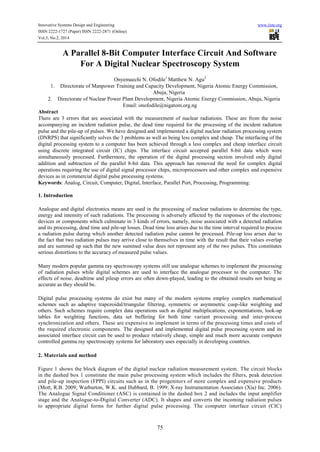
1 like•217 views


Recommended
More Related Content
What's hot
What's hot (20)
Similar to A parallel 8 bit computer interface circuit and software for a digital nuclear spectroscopy system
Similar to A parallel 8 bit computer interface circuit and software for a digital nuclear spectroscopy system (20)
More from Alexander Decker
More from Alexander Decker (20)
A parallel 8 bit computer interface circuit and software for a digital nuclear spectroscopy system
- 1. Innovative Systems Design and Engineering www.iiste.org ISSN 2222-1727 (Paper) ISSN 2222-2871 (Online) Vol.5, No.2, 2014 75 A Parallel 8-Bit Computer Interface Circuit And Software For A Digital Nuclear Spectroscopy System Onyemaechi N. Ofodile1 Matthew N. Agu2 1. Directorate of Manpower Training and Capacity Development, Nigeria Atomic Energy Commission, Abuja, Nigeria 2. Directorate of Nuclear Power Plant Development, Nigeria Atomic Energy Commission, Abuja, Nigeria Email: onofodile@nigatom.org.ng Abstract There are 3 errors that are associated with the measurement of nuclear radiations. These are from the noise accompanying an incident radiation pulse, the dead time required for the processing of the incident radiation pulse and the pile-up of pulses. We have designed and implemented a digital nuclear radiation processing system (DNRPS) that significantly solves the 3 problems as well as being less complex and cheap. The interfacing of the digital processing system to a computer has been achieved through a less complex and cheap interface circuit using discrete integrated circuit (IC) chips. The interface circuit accepted parallel 8-bit data which were simultaneously processed. Furthermore, the operation of the digital processing section involved only digital addition and subtraction of the parallel 8-bit data. This approach has removed the need for complex digital operations requiring the use of digital signal processor chips, microprocessors and other complex and expensive devices as in commercial digital pulse processing systems. Keywords: Analog, Circuit, Computer, Digital, Interface, Parallel Port, Processing, Programming. 1. Introduction Analogue and digital electronics means are used in the processing of nuclear radiations to determine the type, energy and intensity of such radiations. The processing is adversely affected by the responses of the electronic devices or components which culminate in 3 kinds of errors, namely, noise associated with a detected radiation and its processing, dead time and pile-up losses. Dead time loss arises due to the time interval required to process a radiation pulse during which another detected radiation pulse cannot be processed. Pile-up loss arises due to the fact that two radiation pulses may arrive close to themselves in time with the result that their values overlap and are summed up such that the new summed value does not represent any of the two pulses. This constitutes serious distortions to the accuracy of measured pulse values. Many modern popular gamma ray spectroscopy systems still use analogue schemes to implement the processing of radiation pulses while digital schemes are used to interface the analogue processor to the computer. The effects of noise, deadtime and pileup errors are often down-played, leading to the obtained results not being as accurate as they should be. Digital pulse processing systems do exist but many of the modern systems employ complex mathematical schemes such as adaptive trapezoidal/triangular filtering, symmetric or asymmetric cusp-like weighting and others. Such schemes require complex data operations such as digital multiplications, exponentiations, look-up tables for weighting functions, data set buffering for both time variant processing and inter-process synchronization and others. These are expensive to implement in terms of the processing times and costs of the required electronic components. The designed and implemented digital pulse processing system and its associated interface circuit can be used to produce relatively cheap, simple and much more accurate computer controlled gamma ray spectroscopy systems for laboratory uses especially in developing countries. 2. Materials and method Figure 1 shows the block diagram of the digital nuclear radiation measurement system. The circuit blocks in the dashed box 1 constitute the main pulse processing system which includes the filters, peak detection and pile-up inspection (FPPI) circuits such as in the progenitors of more complex and expensive products (Mott, R.B. 2009; Warburton, W.K. and Hubbard, B. 1999; X-ray Instrumentation Associates (Xia) Inc. 2006). The Analogue Signal Conditioner (ASC) is contained in the dashed box 2 and includes the input amplifier stage and the Analogue-to-Digital Converter (ADC). It shapes and converts the incoming radiation pulses to appropriate digital forms for further digital pulse processing. The computer interface circuit (CIC)
- 2. Innovative Systems Design and Engineering www.iiste.org ISSN 2222-1727 (Paper) ISSN 2222-2871 (Online) Vol.5, No.2, 2014 76 interfaces these two sections to the computer. The operations of the ASC, FPPI and the CIC are controlled by the computer through the DNRPS interface software. The output of the DNRPS hardware is comprised of parallel 8-bit data that require simultaneous processing. The simultaneous processing of the parallel 8-bit data results into a form that is easy for visual interpretation. To achieve this, two interface systems are needed. These are the hardware interface which links the physical pulse processing stage to the computer and the software interface that enables the hardware interface components to function with the computer. The software interface also provides a platform for further processing of the output of the digital pulse processing section and presentation in a visually interpreted form. There are various ways of interfacing a device to a computer, mostly through the various ports. The more common ports are the Universal Serial Bus (USB), the Serial and the Parallel (printer) ports. Though the Parallel port is being phased out on many recent computer systems, but it is the most commonly used port for interfacing design projects such as ours as it allows the input of up to 8 bits or the output of 8 bits at any given time. It also requires minimal external circuitry to implement many tasks. The port is composed of 4 control lines, 5 status lines and 8 data lines. It is found commonly on the back of the personal computer as a D-Type 25 Pin female connector. Besides these, it is easier to understand and implement. In view of the above, we also chose to use the parallel port. For newer computer systems without the physical parallel port, cheap USB and Serial converter cables are available to connect the CIC to such computers. In this case, the parallel port is virtual to such computers and all data are processed as if they are passed from the physical parallel port. The design of the CIC and its accompanying software is based on the parallel processing of 8-bit data which can be easily achieved using the parallel port programming approach. This approach drastically reduces the complexities of the circuits resulting to cheaper systems. In writing programs for the use of Parallel port lines, the following software registers for the various port lines of a Standard Parallel Port (SPP) can be used. The base address, usually called the Data Port or Data Register is simply used for outputting or writing data on the Parallel port's data lines (Pins 2-9). This register is normally a write only port. However, if the port is bi-directional, one can receive or read data from this address. The Status port (base address + 1) is a read only port. Any data written to this port will be ignored. The Status port is made up of 5 input lines (Pins 10,11,12,13 and 15). It is to be noted that bit 7 (Busy) is an active low input. e.g. if bit 7 shows a logic 0, then there is +5 V at pin 11. The Control port (base address + 2) is intended as a write only port but can also be used as an input port. Whenever a printer is attached to the Parallel port, four "controls" are used. These are Strobe, Auto Linefeed, Initialize and Select Printer, all of which are inverted except Initialize. The Status port is used to read the most significant nibble, MSnibble while the Control port is used to read the least significant nibble, LSnibble of the parallel 8-bit data. The Data port is used to send a parallel 8-bit data from the computer to the digital processing system either for the setting of parameters or the control of certain functions. Both the MSnibble from the Status port and the LSnibble from the Control port are combined together to form a byte using the written software. Figures 2 and 3 show the block diagram and the circuit diagram of the CIC respectively. The integrated operation of both the interface hardware (CIC) and software (DNRPS) is best explained with the circuits of Figures 2 and 3 in the following sequence. The integrated system first checks if a device is connected. Bit S7 of the Status port lines is inverted while bit S3 is used to check for connected device. By reading the Status port, if the device is connected, then the result will be &H77 (decimal 119 or binary 01110111). If no device is connected, the result will be &H7F (decimal 127 or binary 01111111) and the computer will display “No Device Found”.
- 3. Innovative Systems Design and Engineering www.iiste.org ISSN 2222-1727 (Paper) ISSN 2222-2871 (Online) Vol.5, No.2, 2014 77 After confirming a connected device, the Data port line D7 is set HIGH ie &H80 (decimal 128 or binary 10000000), causing the output of NAND gate U1A to jump HIGH, thereby arming the NAND gates U1B –U1D for further operations of loading parameters. NAND gates U1B – U1D are then programmed to go from HIGH to LOW so that values set at the D0 to D6 data lines of the Parallel Port of the computer are transferred and latched in the respective latches U2 – U4. These latched values are available to the pairs of loadable down counters DC U5 and U6, U7 and U8, U9 and U10 respectively as preset parameter values for the pulse processing sections. U5 and U6 hold the time values for the Pile-up Inspection Time (PIT), U7 and U8 hold the values for the Slow Peaking Time (SPT) while U9 and U10 hold the values for the Fast Peaking Time (FPT). With the parameter values loaded and latched, NAND gate U1A is again programmed for LOW output in order to disable any further changes to the latched output values of U2 – U4. Specifically, Data port line D7 is used for the control of NAND gate U1A. Hence, only lines D0 – D6 are available for the loading of parameter values. These Data port lines (D0 – D6) are loaded with the appropriate values, followed by a clock delay of about 200 pulses before the Control port lines are loaded with &HA, &H9, and &HF respectively, each followed by a clock delay of about 200 pulses for their corresponding parameter loading. &HA (decimal 10 or binary 00001010) means that Control port line C0 is HIGH. &H9 (decimal 9 or binary 00001001) means that Control port line C1 is HIGH. &HF (decimal 15 or binary 00001111) means that Control port line C2 is HIGH. Through the initial reset operations, the output of NAND gate U1A becomes HIGH, which makes one input each of the NAND gates U1B –U1D to become HIGH. As each Control port line C0, C1 and C2 goes HIGH and then LOW, the outputs of the NAND gates U1B – U1D will transit from HIGH to LOW and back again to HIGH, thereby latching the parameter values in their respective latches U2 – U4 and finally setting the output of NAND gate U1A LOW. Through the LOW inputs, the NAND gates U1B – U1D outputs remain HIGH irrespective of subsequent Control port values. Since Data port lines D0 – D6 (7 bits) are used for parameter values and to eliminate any accidental bit value on D7 (8th bit), any value to be loaded is first ANDed with &H7F (decimal 127 or binary 01111111). In terms of time values, the maximum peaking time is restricted to 127 multiplied by the clock pulse width. With a clock pulse width of 1.6 μS, the peaking time ranges from (127 x 1.6 μS) 1.6 μS to 203.2 μS. The pairs of loadable down counters U5 and U6, U7 and U8, U9 and U10 operate in similar manner. The counters count down from the fixed loaded values at their binary inputs provided by the U2 and U3 latches. As long as the STP, SPE and FPE connections are HIGH, the Carry-Out (CO) pins of U6, U8 and U10 ie, STE, SCO and FCO respectively remain HIGH. If STP, SPE or FPE is LOW, the respective counter starts counting down from the loaded or preset value to zero when the CO line goes LOW and then returns to HIGH on the next rising edge of the clock pulse. STP, SPE and FPE are therefore used to reset the counters to their loaded or preset values before any down counting. To control the CIC, the DNRPS software has to meet the following requirements. Recognise the presence of the digital processing device when connected to the Parallel port of the computer. In other words, it checks for the presence of device on the Parallel Port. Reset all counters, registers, flip-flops, latches etc before the commencement of operations. Load the digital processing device parameters (Pile-up Inspection Time (PIT) and the Slow channel filter Peaking Time (SPT), Fast Peak Time (FPT) and the first gain and second gain (ASC Gain) settings. Read the processed signal (data) from the output of the digital processing device, transform it into a visually interpreted form and present the final form on a computer screen.
- 4. Innovative Systems Design and Engineering www.iiste.org ISSN 2222-1727 (Paper) ISSN 2222-2871 (Online) Vol.5, No.2, 2014 78 The software can be developed using any one of the numerous programming languages such as C, C++, Delphi, Visual Basic dot Net, Matlab etc. However, the DNRPS software was developed using Visual Basic 6.0 as the interpreter and compiler. The choice of Visual Basic 6.0 is that its syntax is relatively easy to understand, being close to normal useage and logic of English language. However, there is a major limitation built into Visual Basic. It cannot directly access the hardware on a computer system. All hardware requests must pass through the Windows operating system environment especially, from Windows 95 to the recent versions XP, VISTA and Windows 7. Hence, in order to access and control the Parallel port directly, we established a link between the Parallel port hardware and the software we developed. This link can be established through the use of a Dynamic Link Library (DLL) tool known as INPOUT32.DLL. The DLL tool can be by Jan Axelson which works only on Windows 95/98/ME, or the version from LOGIX4U, which works on Windows95/98/NT/ME/2000/XP/Win7. Both can be obtained from http://www.lvr.com/parport.htm#Programming. The DLL file must be copied into the WindowsSystem folder of the computer where the interface control software is developed and/or used. 3. Results Using Figure 3, the sequence of operation of the CIC as controlled by the DNRPS software is as follow: 3.1 Device connected This is software determined. Bits 0, 1 and 3 of the Control port are inverted. Hexadecimal value &HB (decimal 11 or binary 00001011) is initially loaded on the Control port lines. The lines are then read back. As the output of the Control port lines are open collector type, the use of pull-up resistors causes zero (0) to be written to the lines. Theoritically, by reading back the lines and obtaining zero simply means that the device is connected otherwise the result will be decimal 255 or binary 11111111, meaning HIGH or open collector outputs. The sample program is: Call Out(Controlport1, &HB) “send &HB or decimal 11 or binary 1011 PortData = Inp(Controlport1) If PortData = &H0 Then “ Device is connected to Parallel port 3.2 Reset After confirming a connected device, the Control ports are set to &H0 (decimal 0 or binary 00000000), causing the output of U1A to jump HIGH, thereby arming the U1B, U1C and U1D gates for further operations of loading parameters. The sample program is: Call Out (Controlport1, &H0) “send &H0 or decimal 0 or binary “00000000 3.3 Load Parameters Loading the parameters is achieved in a sequence of Slow (PIT), followed by Fast and ASC Gain. The Data port lines are loaded with the appropriate values, followed by a clock delay of about 100 pulses before the Control port lines are loaded with &H1, &H2, &H4 and &H8 respectively, each followed by a clock delay of about 50 pulses for their corresponding parameter loading. Through the initial reset operations, the output of U1A becomes HIGH, which makes one input each of the U1B to U1D gates to become HIGH. As each Control port line C0, C1 and C2 goes HIGH and then LOW, the outputs of the U1B to U1D gates will transit from HIGH to LOW and back again to HIGH, thereby latching the parameter values in their respective Latch1 to Latch4 and finally setting the output of U1A LOW. Through the LOW inputs, the U1B to U1D outputs remain HIGH irrespective of subsequent Control port values. The sample program is: Call Out (AddressLPT1, Slow) “send Slow and Pile-up Inspection values Call Out (Controlport1, &H1) “send &H1 or decimal 1 or binary 00000001 to transfer Slow and Pile- up values to the Slow (SPT) and Pile-up Inspection (PIT) latches Call Out (AddressLPT1, Fast) “send Fast value Call Out (Controlport1, &H2) “send &H2 or decimal 2 or binary 00000010 to transfer Fast (FPT) value to the Fast latch Call Out (AddressLPT1, Gain) “send Gain and ADC Controls
- 5. Innovative Systems Design and Engineering www.iiste.org ISSN 2222-1727 (Paper) ISSN 2222-2871 (Online) Vol.5, No.2, 2014 79 Call Out (Controlport1, &H4) “send &H4 or decimal 4 or binary 00000100 to transfer Controls to the ASC Gains and ADC Start latched lines 3.4 Reading Data Data is read from the digital pulse processor through the Status and Control ports. The Status port is first read. Its value is ANDed with &HF (decimal 15 or binary 00001111) to clear the MSnibble of the Status port. Then the state of bit 3 of the Status port is checked. If it is HIGH, then data is waiting to be read from the input (C0-C3 and S4-S7) lines. To check bit 3, if the Status port value is greater than 7 but less than 16 (PortData >7 And PortData < 16), then C3 is HIGH. Thereafter, the count of occurrences of the peak value of the input line, which corresponds to a channel value, is incremented by one. The sample program is: Dim Count (1000000) PortData = (Inp(Statusport1) And &HF) If PortData >7 And PortData < 16 Then “Check if bit 3 is HIGH. If so, read data from the C0-C3 - S4- S7 lines. C3 is HIGH in the range >7 and <16 Call Out (Controlport1, &H4) PortData = (Inp(Statusport1) And &HF0) PortData = PortData Or (Inp(Controlport1) And &HF) PortData = PortData Xor &H8B “ Channel or peak value PeakCount(PortData) = PeakCount(PortData) + 1 “Increment the PeakCount by one 4. Discussion Figure 4 shows the physical realization of the CIC and the other circuit blocks of the DNRPS system while Figure 5 is the graphical user interface (GUI) displayed when the DNRPS software is run. The DNRPS software provides a general purpose visual display environment for the visual presentation of the processed information from the processing hardware. Being a general purpose GUI, no specialized statistical or analytical tools are provided. Depending on the application area, the software can be modified to include any statistical or analytical tools. The GUI has two sections: the upper section for the control and setting of parameters for the processing system and the lower section for the processing and display of captured data. In the upper section of the GUI, parameters that can be set include the Pulse Width in Shaping Amp (analogue processing) mode and Slow Peaking Time, Fast Peaking Time in Digital Filter (digital processing mode), ASC Gain and Preset Time. Once the Pulse Width/Slow Peaking Time value is selected, the Maximum Expected Count Rate is also displayed. This upper section also allows for the saving of the selected parameters, recalling of earlier saved parameter values and the configuring of the system before data collection, analyses and display can take place. The lower section of the GUI allows for the display of processed data either in graphical or numerical mode by toggling the Display Type button. Also, the default Counts Display button can be toggled for Rate display. Other facilities available in this section include opening a saved graph data file for display, saving a displayed graph data, saving a displayed graph as a picture, copying a displayed graph for pasting into other documents and printing a displayed graph. There are also facilities for zooming into a graph area for more details and selection of graph options such as colours for the grid lines, background display etc. Before data collection, processing and display are carried out, the parameters have to be set and the system configured by clicking on the Configure System button. If the hardware is not connected, there is a warning that “No Device Found”. At the end of data collection and processing, the displayed graph looks like that shown in Figure 3. There are other information available when the processed data is displayed and they include Start Processing Time, Stop Processing Time, Accumulation Time, and others such as Slow Count and Slow-Fast Peak Time Ratio when in digital filter mode. A comparison of performance with a popular analogue processing system based on the ICS-PCI computer interface card showed that the DNRPS system through the CIC provided the same kind of information as an ICS- PCI based analogue system as can be seen from Figures 5 and 6 of the GUIs respectively for the spectra of Co-
- 6. Innovative Systems Design and Engineering www.iiste.org ISSN 2222-1727 (Paper) ISSN 2222-2871 (Online) Vol.5, No.2, 2014 80 60 collected for 5 minutes. In terms of circuit complexities, the CIC circuit has just 10 cheap and readily available discrete ICs while the ICS-PCI card has complex microprocessor based circuitries. 5. Conclusion In an effort to produce a relatively cheap and less complex digital nuclear radiation processing system for gamma ray spectroscopy, we have also designed and implemented a computer interface circuit, CIC that is less complex and cheap to produce. The CIC can be used to interface any system that requires parallel processing of its 8-bit output data. Such processed 8-bit data can also be displayed in a graphical form using the implemented DNRPS software. Both the CIC and the DNRPS software offer a cheap and simple interface of a digital pulse processing system to the computer. References [1] Mott, R.B. (2009). Digital Pulse Processor Slope Correction. US Patent No US2009/0033913 A1. www.freepatentsonline.com. [2] Warburton,W.K. and Hubbard, B. (1999). Method and Apparatus for Combinatorial Logic Signal Processor in a Digitally Based High Speed X-Ray Spectrometer. US Patent No 5873054. www.freepatentsonline.com [3] X-ray Instrumentation Associates (Xia) Inc. (2006). AppNotes/DXP_Pile.pdf; microDXP Technical reference Manual, version 1.0.3. www.xia.com Configure Enable Signals 1-3 To Computer From Detector- Preamplifier INPUT AMPLIFIER STAGE Figure 1: Diagram of the Measurement System with the Component Blocks. Box 2 ASC (Analog Signal Conditioner) Box 1 FPPI (Filters, Peak detector & Pile-up inspector) CIC COMPUTER INTERFACE CIRCUIT Parallel 8-bit Data
- 7. Innovative Systems Design and Engineering www.iiste.org ISSN 2222-1727 (Paper) ISSN 2222-2871 (Online) Vol.5, No.2, 2014 81
- 8. Innovative Systems Design and Engineering www.iiste.org ISSN 2222-1727 (Paper) ISSN 2222-2871 (Online) Vol.5, No.2, 2014 82 Background Noise Counts Figure 5: DNRPS Graphical Display of Co-60 Spectra Collected for 5 Minutes Figure 4: Physical Realisation of the Computer Interface Circuit
- 9. Innovative Systems Design and Engineering www.iiste.org ISSN 2222-1727 (Paper) ISSN 2222-2871 (Online) Vol.5, No.2, 2014 83 Figure 6: ICS-PCI Display of Co-60 Spectra Collected for 5 Minutes Background Noise Counts