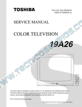
SlideShare a Scribd company logo
1 of 34
Download to read offline
SERVICE MANUAL
COLOR TELEVISION
DOCUMENT CREATED IN JAPAN, January, 2006 GREEN
19A26
FILE NO. 050-200602GR
(MFR’S VERSION A)
The above model is classified as a green product (*1), as indicated by the underlined serial number.
This Service Manual describes replacement parts for the green product. When repairing this green
product, use the part(s) described in this manual and lead-free solder (*2).
For (*1) and (*2), see the next page.
(*1) GREEN PRODUCT PROCUREMENT
The EC is actively promoting the WEEE & RoHS Directives that define standards for recycling
and reuse of Waste Electrical and Electronic Equipment and for the Restriction of the use of
certain Hazardous Substances. From July 1, 2006, the RoHS Directive will prohibit any
marketing of new products containing the restricted substances.
Increasing attention is given to issues related to the global environmental. Toshiba Corporation
recognizes environmental protection as a key management tasks, and is doing its utmost to
enhance and improve the quality and scope of its environmental activities. In line with this,
Toshiba proactively promotes Green Procurement, and seeks to purchase and use products,
parts and materials that have low environmental impacts.
Green procurement of parts is not only confined to manufacture. The same green parts used in
manufacture must also be used as replacement parts.
(*2) LEAD-FREE SOLDER
This product is manufactured using lead-free solder as a part of a movement within the consumer
products industry at large to be environmentally responsible. Lead-free solder must be used in
the servicing and repair of this product.
WARNING
This product is manufactured using lead free solder.
DO NOT USE LEAD BASED SOLDER TO REPAIR THIS PRODUCT !
The melting temperature of lead-free solder is higher than that of leaded solder by 86°F to 104°F
(30°C to 40°C). Use of a soldering iron designed for lead-based solders to repair product made
with lead-free solder may result in damage to the component and or PCB being soldered. Great
care should be made to ensure high-quality soldering when servicing this product  especially
when soldering large components, through-hole pins, and on PCBs  as the level of heat
required to melt lead-free solder is high.
A1-1
SERVICING NOTICES ON CHECKING
6. AVOID AN X-RAY1. KEEP THE NOTICES
As for the places which need special attentions,
they are indicated with the labels or seals on the
cabinet, chassis and parts. Make sure to keep the
indications and notices in the operation manual.
3. USE THE DESIGNATED PARTS
5. TAKE CARE TO DEAL WITH THE
CATHODE-RAY TUBE
Safety is secured against an X-ray by consider-
ing about the cathode-ray tube and the high
voltage peripheral circuit, etc.
Therefore, when repairing the high voltage pe-
ripheral circuit, use the designated parts and
make sure not modify the circuit.
Repairing except indicates causes rising of high
voltage, and it emits an X-ray from the cathode-
ray tube.
Please include the following informations when you order parts. (Particularly the VERSION LETTER.)
1. MODEL NUMBER and VERSION LETTER
The MODEL NUMBER can be found on the back of each product and the VERSION LETTER can be
found at the end of the SERIAL NUMBER.
2. PART NO. and DESCRIPTION
You can find it in your SERVICE MANUAL.
HOW TO ORDER PARTS
When you exchange IC and Transistor with a heat sink, apply silicon grease on the contact section of
the heat sink. Befor applying new silicon grease, remove all the old silicon grease. (Old grease may
cause damages to the IC and Transistor.)
IMPORTANT
2. AVOID AN ELECTRIC SHOCK
There is a high voltage part inside. Avoid an
electric shock while the electric current is
flowing.
The parts in this equipment have the specific
characters of incombustibility and withstand
voltage for safety. Therefore, the part which is
replaced should be used the part which has
the same character.
Especially as to the important parts for safety
which is indicated in the circuit diagram or the
table of parts as a mark, the designated
parts must be used.
4. PUT PARTS AND WIRES IN THE
ORIGINAL POSITION AFTER
ASSEMBLING OR WIRING
There are parts which use the insulation
material such as a tube or tape for safety, or
which are assembled in the condition that
these do not contact with the printed board.
The inside wiring is designed not to get closer
to the pyrogenic parts and high voltage parts.
Therefore, put these parts in the original
positions.
In the condition that an explosion-proof cathode-
ray tube is set in this equipment, safety is
secured against implosion. However, when
removing it or serving from backward, it is
dangerous to give a shock. Take enough care to
deal with it.
PERFORM A SAFETY CHECK AFTER
SERVICING
7.
Confirm that the screws, parts and wiring which
were removed in order to service are put in the
original positions, or whether there are the
portions which are deteriorated around the
serviced places serviced or not. Check the
insulation between the antenna terminal or
external metal and the AC cord plug blades.
And be sure the safety of that.
(INSULATION CHECK PROCEDURE)
1.
2.
3.
4.
Unplug the plug from the AC outlet.
Remove the antenna terminal on TV and turn
on the TV.
Insulation resistance between the cord plug
terminals and the eternal exposure metal
[Note 2] should be more than 1M ohm by
using the 500V insulation resistance meter
[Note 1].
If the insulation resistance is less than 1M
ohm, the inspection repair should be
required.
[Note 1]
If you have not the 500V insulation
resistance meter, use a Tester.
[Note 2]
External exposure metal: Antenna terminal
Headphone jack
A1-2
TABLE OF CONTENTS
A2-1
GREEN PRODUCT PROCUREMENT ........................................................................................................
LEAD-FREE SOLDER ................................................................................................................................
SERVICING NOTICES ON CHECKING ......................................................................................................
HOW TO ORDER PARTS ...........................................................................................................................
IMPORTANT ................................................................................................................................................
TABLE OF CONTENTS ..............................................................................................................................
GENERAL SPECIFICATIONS ....................................................................................................................
DISASSEMBLY INSTRUCTIONS
1.REMOVAL OF ANODE CAP ..............................................................................................................
2.REMOVAL AND INSTALLATION OF FLAT PACKAGE IC ...............................................................
SERVICE MODE LIST .................................................................................................................................
CONFIRMATION OF HOURS USED ..........................................................................................................
WHEN REPLACING EEPROM (MEMORY) IC ...........................................................................................
ELECTRICAL ADJUSTMENTS ..................................................................................................................
BLOCK DIAGRAM ......................................................................................................................................
PRINTED CIRCUIT BOARDS
MAIN/CRT...............................................................................................................................................
SCHEMATIC DIAGRAMS
MICON/CHROMA/TUNER ......................................................................................................................
TV POWER .............................................................................................................................................
DEFLECTION/CRT .................................................................................................................................
SOUND/AV .............................................................................................................................................
WAVEFORMS .............................................................................................................................................
MECHANICAL EXPLODED VIEW ..............................................................................................................
MECHANICAL REPLACEMENT PARTS LIST ..........................................................................................
ELECTRICAL REPLACEMENT PARTS LIST ............................................................................................
A1-1
A1-1
A1-2
A1-2
A1-2
A2-1
A3-1~A3-5
B1-1
B2-1, B2-2
C-1
C-1
C-1
D-1~D-4
E-1, E-2
F-1~F-4
G-1, G-2
G-3, G-4
G-5, G-6
G-7, G-8
H-1, H-2
I-1, I-2
J1-1
J2-1~ J2-3
GENERAL SPECIFICATIONS
G-1 TV CRT CRT Size / Visual Size 19 inch / 480.0mmV
System CRT Type Normal
Magnetic Field BV/BH +0.45G/0.18G
Color System NTSC
Speaker 1Speaker
Position Bottom
Size 3 Inch
Impedance 8 ohm
Sound Output MAX 1.5 W
10%(Typical) --- W
NTSC3.58+4.43 /PAL60Hz No
G-2 Tuning Broadcasting System US System M
System Tuner and System 1Tuner
Receive CH Destination USA(W/ CABLE)
2 - 69, 4A, A-5 - A-1,
CH Coverage A - I, J - W, W+1 - W+84
Intermediate Picture(FP) 45.75MHz
Frequency Sound(FS) 41.25MHz
FP-FS 4.50MHz
Preset CH No
Stereo/Dual TV Sound No
Tuner Sound Muting Yes
G-3 Power Power Source AC 120V AC 60Hz
DC
Power Consumption at AC
73 W at AC 120 V 60 Hz
Stand by (at AC) 3 W at AC 120 V 60 Hz
Per Year -- kWh/Year
Protector Power Fuse Yes
G-4 Regulation Safety UL
Radiation FCC
X-Radiation DHHS
G-5 Temperature Operation +5oC ~ +40oC
Storage -20oC ~ +60oC
G-6 Operating Humidity Less than 80% RH
A3-1
GENERAL SPECIFICATIONS
G-7 On Screen Menu Yes
Display Menu Type Character
Picture Yes
Contrast Yes
Brightness Yes
Color Yes
Tint Yes
Sharpness Yes
Audio No
Bass No
Treble No
Balance No
BBE On/Off No
Stable Sound On/Off No
CH Set Up Yes
TV/CABLE(CABLE) Yes
Auto CH Memory Yes
Add/ Delete Yes
Language Yes
V-chip Yes
Lock Yes
On Timer Yes
CH Label No
Favorite CH No
Color Stream DVD/DTV No
Control Level Yes
Volume Yes
Brightness Yes
Contrast Yes
Color Yes
Tint Yes
Sharpness Yes
Tuning No
Bass No
Treble No
Balance No
Back Light No
Stereo,Audio Output,SAP No
Video Yes
Color Stream No
Channel(TV/Cable) Yes
CH Label No
Game Timer Yes
Sleep Timer Yes
Sound Mute Yes
V-chip Rating Yes
G-8 OSD Language English French Spanish
G-9 Clock and Sleep Timer Max Time 120 Min
Timer Step 10 Min
On Timer Program(On Timer ) Yes
Wake Up Timer No
Timer Back-up (at Power Off Mode) more than -- Min Sec
A3-2
GENERAL SPECIFICATIONS
G-10 Remote Unit RC-EH
Control Glow in Dark Remocon Yes
Format Toshiba
Custom Code 40-BF h
Power Source Voltage(D.C) 3V
UM size x pcs UM-4 x 2 pcs
Total Keys 27 Keys
Keys Power Yes
1 Yes
2 Yes
3 Yes
4 Yes
5 Yes
6 Yes
7 Yes
8 Yes
9 Yes
0 Yes
100 No
CH Up Yes
CH Down Yes
Volume Up Yes
Volume Down Yes
TV/Caption/Text Yes
CH1/CH2 Yes
TV/Video(TV/AV) Yes
CH RTN/CH ENT(Quick View) Yes
Sleep Yes
RE Call(Call) Yes
Reset Yes
Menu Yes
Enter Yes
Mute Yes
Exit No
MTS(Audio Select) No
Set + Yes
Set - Yes
Multi Brand Keys CH Up(VCR) No
CH Down(VCR) No
Pause/Still No
TV/VCR(VCR) No
Code No
FF No
Rew No
Rec No
Play No
Stop No
TV No
VCR No
Cable No
A3-3
GENERAL SPECIFICATIONS
G-11 Features Auto Degauss Yes
Auto Shut Off Yes
Canal+ No
CABLE Yes
Anti-theft No
Rental No
Memory(Last CH) Yes
Memory(Last Volume) Yes
V-Chip Yes
Type USA,ORION Type
BBE No
Auto Search No
CH Allocation No
SAP No
Just Clock Function No
CH Label No
VM Circuit No
Full OSD No
Premiere No
Comb Filter No
Lines
Auto CH Memory Yes
Hotel Lock No
Closed Caption Yes
Stable Sound No
FBT Leak Test Protect Yes
CH Lock Yes
Video Lock Yes
Game Timer (Max Time:120 Min) Yes
Stable Sound No
Energy Star No
Power On Memory Yes
Favorite CH No
G-12 Accessories Owner's Manual Language English / Spanish
W/ Warranty Yes
Remote Control Unit Yes
Rod Antenna No
Poles
Terminal
Loop Antenna No
Terminal
U/V Mixer No
DC Car Cord (Center+) No
Guarantee Card No
Warning Sheet No
Circuit Diagram No
Antenna Change Plug No
Service Facility List No
Important Safety Instruction No
Dew/AHC Caution Sheet No
AC Plug Adapter No
Quick Set-up Sheet No
Battery Yes
UM size x pcs UM4 x 2
OEM Brand No
AC Cord No
AV Cord (2Pin-1Pin) No
Registration Card (NDL Card) Yes
ESP Card No
PTB Sheet No
300 ohm to 75 ohm Antenna Adapter No
A3-4
GENERAL SPECIFICATIONS
G-13 Interface Switch Front Power Yes
System Select No
Main Power SW No
Sub Power No
Channel Up/Reset Yes
Channel Down/Enter Yes
Volume Up/Set Up Yes
Volume Down/Set Down Yes
MENU=Volume Up+Volume Down Yes
Rear AC/DC No
TV/CABLE Selector No
Degauss No
Main Power SW No
Indicator Power Yes
Stand-by No
On Timer No
Terminals Front Video Input RCA
Audio Input RCA x 1
Other Terminal No
Rear Video Input(Rear1) No
Video Input(Rear2) No
Audio Input(Rear1) No
Audio Input(Rear2) No
Video Output No
Audio Output No
Euro Scart No
Color Stream No
Diversity No
Ext Speaker No
DC Jack 12V(Center +) No
VHF/UHF Antenna Input F Type
AC Outlet No
G-14 Set Size Approx. W x D x H (mm) 488 x 465 x 416
G-15 Weight Net (Approx.) 17.5kg ( 38.6 lbs)
Gross (Approx.) 20.0kg ( 44.1lbs)
G-16 Carton Master Carton No
Content ---- Sets
Material -- /--
Dimensions W x D x H(mm) -- x -- x --
Description of Origin No
Gift Box Material Double/Brown
Dimensions W x D x H(mm) 546 x 526 x 472
Description of Origin Yes
Drop Test
Natural Dropping At 1 Corner / 2
Edges / 4 Surfaces
Height (cm) 60 (ORION SPEC:46)
Container Stuffing 436 Sets/40' container
G-17 Cabinet Material Cabinet Cabinet Front PS 94V0 DECABROM
Cabinet Rear PS 94V0 DECABROM
PCB Non-Halogen Demand No
Eyelet Demand Yes
G-18 Environment Environmental standard requirement (by buyer) Green procurement of TOSHIBA
Pb-free Phase3(Ph
A3-5
B1-1
1. REMOVAL OF ANODE CAP
Read the following NOTED items before starting work.
After turning the power off there might still be a potential
voltage that is very dangerous. When removing the
Anode Cap, make sure to discharge the Anode Cap's
potential voltage.
Do not use pliers to loosen or tighten the Anode Cap
terminal, this may cause the spring to be damaged.
*
*
REMOVAL
1. Follow the steps as follows to discharge the Anode Cap.
(Refer to Fig. 1-1.)
Connect one end of an Alligator Clip to the metal part of a
flat-blade screwdriver and the other end to ground.
While holding the plastic part of the insulated Screwdriver,
touch the support of the Anode with the tip of the
Screwdriver.
A cracking noise will be heard as the voltage is discharged.
Flip up the sides of the Rubber Cap in the direction of the
arrow and remove one side of the support.
(Refer to Fig. 1-2.)
2.
DISASSEMBLY INSTRUCTIONS
GND on the CRT
Screwdriver
Alligator Clip
Support
CRT
GND on the CRT
Rubber Cap
CRT
Support
Fig. 1-1
Fig. 1-2
3. After one side is removed, pull in the opposite direction to
remove the other.
NOTE
Take care not to damage the Rubber Cap.
INSTALLATION
1. Clean the spot where the cap was located with a small
amount of alcohol. (Refer to Fig. 1-3.)
Location of Anode Cap
Fig. 1-3
NOTE
Confirm that there is no dirt, dust, etc. at the spot where
the cap was located.
2.
3.
Arrange the wire of the Anode Cap and make sure the
wire is not twisted.
Turn over the Rubber Cap. (Refer to Fig. 1-4.)
Fig. 1-4
4. Insert one end of the Anode Support into the anode button,
then the other as shown in Fig. 1-5.
5.
6.
Confirm that the Support is securely connected.
Put on the Rubber Cap without moving any parts.
CRT
Support
Fig. 1-5
B2-1
Masking Tape
(Cotton Tape)
DISASSEMBLY INSTRUCTIONS
2.
REMOVAL
IC
Put the Masking Tape (cotton tape) around the Flat
Package IC to protect other parts from any damage.
(Refer to Fig. 2-1.)
1.
Fig. 2-1
NOTE
REMOVAL AND INSTALLATION OF
FLAT PACKAGE IC
Some ICs on the PCB are affixed with glue, so be
careful not to break or damage the foil of each IC leads
or solder lands under the IC when removing it.
NOTE
Masking is carried out on all the parts located within 10
mm distance from IC leads.
Blower type IC
desoldering machine
IC
Heat the IC leads using a blower type IC desoldering
machine. (Refer to Fig. 2-2.)
2.
Fig. 2-2
NOTE
Do not add the rotating and the back and forth
directions force on the IC, until IC can move back and
forth easily after desoldering the IC leads completely.
When IC starts moving back and forth easily after
desoldering completely, pickup the corner of the IC using a
tweezers and remove the IC by moving with the IC
desoldering machine. (Refer to Fig. 2-3.)
3.
Blower type IC
desoldering
machine
IC
Fig. 2-3
Tweezers
Peel off the Masking Tape.4.
Absorb the solder left on the pattern using the Braided
Shield Wire. (Refer to Fig. 2-4.)
5.
NOTE
Do not move the Braided Shield Wire in the vertical
direction towards the IC pattern.
Braided Shield Wire
Soldering Iron
Fig. 2-4IC pattern
B2-2
DISASSEMBLY INSTRUCTIONS
Supply soldering
from upper position
to lower position
IC
Supply the solder from the upper position of IC leads
sliding to the lower position of the IC leads.
(Refer to Fig. 2-6.)
2.
Fig. 2-6
Soldering IronSolder
IC
Absorb the solder left on the lead using the Braided Shield
Wire. (Refer to Fig. 2-7.)
3.
Fig. 2-7
Soldering Iron
Braided Shield Wire
NOTE
Do not absorb the solder to excess.
IC
When bridge-soldering between terminals and/or the
soldering amount are not enough, resolder using a Thin-tip
Soldering Iron. (Refer to Fig. 2-8.)
4.
Fig. 2-8
Thin-tip Soldering Iron
NOTE
When the IC leads are bent during soldering and/or
repairing, do not repair the bending of leads. If the
bending of leads are repaired, the pattern may be
damaged. So, always be sure to replace the IC in this
case.
Finally, confirm the soldering status on four sides of the IC
using a magnifying glass.
Confirm that no abnormality is found on the soldering
position and installation position of the parts around the IC.
If some abnormality is found, correct by resoldering.
5.
Solder temporarily
Soldering Iron
INSTALLATION
Take care of the polarity of new IC and then install the new
IC fitting on the printed circuit pattern. Then solder each
lead on the diagonal positions of IC temporarily.
(Refer to Fig. 2-5.)
1.
Fig. 2-5
Solder temporarily
This unit is provided with the following SERVICE MODES so you can repair, examine and adjust easily.
To enter the Service Mode, press both set key and remote control key for more than 2 seconds.
Set Key Remocon Key Operations
VOL. (-) MIN 1
Initialization of factory data.
NOTE: Do not use this for normal servicing.
If you set factory initialization, the memories are reset such as the clock
setting, the channel setting, the POWER ON total hours.
VOL. (-) MIN 6
POWER ON total hours is displayed on the screen.
Refer to the "CONFIRMATION OF HOURS USED".
Can be checked of the INITIAL DATA of MEMORY IC.
Refer to the "WHEN REPLACING EEPROM (MEMORY) IC".
VOL. (-) MIN
Display of the Adjustment MENU on the screen.
Refer to the "ELECTRICAL ADJUSTMENT" (On-Screen Display Adjustment).
9
CONFIRMATION OF HOURS USED
POWER ON total hours can be checked on the screen. Total hours are displayed in 16 system of notation.
NOTE: If you set factory initialization, the total hours is reset to "0".
1.
2.
3.
Set the VOLUME to minimum.
Press both VOL. DOWN button on the set and Channel
button (6) on the remote control for more than 2 seconds.
After the confirmation of using hours, turn off the power.
FIG. 1
Initial setting content of MEMORY IC.
POWER ON total hours.
= (16 x 16 x 16 x thousands digit value)
+ (16 x 16 x hundreds digit value)
+ (16 x tens digit value)
+ (ones digit value)
ADDRESS DATA
INIT 00 D0
CRT ON 0010
VOL. (-) MIN 0 Releasing of V-CHIP PASSWORD.
WHEN REPLACING EEPROM (MEMORY) IC
If a service repair is undertaken where it has been required to change the MEMORY IC, the following steps should be taken to
ensure correct data settings while making reference to TABLE 1.
Table 1
1.
2.
3.
4.
5.
6.
7.
8.
9.
10.
11.
The unit will now have the correct DATA for the new MEMORY IC.
Enter DATA SET mode by setting VOLUME to minimum.
While holding down VOLUME button on front cabinet, press key (6) on remote control for more than 2 seconds.
ADDRESS and DATA should appear as FIG 1.
ADDRESS is now selected and should "blink". Using the VOL. +/- button on the remote, step through the ADDRESS until
required ADDRESS to be changed is reached.
Press ENTER to select DATA. When DATA is selected, it will "blink".
Again, step through the DATA using VOL. +/- button until required DATA value has been selected.
Pressing ENTER will take you back to ADDRESS for further selection if necessary.
Repeat steps 3 to 6 until all data has been checked.
When satisfied correct DATA has been entered, turn POWER off (return to STANDBY MODE) to finish DATA input.
After the data input, set to the initializing of shipping.
Turn POWER on.
While holding down VOLUME button on front cabinet, press key (1) on remote control for more than 2 seconds.
After the finishing of the initializing of shipping, the unit will turn off automatically.
SERVICE MODE LIST
C-1
+9+2INI +0 +1 +3 +4 +5 +6 +7
00
+8 +A
57 B3 24 69 39 00 00D0 04 EB 4E
+B +C +D +E +F
05 90 D0 00 07
ELECTRICAL ADJUSTMENTS
D-1
1.
Read and perform these adjustments when repairing the
circuits or replacing electrical parts or PCB assemblies.
CAUTION
Use an isolation transformer when performing any service
on this chassis.
Before removing the anode cap, discharge electricity
because it contains high voltage.
When removing a PCB or related component, after
unfastening or changing a wire, be sure to put the wire
back in its original position.
When you exchange IC and Transistor with a heat sink,
apply the silicon grease on the contract
section of the heat sink, Before applying new silicon
grease, remove all the old silicon grease. (Old grease
may cause damages to the IC and Transistor.)
BEFORE MAKING ELECTRICAL
ADJUSTMENTS
1. Oscilloscope
2. Digital Voltmeter
3. Pattern Generator
Prepare the following measurement tools for electrical
adjustments.
On-Screen Display Adjustment
In the condition of NO indication on the screen.
Press the VOL. DOWN button on the set and the
Channel button (9) on the remote control for more than
2 seconds to appear the adjustment mode on the
screen as shown in Fig. 1-1.
1.
Fig. 1-1
Use the Channel UP/DOWN button or Channel button
(0-9) on the remote control to select the options shown
in Fig. 1-2.
Press the MENU button on the remote control to end
the adjustments.
2.
3.
TV
00 OSD 28
2. BASIC ADJUSTMENTS
2-1: CUT OFF
1.
2.
3.
4.
5.
Place the set in AV MODE without signal.
Using the remote control, set the brightness and contrast
to normal position.
Place the set in Aging Test for more than 15 minutes.
Activate the adjustment mode display of Fig. 1-1 and
press the channel button (01) on the remote control to
select "CUT OFF".
Adjust the Screen Volume until a dim raster is obtained.
2-2: FOCUS
1.
2.
3.
Receive the monoscope pattern.
Turn the Focus Volume fully counterclockwise once.
Adjust the Focus Volume until picture is distinct.
2-3: WHITE BALANCE
NOTE: Adjust after performing CUT OFF adjustment.
Place the set in Aging Test for more than 15 minutes.
Receive the white 100% signal from the Pattern
Generator.
Using the remote control, set the brightness and
contrast to normal position.
Activate the adjustment mode display of Fig. 1-1 and
press the channel button (10) on the remote control to
select "R.BIAS".
Using the VOL. UP/DOWN button on the remote control,
adjust the R.BIAS.
Press the CH. UP/DOWN button on the remote control to
select the "R.DRIVE", "B.DRIVE", "G.BIAS" or "B.BIAS".
Using the VOL. UP/DOWN button on the remote control,
adjust the R.DRIVE, B.DRIVE, G.BIAS or B.BIAS.
Perform the above adjustments 6 and 7 until the white
color is achieved.
1.
2.
3.
4.
5.
6.
7.
8.
FUNCTION
OSD H
CUT OFF
H.VCO
H.PHASE
V.SIZE
V.SHIFT
R.DRIVE
B.DRIVE
R.BIAS
G.BIAS
B.BIAS
BRIGHT CENT
BRIGHT MAX
BRIGHT MIN
NO.
00
01
04
05
06
07
08
09
10
11
12
13
14
15
Fig. 1-2
FUNCTION
CONTRAST CENT
CONTRAST MAX
CONTRAST MIN
COLOR CENT
COLOR MAX
COLOR MIN
TINT
SHARPNESS
FM LEVEL
LEVEL
SEPARATION 1
SEPARATION 2
TEST MONO
TEST STEREO
NO.
16
17
18
19
20
21
22
23
24
25
26
27
28
29
2-4: VERTICAL SIZE
1.
2.
3.
4.
Receive the monoscope pattern from the Pattern
Generator.
Activate the adjustment mode display of Fig. 1-1 and
press the channel button (06) on the remote control to
select "V.SIZE".
Press the VOL. UP/DOWN button on the remote control
until the SHIFT quantity of the OVER SCAN on upside
and downside becomes 10 ± 1%.
Receive a broadcast and check if the picture is normal.
•
•
•
•
ELECTRICAL ADJUSTMENTS
D-2
Receive the monoscope pattern from the Pattern
Generator.
Activate the adjustment mode display of Fig. 1-1
and press the channel button (07) on the remote
control to select "V.SFT".
Press the VOL. UP/DOWN button on the remote
control until the horizontal line becomes fit to the
notch of the shadow mask.
2-7: HORIZONTAL PHASE
1.
2.
3.
Receive the monoscope pattern from the Pattern
Generator.
Activate the adjustment mode display of Fig. 1-1 and
press the channel button (05) on the remote control to
select "H.PHAS".
Press the VOL. UP/DOWN button on the remote
control until the SHIFT quantity of the OVER SCAN on
right and left becomes minimum.
Receive the monoscope pattern. (RF Input)
Activate the adjustment mode display of Fig. 1-1 and
press the channel button (13) on the remote control to
select "BRI.CENT".
Press the VOL. UP/DOWN button on the remote control
until the white 7.5% is starting to be visible.
Receive the monoscope pattern. (Audio Video Input)
Press the TV/AV button on the remote to set to the
AV mode. Then perform the above adjustment 2 and 3.
1.
2.
3.
4.
5.
2-8: BRIGHT CENTER
2-9: VERTICAL SHIFT
1.
2.
3.
2-10: OSD POSITION
1.
2.
Activate the adjustment mode display of Fig. 1-1.
Press the VOL. UP/DOWN button on the remote
control until the difference of A and B becomes
minimum. (Refer to Fig. 2-4)
BA
TV
00 OSD 28
Fig. 2-4
2-5: TINT
1.
2.
3.
4.
5.
6.
Receive the color bar pattern.(RF Input)
Connect the oscilloscope to TP023.
Activate the adjustment mode display of Fig. 1-1 and
press the channel button (22) on the remote control to
select "TINT".
Press the VOL. UP/DOWN button on the remote control
until the section "A" becomes as straight line.
(Refer to Fig. 2-1)
Receive the color bar pattern. (Audio Video Input)
Press the TV/AV button on the remote control to set to
the AV mode. Then perform the above adjustments 2~4.
2-6: COLOR CENT
1.
2.
3.
4.
5.
6.
7.
8.
9.
Receive the color bar pattern. (RF Input)
Using the remote control, set the brightness, contrast,
color, and tint to normal position.
Connect the oscilloscope to TP022.
Activate the adjustment mode display of Fig. 1-1 and
press the channel button (19) on the remote control to
select "COLOR CENT".
Adjust the VOLTS RANGE VARIABLE knob of the
oscilloscope until the range between white 100% and 0%
is set to 4 scales on the screen of the oscilloscope.
Press the VOL. UP/DOWN button on the remote control
until the red color level is adjusted to 110 ± 10% of the
white level. (Refer to Fig. 2-2)
Receive the color bar pattern. (Audio Video Input)
Press the TV/AV button on the remote control to set to
the AV mode. Then perform the above adjustments 2~5.
Press the VOL. UP/DOWN button on the remote control
until the red color level is adjusted to 100 ± 10% of the
white level. (Refer to Fig. 2-2)
Fig. 2-1
"A"
Fig. 2-2
110%
white 100%
Shadow mask
;;
;;
;;
;;
;;
;;
;;
;
Fig. 2-3
ELECTRICAL ADJUSTMENTS
D-3
2-11: CONTRAST MAX
1.
2.
3.
4.
5.
6.
7.
Receive the color bar pattern.(RF Input)
Activate the adjustment mode display of Fig. 1-1
press the channel button (17) on the remote control
to select "CONT.MAX".
Press the VOL. UP/DOWN button on the remote control
until the contrast step No. becomes "70".
Receive the color bar pattern. (Audio Video Input)
Press the TV/AV button on the remote to set to the
AV mode.
Activate the adjustment mode display of Fig. 1-1
press the channel button (17) on the remote control
to select "CONT.MAX".
Press the VOL. UP/DOWN button on the remote control
until the contrast step No. becomes "77".
2-12: Confirmation of Fixed Value (Step No.)
Please check if the fixed values of the each adjustment
items are set correctly referring below.
NO.
04
14
15
16
18
20
21
23
24
25
26
27
FUNCTION
H. VCO
BRIGHT MAX
BRIGHT MIN
CONT CENT
CONT MIN
COLOR MAX
COLOR MIN
SHARPNESS
FM LEVEL
LEVEL
SEPARTION1
SEPARTION2
STEP NO.
04
183
60
30
17
74
00
45
00
00
00
00
ELECTRICAL ADJUSTMENTS
D-4
3.
1.
2.
3.
1.
2.
3.
4.
5.
6.
7.
8.
3-2: PURITY
NOTE
Adjust after performing adjustments in section 3-1.
1.
2.
3.
4.
5.
Receive the green raster pattern from color bar
generator.
Adjust the pair of purity magnets to center the
color on the screen.
Adjust the pair of purity magnets so the color at the
ends are equally wide.
Move the deflection yoke backward (to neck side)
slowly, and stop it at the position when the whole
screen is green.
Confirm red and blue colors.
Adjust the slant of the deflection yoke while watching the
screen, then tighten the fixing screw.
DEFLECTION YOKE
DEFLECTION YOKE SCREW
MAGNET SCREW
PURITY MAGNETS
6 POLE MAGNETS
4 POLE MAGNETS
Fig. 3-1
PURITY AND CONVERGENCE
ADJUSTMENTS
NOTE
3-1: STATIC CONVERGENCE (ROUGH ADJUSTMENT)
Tighten the screw for the magnet. Refer to the adjusted
CRT for the position. (Refer to Fig. 3-1)
If the deflection yoke and magnet are in one body,
untighten the screw for the body.
Receive the green raster pattern from the color bar
generator.
Slide the deflection yoke until it touches the funnel
side of the CRT.
Adjust center of screen to green, with red and blue on the
sides, using the pair of purity magnets.
Switch the color bar generator from the green raster
pattern to the crosshatch pattern.
Combine red and blue of the 3 color crosshatch pattern
on the center of the screen by adjusting the pair of
4 pole magnets.
Combine red/blue (magenta) and green by adjusting the
pair of 6 pole magnets.
Adjust the crosshatch pattern to change to white
by repeating steps 6 and 7.
Turn the unit on and let it warm up for at least 30
minutes before performing the following adjustments.
Place the CRT surface facing east or west to reduce the
terrestrial magnetism.
Turn ON the unit and demagnetize with a Degauss Coil.
3-3: STATIC CONVERGENCE
1.
2.
3.
3-4: DYNAMIC CONVERGENCE
Adjust after performing adjustments in section 3-3.
1.
2.
Adjust the differences around the screen by moving
the deflection yoke upward/downward and right/left.
(Refer to Fig. 3-2-a)
Insert three wedges between the deflection yoke
and CRT funnel to fix the deflection yoke.
(Refer to Fig. 3-2-b)
R G B
R
G
B
Fig. 3-2-a
WEDGE WEDGE
WEDGE
WEDGE POSITION
Fig. 3-2-b
R G B
R
G
B
Receive the crosshatch pattern from the color bar
generator.
Combine red and blue of the 3 color crosshatch pattern
on the center of the screen by adjusting the pair of
4 pole magnets.
Combine red/blue (magenta) and green by adjusting the
pair of 6 pole magnets.
UPWARD/DOWNWARD SLANT RIGHT/LEFT SLANT
Adjust after performing adjustments in section 3-2.
NOTE
NOTE
ELECTRICAL ADJUSTMENTS
4. ELECTRICAL ADJUSTMENT PARTS LOCATION GUIDE (WIRING CONNECTION)
CRT PCB
MAIN PCB
D-5
CP803A
CRT
CP502
L503
S501A
S501B
CD501
ACIN
CD101A
CD101B
SPEAKER
CP802A
CP802B
TP023
TP022
R807
R803
CP401
CRT
CP806
CP801
CRTCD801
CP803B
OS
D
BLOCK DIAGRAM
78
70
69
68
67
RGB Proc.2
OSD SW
CONTRAST BRIGHTNESS
I/O
IIC
TIM
INT
PW
M
AD
MCU
CLK
VCXO
RGB OUTPUT Stage
DRIVE
CUT OFF
HV BLK
Ver.Proc.
Ver SYNC SEP
Ver.COUNT DOWN
V RAMP
Q801
RED OUT
Q802
GREEN OUT
Q803
BLUE OUT
Q402
H. DRIVE
Q401
H. OUTPUT
51
45
46
9
HV
F
S
FB401
10
1
2
3
CRT
V801
3 9 7
RGB
Heater
F 84
PUMP UP
AMP
+
-
7 52 6
V-OUT IC
IC401 STV9302B
VCC
RGB Proc.1
RGB MATRIX
COLOR CONT
ROM
RAM
38375758 16
Hor.Proc.
SYNC SEPA/Hor. VCO
Hor.COUNT DOWN
AFC-1/H COINCIDENT
AFC-2 H PHASE
1 DY
Q507
FEED BACK
T502
4
8
13
Q502
BUFFER
6
MEMORY IC
IC199
BR24L02F-WE2
POWER
VOL. DOWN
CH. DOWN
VOL. UP
CH. UP
X601
3.579545MHz
OS101
1
16
MICON/CHROMA IC
IC101 OEC7091C
Chroma Proc.
ACC/C-BPF
APC/KILLER
TINT/DEMO
IC501
PS2561AL1-1-V(W)
TU001
17
66
Q501
SWITCHING
D501~D504
RECTIFIER
Q506
SW
5662
65
SDA SCL
Q607
H.CTL
50
52
FEED BACK
SW
IC1001 AN7511
4 6
SOUND AMP
IC2 8
SPEAKER
SP1001
AC IN
F501
L503
DEGAUSS
COIL
TH501
RY501
RELAY
13
12
11
10
2620
73
2721
AT
T
34
2
J702
2
J703
76SW
OS105
D106
E-1 E-2
CMF081A
CCF073A
RISKOFFIRE-REPLACEASMARKED.SERVICEFORINFORMATIONABOUTCRITICAL
COMPONENTSSEEINSIDEBACKCOVER.
CAUTION
,
ATTENTION
INFORMATIONPOURSERVICEDESPIECE
CRITIQUE VOIR AUVERSO.,
Q602
Q606
R605
D604
D603
C621
C620_1
W803
IC1001
C1005
W036
W035
W043
D001
R602
W065
W067
C605
W058
R608
R621
R604
D606
R606
W060
C633
R616
R617
R109
Q601
Q603
W050
R615
R613
R614
R611
C628
W063
R601
X601
C601
C106
W053
W072
CP802A
CD101A
CD101B
J703 J702
TU001
R002
SW101 SW102 SW103 SW104 SW105
R505
R449
R448
R413_1
W047
W048
C427
R416
D403
R418
R424
C414
R629
IC401
W030
W010
C437
R408
D412
D509
D508
HS501
C508
TH501_1
C519
C446
C417
W006
W024
R814_1
C810
R816
R809
R811
R813_1
C808
R815
R504
TP024
TP023
TP022
TP401
R519
R509
D512
R429
FH501
FH502
F501
S501B
R806
R802
L501
C
P803B
R803
CP806
Q802_1
Q801_1
Q803_1
CP802B
S501A
C435
R518_1
R502
D515
W007
IC501
R515
R513
D528
R512
D516
R447
CP401
R507
D507
CP803A
C403
R514
C410_1
R427
D501
HS402
R520
C509
R506
R503
Q502
Q501
R542
D503
D502
CP502
D408
D405
B504
B501
R517_1
D504
R422
D510
D513
D505
D506
R407
D410
R410
AFC
H
S401
C123_1
OS101
J801
COL
+B
8V
ABL
GND
25V
12V
180V
HEATER
R423
R538
W004
R805
R807
D411
C434
RY501
Q507
D517
W041
R417
C516
W061
D514
R607
W046
D521
C622
W073
C610_1
W064
W062
C617
W816
W032
R405
C809
D404
W008
W009
W031
W807
D522
R001
R445
W054
R1001
R130
W018
W817
W029
C103
C606_1
W017
W016
C118
Q401
W005
CP601
W055
W056
W057
W020
R110
R113
R112
W069
W070
C602
W015
W071
W049
W019
R421
C440_1
R446
R403
W038
W037
W021
C448_1
C624_1
C630
D406
D409
W023
W002
R409
W013
W011
C007_1
W027
W026
W025
R119
W003
R804
C406
T401
R620
R500
Q402
C518
T502
C422
C502
C503
C505
R501
C515
C514_1
C517_1
C418
C
819_1
C443
W051
W040
W045
W834
R603
C623
W066
D602
W068
W033
R704_1
W812
C447
W001
R406
W059
R510
R522
D525
C511
W039
L001
W044
W052
W042
W028
R508
S802Y
S802X
FB401
W080
W034
CD501
W833
W837
W811
W809
W836
W827
W819
W832
W808
Q503 C507
R523
R527
R525
R537
R415
CP503
C526
R121
Q105
CP801_1
L801
D106_1
D611
C521_1
PRINTED CIRCUIT BOARDS
MAIN/CRT (INSERTED PARTS)
SOLDER SIDE
F-1 F-2
CMF081A
CCF073A
1
25
41
64
C1004
R1003
R004R003
R610
C101
C609
R618
C112C629
C626
C627
C604
C104
C102
IC
101
R702
R703
R128
R126
R101
R143_1
R1008
R420
R419
C501
R532
R531
C603
R104
C108_1
C107
C105
R102
R103
R125
R609
R115
C001
R1005
R1004
R127
R116_1
R627
R124
R106_1
R105_1
R107
R108
R129
IC199
C1001
Q505
Q607
Q506
C510
R516_1
C612
C614
R701
C616
C615
R134_1
C513_1
C004_1
PRINTED CIRCUIT BOARDS
MAIN/CRT (CHIP MOUNTED PARTS)
SOLDER SIDE
F-3 F-4
A B C D E F G H
A B C D E F G H
2
1
3
4
5
6
7
8
2
1
3
4
5
6
7
8
Q105
KRA102MAT
SWITCHING
D106_1
SLR-342VCT32
POWERON/ONTIMER
WAS RECEIVED IN GOOD CONDITION AND PICTURE IS NORMAL.
WITH THE DIGITAL TESTER WHEN THE COLOR BROADCAST
NOTE:THE DC VOLTAGE AT EACH PART WAS MEASURED
C604
0.022F
C007_1
0.022F
C112
100PCH
C624_1
163VMKT
C626
0.01B
C108_1
0.001B
C614
1 B C612
1 B
C104
0.01B
C102
0.01 B
C627
0.01B
C001
0.01 F
C004_1
0.022B
C629
0.01 B
C620_1
0.01 B
C105470PB
C107220PB
C609
0.01 BC602
0.1F
C603
22PCH
C101
0.01 B
C616
1 B
C615
1 B
C633
1050VYK
C605
150VKAC606_1
1006.3VYK
C601
150VKA
C123_1
1050VYK
C106
150VKA
C103
4706.3VYK
C617
10010V YK
C628
150VKA
C623
2.250V KA
C622
150V KA
C630
47010V YK
C621
4716V YK
C118
4706.3V YK
C610_1
4716V YK
R617
47K1/4W
R110
10K 1/4W
R109
10K 1/4W
R627
10K
R107
100
R108
100
R106_1
4.7K
R130
10K 1/4W
R004
100
R003
100
R105_1
4.7K
R121
2701/4W
R002
15K 1/2W
R001
15K 1/2W
R610
12K
R611
10K1/4W
R601
8.2K1/4W
R620
1K1/2W
R618
22K
R143_1
10
R115 22K
R116_1 2.2K
R6131001/4W
R6141001/4W
R102
1K
R602
1001/4W
R603
120 1/2W
R605
220 1/2W
R606
22K 1/4W
R607
100 1/4W
R6151001/4W
R126
2.7K
R101
560
R621
220 1/4W
R608
1K 1/4W
R604
100 1/4W
R104
1M
R128
560
R127
1K
R609
120K
R124
10K
R125
47K
R129
47K
R119
22K 1/4W
R1031K
R112 2.2K 1/4W
R113 2.2K 1/4W
R616
1K1/4W
R134_1
4.7K
OF PRINTING AND SUBJECT TO CHANGE WITHOUT NOTICE
NOTE:THIS SCHEMATIC DIAGRAM IS THE LATEST AT THE TIME
DANS LA NOMENCLATURE DES PIECES
N’UTILISER QUE CELLS DECRITES
DANGEREUSES AN POINT DE VUE SECURITE
:LES PIECES REPAREES PAR UN ETANTATTENTION:SINCE THESE PARTS MARKED BYCAUTION
DESCRIBED IN PARTS LIST ONLY
CRITICAL FOR SAFETY,USE ONES
ARE
W833
W808
W809
W816
IC199
BR24L02F-WE2
MEMORYIC
1 2 3 4
5678
D604
MTZJ8.2B
D611
MTZJ12B
D001
MTZJ33B
D602
MTZJ9.1B
D603
1SS133
D60611E1-EIC
Q601
KTC3203_Y
5V REG
Q602
KTC3203_Y
5V REG
Q603
KTC3203_Y
5V REG
Q606
KTC3203_Y
8V REG
Q607
2SC2412K
H.CTL
R629
22 3W
CAUTION: DIGITAL TRANSISTOR
IC101
OEC7091C
MICON/CHROMA IC
1 10 11 12 13 14 15 16 17 18 192 20 21 22 23 24
2526272829
3
30313233343536373839
4
40
414243444546474849
5
50515253545556575859
6
6061626364
6566676869
7
70717273747576777879
8
80
9
SW104
EVQ21505R
VOLDOWN
SW103
EVQ21505R
VOLUP
SW102
EVQ21505R
CHDOWN
SW101
EVQ21505R
CHUP
SW105
EVQ21505R
POWER
X601
100BT3R537
3.579545MHz
CP601
A2001WR2-6P
1
2
3
4
5
6
L001
3.3uH 0305
TU001
115-V-KA35ARH
1
10
11
12
13
14
15
16
17
18
19
2
20
21
3
4
5
6
7
8
9
S802Y
S802X
GND
B+
Vout
OS101
ROM-V3138SY
1
2
3
P.CON+5V
P.CON+5V
H_OUT
H_CTL
ABCL
CLAMP
H_CTL
G.OUT
R.OUT
H_SYNC
STANDBY_H
B.OUT
DEGAUSS_H
P.CON+B
V_OUT
GND
V_FEEDBACK
AT+5V
ABCL
H_OUT
X-RAY
SDA
R.OUT
G.OUTSCL
B.OUT
H_SYNC
AFT
UNREG+12V
STANDBY_H
KEY1 V_OUT
POWER_FAIL
UNREG+12VKEY2 V_FEEDBACK
X-RAY
GNDPOWER_ON
P.CON+5V
REMOCON
DEGAUSS_H
AT+5V
AUDIO_OUT
AUDIO_MUTE
X-RAY
AUDIO_MUTEP.CON+5V
IIC_OFF
VIDEO_INTUNER+5V
AUDIO_IN
ON_TIMER
AUDIO_OUT
P.CON+5V
GND
POWER_FAIL AUDIO_IN
VIDEO_IN
TUNER+5V
AT+5V
TU_VIDEO
TU_AUDIO
ON_TIMER
SCL
KEY1
KEY2
REMOCON
AT+5V
POWER_ON
SDA
AFT
IIC_OFF
TU_AUDIO SDA
SCL
P.CON+B
TU_VIDEO
PCB070
4.8
4.8 TEST POINT
SCL
SDA
IIC_OFF
GND
NC
NC
G-2G-1
CMF081
4.9
0
4.9
NC
0
3
NC
NC
NC
NC
NC
(MAIN PCB)
MICON/CHROMA/TUNER SCHEMATIC DIAGRAM
8.8
5.5
4.9
4.9
7.2
5.5
5.5
7.2
4.9
8.5
6 MCU VCC
7 TEST0
8 FILT
9 HLT
5 VSS
1 CNVSS
2 XIN
3 XOUT
4 TEST1
11 CVIN
10 VHOLD
12 RESET IN
13 MCU RESET OUT
14 Y SW OUT
15 V/C GND
16 3.58 XTAL
17 C-APC
18 MCU5.7V REG OUT
19 NC
20 CVBS IN3
21 AUDIO IN3
22 V/C VCC
23 MCU TEST
24 CVBS IN2
25 AUDIO IN2
26 CVBS IN1
27 AUDIO IN1
28 5.7V REG OUT
29 C(Y/C) IN
33 MONITOR OUT
32 FSC OUT
31 VREG VCC
30 Y(Y/C) IN
34 AUDIO ATT OUT
37 V RAMP F/B
38 V RAMP OUT
39 V RAMP CAP
40 8.7V REG OUT
Ver SYNC SEP
Ver.COUNT DOWN
V RAMP
Ver.Proc.
Hor.Proc.
SYNC SEPA/Hor.VCO
Hor.COUNT DOWN
AFC-1/H COINCIDENT
AFC-2 H PHASE
PGB OUTPUT Stage
DRIVE
CUT-OFF
HV BLK
IIC BUS
DECODER
OSD
ROM
RAM
CCD
CPU core
VCO
XO
COLOR CONT
RGB MATRIX
RGB Proc.1
RGB Proc.2
OSD SW
CONTRAST
BRIGHTNESS
MCU RESET
Power Manage.
MCU
CLK Y MUTE
BLACK STRETCH
Vldeo Proc.
C-TRAP/YDELAY
SHARPNESS
Chroma Proc.
ACC/C-BPF
APC/KILLER
TINT/DEMO
ATT
VCXO
LPF
6bB AMP
MCU GND
IIC
TIM
AD
PWM
INT
I/O
CLK CONT
P-ON CONT
SDA/SCL
NC
NC
4.8
NC
NC
NC
NC
NC
35 AUDIO ATT FILTER
41 NC
42 HVCO F/B
43 AFC FILTER
44 DEF GND
45 FBP IN
46 H OUT
47 DEF VCC
48 NC
49 HI VCC
50 R OUT
51 G OUT
52 B OUT
53 ACL
54 NC
55 PROTECT
56 SDA
57 H_CTL
58 SCL
62 DEGAUSS_H
63 STANDBY_H
64 VOLUME
66 AFT
67 KEY1
68 KEY2
71 AV2
72 AV1
73 AUDIO_MUTE
77 SYNC
78 POWER FAIL
80 EXT_MUTE
76 ON_TIMER
60 NC
61 NC
79 NC
75 IIC_OFF
65 NC
59 NC
NC
NC
NC
NC
70 REMOCON
69 POWER_ON
74 X-RAY
36 TEST 3
NC
NC
NC
NC
NC
5.6
NC NC
0 0 5.0 5.0 0 4.9 0 1.2 2.0 0.8 3.4 4.9 5.0 3.4 0 3.4 2.9 5.6
NC
2.82.90 5.0 0 2.0
2.2
2.0
8.8
4.6
2.3
4.5
0
2.6
5.7
2.3
3.3
4.0
4.6
3.1
8.8
2.0
03.73.404.68.008.03.53.23.22.34.604.90.34.90000
2.4
4.9
4.9
4.9
4.9
0
4.9
4.9
2.9
4.9
0
0
4.9
0
0
4.9
4.9
7.911.3
2
5 6 7
4
1
4.9 5
FROM/TO DEFLECTION/CRT
FROM/TO TV POWER
FROM/TO SOUND/AV
VSS
E2
E1
E0VCC
MODE
SDA
SCL
4.9 4.9 4.9
0 0 0 0
0
A B C D E F G H
A B C D E F G H
2
1
3
4
5
6
7
8
2
1
3
4
5
6
7
8
CP503
003P-2100
1
C515
100016VYK
C516
1050VYK
C519
100016VYK
C521_1
220200VYXF
CP502
A1561WV2-2P
1
2
HS501
763WSAA029
R518_1
5.6K+-1%
R514
0.22 1W
S501A
S501B
IS NON POLAR ONE.
THE ALUMI ELECTROLYTIC CAPACITOR MARKED NP
THE RESISTOR MARKED F IS FUSE RESISTOR.NOTE:
Q505
2SA1037AK
P.FAIL
Q503
2SA1624
PROTECT DRIVE
R501
3.3 5W C
L501
ELF15N010AP
COIL,LINE FILTER
1 2
3 4
21
L503
8R200031
DEGAUSS COIL
FH502
EYF-52BCY
FH501
EYF-52BCY
F501
4A125V
4A125V
IC501
PS2561AL1-1-V(W)
FEED BACK
12
34
B501
W5RH3.5X5X1.0
B504
W5RH3.5X5X1.0
TH501_1
B59203-S1060-B14
4A 125V
4A 125V
TYPE 4A 125V (F501).
D’INCEIE N’UTILISER QUE DES FUSIBLE DE MEME
:POUR UNE PROTECTION CONTINUE LES RISQUESATTENTION
FUSE.
REPLACE ONLY WITH THE SAME TYPE 4A 125V (F501)
CAUTION:FOR CONTINUED PROTECTION AGAINST FIRE HAZARD,
S
D
G
Q501
2SK3563(ORION_Q)
POWERAMP
BLACK
WHITE
BLADE
WIDE
CD501
09414909
AC120V_60Hz
RY501
ALKS321
1 2
3
4
T502
8129109S
11
12
13
14
15
16
17
18
2
3
4
5
6
7
8
WAS RECEIVED IN GOOD CONDITION AND PICTURE IS NORMAL.
WITH THE DIGITAL TESTER WHEN THE COLOR BROADCAST
NOTE:THE DC VOLTAGE AT EACH PART WAS MEASURED
C509
0.047 M
C501
0.0082B
C510
0.1 B
C514_1
820P2KVRR
C518
470P500V B
C517_1
820P2KV RR
C508
0.0047250V KX
C502
0.001500VB
C513_1
0.001B
C503
0.001500VB
C505
0.33275VECQUL
C526
220200VYK
C511
150V KA
C507
10100VMHE
R506
1K1/4W
R516_1
10K
R515
120K1/2W
R509
2201/4W
R520
12K1/4W
R503
1001/4W
R508
220 1/2W
R502
1K1/4W
R537
100K 1/4W
R505
1K 1/4W
R513
2.2K1/4W
R522
1.2M1/2W
R510
1.2M1/2W
R523
47K 1/4W
R527
5.6K 1/4W
R512
1K 1/4W
R504
100 1/4W
R500
2.7M1/2W
+-10%
R538
1.5M1/2W
R532
10K
R531
10K
R519
1K 1/4W
R507
1001/4W
OF PRINTING AND SUBJECT TO CHANGE WITHOUT NOTICE
NOTE:THIS SCHEMATIC DIAGRAM IS THE LATEST AT THE TIME
DANS LA NOMENCLATURE DES PIECES
N’UTILISER QUE CELLS DECRITES
DANGEREUSES AN POINT DE VUE SECURITE
:LES PIECES REPAREES PAR UN ETANTATTENTION:SINCE THESE PARTS MARKED BYCAUTION
DESCRIBED IN PARTS LIST ONLY
CRITICAL FOR SAFETY,USE ONES
ARE
W827
W819
W836
W834
W832
D506
MTZJ18B
D525
MTZJ3.6B
D507
MTZJ2.2B
D521
MTZJ10B-EIC
D528
MTZJ5.6B
D509
MTZJ18B
D514
1SS133
D508
1SS133
D512
1SS133
D522
1SS133
D505
21DQ09N
D501
1N4005-EIC
D516
1N4937-PAN
D513
21DQ09N
D517
1SS133
D515
1SS133
D504
1N4005-EIC
D510
RU2AM-EIC
D502
1N4005-EIC
D503
1N4005-EIC
Q502
KTC3198
BUFFER
Q507
KTC3198
FEED BACK
SWITCHING
Q506
2SC2412K
SW
R542
0.471W
R525
1.5 2W
R517_1
2.7 1W
GND
SOUND+B
SOUND_GND
+B
UNREG+12V
P.CON+B
GND
POWER_FAIL
DEGAUSS_H
X-RAY
UNREG+12V
AT+5V
GND
0
2.1
5.3
G-4G-3
PCB010
CMF081
0.1
0
4.8
144.0
0.1
4.8
4.9
0
4.8
(MAIN PCB)
TV POWER SCHEMATIC DIAGRAM
9.50.1
10.511.5
NC
NC
0
0
1.7
NC 0
132.3
11.3
NC
144.0
10.3
6.6
10.3
10.0
FROM/TO MICON/CHROMA/TUNER
TO SOUND/AV
9.5
5.5
6.0
FROM/TO DEFLECTION/CRT
135.0 0
135.0
A B C D E F G H
A B C D E F G H
2
1
3
4
5
6
7
8
2
1
3
4
5
6
7
8
L801
100uH
TP022 TP024 TP023
TP401
CP401
A1561WV2-A5P
1
2
3
4
5
IC401 STV9302BV-OUT IC
1 2 3 4 5 6 7
T401
STP-03Q24
1
2
3 4
6
B
G
R
11
6
8
10
9
175
V801
A48AKH13X04
F
J801
ISMP01S
1
3
4
5
6
7
8
9
CD801
CH823004
Q401
2SC5885
H.OUTPUT
VIDEO
8
E8
E25
E12
GND
TER
HEA
AFC
B+
GND
ABL
GND
COL
HV
F
S
FB401
FQI20B103_M
1
10
11
2
3
4
5
6
7
8
9
CP803B B2013H02-4P
1
2
3
4
CP803A B2013H02-4P
1
2
3
4
CP802A
B2013H02-5P
1
2
3
4
5
CP802B
B2013H02-5P
1
2
3
4
5
C427
1050VYK
C417
2250VYK
CP801_1
A2361WV2-2P
1
2
HS402
763WSA0043
HS401
763WSAA029
R408
10K+-1%
R409
56K +-1%
R429
3.9 1W
CP806
IS NON POLAR ONE.
THE ALUMI ELECTROLYTIC CAPACITOR MARKED NP
THE RESISTOR MARKED F IS FUSE RESISTOR.NOTE:
WAS RECEIVED IN GOOD CONDITION AND PICTURE IS NORMAL.
WITH THE DIGITAL TESTER WHEN THE COLOR BROADCAST
NOTE:THE DC VOLTAGE AT EACH PART WAS MEASURED
C443
0.00721.25KVPHE
C410_1
0.001CH
C437
0.33250VPMS
C819_1
0.0012KVB
C440_1
0.0012500VB
C809
390PB
C808
390PB
C810
390PB
C422
0.15100VMKT
C406
220P500V B
C447
150VYK
C448_1
22250VYK
C446
2250VYK
C414
10035V
YK
C418
47025VYK
C403
47035VYK
C435
0.1100V
MHE
C434
22100VYK
R420
4.7K
R802
2.7K1/4W
R415
1.8K 1/2W
R813_1
3301/4W
R814_1
4.7K1/4W
R413_1
2.2K1/2W
R815
3301/4W
R421
220K1/4W
R445
150K 1/4W
R806
2.7K1/4W
R410
3301/2W
R816
3301/4W
R407
3.9
1/2W
R422
3.91/2W
R419
680
R417
8.2K1/4W
R418
22K 1/4W
R446
4701/2W
R423
100 1/4W
R424
6.8K 1/4W
R804
2.7K1/4W
R811
4.7K1/4W
R809
4.7K1/4W
R403
10K 1/4W
R448
680 1/2W
R449
680 1/2W
R427
1001/4W
R405
1K1/4W
R416
11/2W
OF PRINTING AND SUBJECT TO CHANGE WITHOUT NOTICE
NOTE:THIS SCHEMATIC DIAGRAM IS THE LATEST AT THE TIME
DANS LA NOMENCLATURE DES PIECES
N’UTILISER QUE CELLS DECRITES
DANGEREUSES AN POINT DE VUE SECURITE
:LES PIECES REPAREES PAR UN ETANTATTENTION
:SINCE THESE PARTS MARKED BYCAUTION
DESCRIBED IN PARTS LIST ONLY
CRITICAL FOR SAFETY,USE ONES
ARE
W837
W817
D412
MTZJ5.1B
D404
MTZJ6.2B
D403
1N4002-PAN
D410
AU02A-EIC
D405
1N4937-PAN
D408
1N4002-PAN
D409
11E1-EIC
D406
1N4002-PAN
D411
AU02A-EIC
Q803_1
KTC4217
BLUE OUT
Q802_1
KTC4217
GREEN OUT
Q801_1
KTC4217
RED OUT
Q402
2SC1627_Y
H.DRIVE
R803
12K2W
R805
12K2W
R807
12K2W
R447
150 2W
R406
11W
GND GND
CLAMP
CLAMP CLAMP
G.OUT
G.OUT G.OUT
R.OUT
R.OUT R.OUT
B.OUT
B.OUT B.OUT
HEATER HEATER
GND GND
180V 180V
X-RAY
P.CON+B
GND
V_FEEDBACK
V_OUT
ABCL
H_OUT
H_SYNC
GND
+B
P.CON+B
UNREG+12V
PCB070
(MAIN PCB)DEFLECTION/CRT SCHEMATIC DIAGRAM
CCF073
G-6G-5
CMF081
9
126.0
NC
NC
NC
3.2
2.7
120.5
2.7
3.23.2
128.0
SCREEN
FOCUS
FOCUS
SCREEN
2
1
130.0
0
0
0
27.0
0.3
3.5 2.0 12.0 25.0 3.5
0
025.0
4.3
TO DY
NC
00
0
101.6
6.4 99.6
96.4
2.7
AMP
THERMAL
PROTECTION
PUMP
UP NC NC
GND GND
CLAMP CLAMP
G.OUT G.OUT
R.OUT R.OUT
B.OUT B.OUT
HEATER
GND
NC
180V
PCB110
FROM/TO TV POWER
FROM/TO MICON//CHROMA/TUNER
FROM MICON/CHROMA/TUNER
HEATER
GND
NC
180V
14 15 16
13
12
8
10
11
130.0
132.5
132.5
48.0
7.0
0
25.0
0
A B C D E F G H
A B C D E F G H
2
1
3
4
5
6
7
8
2
1
3
4
5
6
7
8
SPEAKER
SP1001
S08F21A
8 OHM
H
E
J703
AV1-09AD-4
RCA JACK WHITE
1
2
H
E
J702
AV1-09AD-3
RCA JACK YELLOW
1
2
TM101
RC-EH050(CT-859) BT002
GR03X-SP2
UM-4
BT001
GR03X-SP2
UM-4
CD101B
CH013208
CD101A
CH013209
WAS RECEIVED IN GOOD CONDITION AND PICTURE IS NORMAL.
WITH THE DIGITAL TESTER WHEN THE COLOR BROADCAST
NOTE:THE DC VOLTAGE AT EACH PART WAS MEASURED
C1001
0.1 B
C1004
0.0015B
C1005
1050VYK
R1003
68K
R1005
270K
R1004
100K
R1001
47K 1/4W
R1008
39K
R704_1
10 1/4W
R703
820
R701
68
R702
47K
OF PRINTING AND SUBJECT TO CHANGE WITHOUT NOTICE
NOTE:THIS SCHEMATIC DIAGRAM IS THE LATEST AT THE TIME
DANS LA NOMENCLATURE DES PIECES
N’UTILISER QUE CELLS DECRITES
DANGEREUSES AN POINT DE VUE SECURITE
:LES PIECES REPAREES PAR UN ETANTATTENTION:SINCE THESE PARTS MARKED BYCAUTION
DESCRIBED IN PARTS LIST ONLY
CRITICAL FOR SAFETY,USE ONES
ARE
W807
W812
W803
W811
IC1001
AN7511
SOUNDAMPIC
1234
5 6 7 8
AUDIO_IN
VIDEO_IN
GND
SOUND_GND
SOUND+B
GND
AUDIO_MUTE
P.CON+5V
GND
AUDIO_OUT
PCB070
G-8G-7
CMF081
-+
0
08.2 3.5 3.4
3.95.1 0.3
11
22
17
18
FROM TV POWER
FROM MICON/CHROMA/TUNER
VIDEO 2
AUDIO 2
(FRONT)
V_IN
A_IN
TO MICON/CHROMA/TUNER
19
20
ACCESSORY
SOUND/AV SCHEMATIC DIAGRAM
(MAIN PCB)
WAVEFORMS
H-1
6 1V 20µs/div
NOTE: The following waveforms were measured at the point of the corresponding
balloon number in the schematic diagram.
MICON/CHROMA/TUNER
1 0.5V 2ms/div 200V 20µs/div11
1V 20µs/div72 20V 20µs/div
DEFLECTION/CRT
10V 5ms/div12
3 200mV 20µs/div 8 0.5V 5ms/div 10V 5ms/div13
0.5V 5ms/div4 9 20V 20µs/div 50V 20µs/div14
10 2V 20µs/div5 1V 20µs/div 15 50V 20µs/div
WAVEFORMS
H-2
16 50V 20µs/div
NOTE: The following waveforms were measured at the point of the corresponding
balloon number in the schematic diagram.
SOUND/AV
0.5V 1ms/div17
1V 1ms/div18
200mV 500µs/div19
20 500mV 20µs/div
MECHANICAL EXPLODED VIEW
I-1
PCB070
(MAIN PCB ASS'Y)
203
201
107
203
106
102
205
205
205
105
205
103
101
101A
101C
101B
101D
202
108
206
206
109
109
204
204
204
204
104
PCB110
(CRT PCB ASS'Y)
109
109
MECHANICAL EXPLODED VIEW
(PACKING DIAGRAM)
I-2
117
115
118
116
110, 111, 114,
TM101
116
119
113
112
MECHANICAL REPLACEMENT PARTS LIST
Location No. TSB P/N Reference No. Description
101 72795617 7A701A420A FRONT CABI ASS'Y
101A 72795585 701WPJD025 CABINET FRONT
101B 72795615 713WPAA046 GLASS LED
101C 72795613 713WPAA050 GUIDE REMOCON
101D 72795588 735WPBA980 BUTTON FRAME
102 72783473 A3X301Q740 CABINET,BACK ASSY
103 72783474 726000A032 SHEET CRT SERVICEMAN
104 72795687 741WUA0021 SPRING EARTH
105 72783475 722549A566 SHEET RATING
106 72795622 800WQ0A110 FELT SHEET
107 72794734 899HV3T000 HOLDER ANODE WIRE
108 72795611 735WPAA938 HOLDER SPEAKER
109 72783235 800WR0A010 SHEET CRT SUPPORT (D)
110 72781569 J3N51617A REGISTRATION CARD
111 72783476 J3X00121A INSTRUCTION BOOK(E/S)
112 72795703 791WHAA134 LIGHTRON SHEET
113 72783477 723000D249 SHEET BARCODE
114 72783478 JB5ND200 POLYBAG INSTRUCTION(RED CAUTION)
115 72795621 791WHAA126 FILM BAG
116 72783479 792WHAA204 PACKAGE TOP
117 72798723 792WHAA055 PACKAGE BOTTOM
118 72783480 793WCDD067 GIFT BOX
119 72783481 A3X001V975 INSTRUCTION BOOK KIT
201 72798786 810763080U SCREW TAP TITE(S) BRAZIER 3*8 CH
202 72798791 8110630A0U SCREW TAP TITE(P) BRAZIER 3*10 CH
203 72781255 8109I3080U SCREW TAP TITE(B) WH7 3*8 CH
204 72781294 8160H50B8U SCREW TAP TITE(P) W5*28CH FLAT
205 72781279 8117540A6U SCREW TAP TITE(B0) TRUSS 4*16 CH
206 72781272 8110630A2U SCREW TAP TITE(P) BRAZIER 3*12 CH
J1-1
ELECTRICAL REPLACEMENT PARTS LIST
Location No. TSB P/N Reference No. Description
RESISTORS
R406 72781668 R3K181010J R,METAL 1 OHM 1W
! R407 72797796 R002T23R9J RC 3.9 OHM 1/2W
! R408 72796016 R4X5T6103F R,METAL 10K OHM 1/6W
! R409 72797966 R4X5T6563F R,METAL 56K OHM 1/6W
! R429 72795521 R638813R9J R,FUSE 3.9 OHM 1W
! R447 72781689 R3K58A151J R,METAL OXIDE 150 OHM 2W
! R500 72794631 R0G3K2275K RC 2.7M OHM 1/2W
! R501 72795522 R5X2CD3R3J R,CEMENT 3.3 OHM 5W
! R514 72794633 R63881R22J R,FUSE 0.22 OHM 1W
! R517 72797849 R3X1812R7J R,METAL OXIDE 2.7 OHM 1W
! R518 72795514 R4X5T6562F R,METAL 5.6K OHM 1/6W
! R525 72797898 R3X28A010J R,METAL OXIDE 1 OHM 2W
! R538 72795500 R002T2155J RC 1.5M OHM 1/2W
! R542 72781684 R3K581R47J R,METAL OXIDE 0.47 OHM 1W
! R629 72781701 R3K58B220J R,METAL OXIDE 22 OHM 3W
! R803 72781688 R3K58A123J R,METAL OXIDE 12K OHM 2W
! R805 72781688 R3K58A123J R,METAL OXIDE 12K OHM 2W
! R807 72781688 R3K58A123J R,METAL OXIDE 12K OHM 2W
CAPACITORS
! C418 72795628 E02LT3471M CE 470 UF 25V
! C434 72794396 E02LU8220M CE 22 UF 100V
C437 72795565 P4J7F3334J CMPP 0.33 UF 250V PMS
! C443 72783482 P4G8FJ722H CMPP 0.0072UF 1.25KV PHE
! C446 72794379 E02LU5220M CE 22 UF 50V
! C447 72794416 E02LU5010M CE 1 UF 50V
C448 72796351 E02LTD220M CE 22 UF 250V
! C503 72795629 C0JTB0513K CC 0.001 UF 500V B
! C505 72794401 P2122B334M CMP 0.33 UF 275V ECQUL
! C508 72795579 CD39E0MQ3M CC 0.0047UF 250V
! C514 72795580 C0PLRR7W2K CC 820 PF 2KV RR
! C515 72794425 E02LT2102M CE 1000 UF 16V
! C517 72795580 C0PLRR7W2K CC 820 PF 2KV RR
! C518 72796329 C0JTB05Q2K CC 470 PF 500V B
! C519 72794425 E02LT2102M CE 1000 UF 16V
! C521 72794411 E62NFC221M CE 220 UF 200V
! C526 72797379 E02LFC221M CE 220 UF 200V
C819 72795578 C0JBB0713K CC 0.001 UF 2KV B
DIODES
D001 72794465 D97U03301B DIODE,ZENER MTZJ33B T-77
D106 72795529 0021721150 LED SLR-342VCT32
D403 72783209 D2MXN40020 DIODE,FAST RECOVERY 1N4002-PAN
D404 72794490 D97U06R21B DIODE,ZENER MTZJ6.2B T-77
! D405 72795543 D2MXN49370 DIODE,FAST RECOVERY 1N4937-PAN
D406 72783209 D2MXN40020 DIODE,FAST RECOVERY 1N4002-PAN
D408 72783209 D2MXN40020 DIODE,FAST RECOVERY 1N4002-PAN
D409 72794488 D2WT011E10 DIODE,SILICON 11E1-EIC
! D410 72794472 D2WTAU02A0 DIODE,SILICON AU02A-EIC
! D411 72794472 D2WTAU02A0 DIODE,SILICON AU02A-EIC
! D412 72794469 D97U05R11B DIODE,ZENER MTZJ5.1B T-77
! D501 72795626 D2WXN40050 DIODE,SILICON 1N4005-EIC
! D502 72795626 D2WXN40050 DIODE,SILICON 1N4005-EIC
! D503 72795626 D2WXN40050 DIODE,SILICON 1N4005-EIC
! D504 72795626 D2WXN40050 DIODE,SILICON 1N4005-EIC
! D505 72794480 D28T21DQN9 DIODE,SCHOTTKY 21DQ09N-TA2B1
D506 72795541 D97U01801B DIODE,ZENER MTZJ18B T-77
D507 72794468 D97U02R21B DIODE,ZENER MTZJ2.2B T-77
D508 72794491 D1VT001330 DIODE,SILICON 1SS133T-77
! D509 72795541 D97U01801B DIODE,ZENER MTZJ18B T-77
! D510 72795545 D2WXRU2AM0 DIODE,SILICON RU2AM-EIC
! D512 72794491 D1VT001330 DIODE,SILICON 1SS133T-77
! D513 72794480 D28T21DQN9 DIODE,SCHOTTKY 21DQ09N-TA2B1
D514 72794491 D1VT001330 DIODE,SILICON 1SS133T-77
D515 72794491 D1VT001330 DIODE,SILICON 1SS133T-77
! D516 72795543 D2MXN49370 DIODE,FAST RECOVERY 1N4937-PAN
D517 72794491 D1VT001330 DIODE,SILICON 1SS133T-77
D521 72783210 D9WU01002B DIODE,ZENER MTZJ10B-EIC
D522 72794491 D1VT001330 DIODE,SILICON 1SS133T-77
D525 72797336 D97U03R61B DIODE,ZENER MTZJ3.6B T-77
D528 72794489 D97U05R61B DIODE,ZENER MTZJ5.6B T-77
D602 72794481 D97U09R11B DIODE,ZENER MTZJ9.1B T-77
D603 72794491 D1VT001330 DIODE,SILICON 1SS133T-77
D604 72794486 D97U08R21B DIODE,ZENER MTZJ8.2B T-77
D606 72794488 D2WT011E10 DIODE,SILICON 11E1-EIC
D611 72794487 D97U01201B DIODE,ZENER MTZJ12B T-77
J2-1
ELECTRICAL REPLACEMENT PARTS LIST
Location No. TSB P/N Reference No. Description
ICS
IC101 72795532 I56F07091C IC OEC7091C
IC199 72783483 A3X301Q075 INIT DATA BR24L02F-WE2
! IC401 72783444 I0WTD9302B IC STV9302B
! IC501 72794512 000220002W PHOTO COUPLER PS2561AL1-1-V(W)
! IC1001 72795537 I01DP75110 IC
TRANSISTORS
Q105 72795555 TPATB03003 COMPOUND TRANSISTOR KRA102MAT
! Q401 72782813 TC1G058850 TRANSISTOR,SILICON 2SC5885
! Q402 72795480 TC5T01627Y TRANSISTOR,SILICON 2SC1627_Y(TPE2)
! Q501 72795539 T25F035630 FET 2SK3563(ORION_Q)
! Q502 72794577 TCATC31980 TRANSISTOR,SILICON KTC3198-AT(Y,GR)
! Q503 72794569 TA3T016240 TRANSISTOR,SILICON 2SA1624-AA
Q505 72795970 T6YJ1037K0 TRANSISTOR,SILICON 2SA1037AKT146R,S
Q506 72794560 T8YJ2412K0 TRANSISTOR,SILICON 2SC2412KT146 R,S
Q507 72794577 TCATC31980 TRANSISTOR,SILICON KTC3198-AT(Y,GR)
Q601 72795476 TCAT032034 TRANSISTOR,SILICON KTC3203_Y-AT
Q602 72795476 TCAT032034 TRANSISTOR,SILICON KTC3203_Y-AT
Q603 72795476 TCAT032034 TRANSISTOR,SILICON KTC3203_Y-AT
Q606 72795476 TCAT032034 TRANSISTOR,SILICON KTC3203_Y-AT
Q607 72794560 T8YJ2412K0 TRANSISTOR,SILICON 2SC2412KT146 R,S
! Q801 72794574 TCA0042170 TRANSISTOR,SILICON KTC4217(O,Y)
! Q802 72794574 TCA0042170 TRANSISTOR,SILICON KTC4217(O,Y)
! Q803 72794574 TCA0042170 TRANSISTOR,SILICON KTC4217(O,Y)
COILS &TRANSFORMERS
L001 72796518 02167F3R3J COIL 3.3 UH
! L501 72798941 0293000130 COIL,LINE FILTER ELF15N010AP
! L503 72783484 028R200031 COIL,DEGAUSS 8R200031
L801 72795941 021673101K COIL 100 UH
T401 72796466 045011001L TRANS,HORIZONTAL DRIVE STP-03Q24
! T502 72795483 048129109S TRANSFORMER,SWITCHING 8129109S
JACKS
J702 72795495 060Q401112 RCA JACK AV1-09AD-3
J703 72795494 060Q401111 RCA JACK AV1-09AD-4
! J801 72783271 066F120020 SOCKET,CATHODE RAY TUBE ISMP01S
SWITCHES
SW101 72794688 0504101T34 SWITCH,TACT EVQ21505R
SW102 72794688 0504101T34 SWITCH,TACT EVQ21505R
SW103 72794688 0504101T34 SWITCH,TACT EVQ21505R
SW104 72794688 0504101T34 SWITCH,TACT EVQ21505R
SW105 72794688 0504101T34 SWITCH,TACT EVQ21505R
P.C.BOARD ASSEMBLIES
PCB070 72783485 A3X301Q070L PCB ASS'Y CMF081A
PCB110 72783486 A3X301Q110L PCB ASS'Y CCF073A
MISCELLANEOUS
B501 72794357 024HT03553 CORE,BEADS W5RH3.5X5X1.0
B504 72794357 024HT03553 CORE,BEADS W5RH3.5X5X1.0
BT001 72799278 141R004016 BATTERY,MANGAN GR03X-SP2
BT002 72799278 141R004016 BATTERY,MANGAN GR03X-SP2
! CD501 72795554 1209414909 CORD,AC BUSH 9414909
CD801 72794460 06CH823004 CORD,CONNECTOR CH823004
! CP401 72796822 069S450089 CONNECTOR PCB SIDE A1561WV2-A5P
! CP502 72796821 069S420110 CONNECTOR PCB SIDE A1561WV2-2P
CP503 72796825 069W01001A CONNECTOR PCB SIDE 003P-2100
CP601 72799047 069S260639 CONNECTOR PCB SIDE A2001WR2-6P
CP801 72796816 069S320010 CONNECTOR PCB SIDE A2361WV2-2P
CD101A 72783487 06CH013209 CORD,CONNECTOR CH013209
CD101B 72783488 06CH013208 CORD,CONNECTOR CH013208
CP802A 72796751 067U005049 WIRE HOLDER B2013H02-5P
CP802B 72796751 067U005049 WIRE HOLDER B2013H02-5P
CP803A 72796750 067U004029 WIRE HOLDER B2013H02-4P
CP803B 72796750 067U004029 WIRE HOLDER B2013H02-4P
EL001 72797070 124120301A EYE LET XRY20X30BD
EL002 72797069 124116281A EYE LET XRY16X28BD
! F501 72795538 081PC04005 FUSE 51MS040L
! FB401 72795484 043220061F TRANSFORMER,FLYBACK FQI20B103_M
FH501 72794496 06710T0009 HOLDER,FUSE EYF-52BCY
FH502 72794496 06710T0009 HOLDER,FUSE EYF-52BCY
OS101 72783489 077A000027 REMOTE RECEIVER ROM-V3138SY
! RY501 72796047 0560V20115 RELAY ALKS321
S101 72798397 WBL6034038 FLAT CABLE AWM2468 A WG26 4C BLACK 340MM
S102 72798402 WCL6848038 FLAT CABLE AWM2468 A WG26 5C GRAY 480MM
! SP1001 72795488 070Y132027 SPEAKER S08F21A
! TH501 72794693 D8EE0B1400 DEGAUSS ELEMENT B59203-S1060-B14
TM101 72795473 076N0EH050 TRANSMITTER RC-EH050(CT-859)
! TU001 72783421 0163300022 RF UNIT 115-V-KA35ARH
J2-2
ELECTRICAL REPLACEMENT PARTS LIST
Location No. TSB P/N Reference No. Description
MISCELLANEOUS
! V801 72796977 098Q200490 CRT W/DY A48AKH13X04
X601 72783450 100BT3R537 CRYSTAL HC-49U
RESISTOR
RC................... CARBON RESISTOR
CAPACITORS
CC................... CERAMIC CAPACITOR
CE................... ALUMI ELECTROLYTIC CAPACITOR
CP................... POLYESTER CAPACITOR
CPP.................. POLYPROPYLENE CAPACITOR
CPL.................. PLASTIC CAPACITOR
CMP....................... METAL POLYESTER CAPACITOR
CMPL................ METAL PLASTIC CAPACITOR
CMPP................ METAL POLYPROPYLENE CAPACITOR
J2-3
TOSHIBA CORPORATION
1-1, SHIBAURA 1-CHOME, MINATO-KU, TOKYO 105-8001, JAPAN

More Related Content

What's hot

Catalog FR-D700 instruction manual (basic)-Beeteco.com
Catalog FR-D700 instruction manual (basic)-Beeteco.comCatalog FR-D700 instruction manual (basic)-Beeteco.com
Catalog FR-D700 instruction manual (basic)-Beeteco.comBeeteco
 
Manual de serviço TV LCD/LED PANASONIC TC-L47 E5B chassis LA35.
Manual de serviço TV LCD/LED PANASONIC TC-L47 E5B chassis LA35.Manual de serviço TV LCD/LED PANASONIC TC-L47 E5B chassis LA35.
Manual de serviço TV LCD/LED PANASONIC TC-L47 E5B chassis LA35.Portal Eletrônica
 
Gs jd-200
Gs jd-200Gs jd-200
Gs jd-200jlbn24
 
Tb6612 fng driver dual motor
Tb6612 fng  driver dual  motorTb6612 fng  driver dual  motor
Tb6612 fng driver dual motorUPT
 
Mc 33078n op amp dual lo noise
Mc 33078n op amp dual lo noiseMc 33078n op amp dual lo noise
Mc 33078n op amp dual lo noisevakumtube
 
Advanced motion controls_azbdc40a8
Advanced motion controls_azbdc40a8Advanced motion controls_azbdc40a8
Advanced motion controls_azbdc40a8Electromate
 
BA4510のデータシート(ローム)
BA4510のデータシート(ローム)BA4510のデータシート(ローム)
BA4510のデータシート(ローム)Tsuyoshi Horigome
 
01. superswitch switch disconnector fuse and din bs fuses
01. superswitch switch disconnector fuse and din bs fuses01. superswitch switch disconnector fuse and din bs fuses
01. superswitch switch disconnector fuse and din bs fusesangelochintu
 
Catalog FR-D700 Instruction manual (applied)-Beeteco.com
Catalog FR-D700 Instruction manual (applied)-Beeteco.comCatalog FR-D700 Instruction manual (applied)-Beeteco.com
Catalog FR-D700 Instruction manual (applied)-Beeteco.comBeeteco
 

What's hot (20)

Catalog FR-D700 instruction manual (basic)-Beeteco.com
Catalog FR-D700 instruction manual (basic)-Beeteco.comCatalog FR-D700 instruction manual (basic)-Beeteco.com
Catalog FR-D700 instruction manual (basic)-Beeteco.com
 
service manul
service manulservice manul
service manul
 
Manual de serviço TV LCD/LED PANASONIC TC-L47 E5B chassis LA35.
Manual de serviço TV LCD/LED PANASONIC TC-L47 E5B chassis LA35.Manual de serviço TV LCD/LED PANASONIC TC-L47 E5B chassis LA35.
Manual de serviço TV LCD/LED PANASONIC TC-L47 E5B chassis LA35.
 
Gs jd-200
Gs jd-200Gs jd-200
Gs jd-200
 
Tb6612 fng driver dual motor
Tb6612 fng  driver dual  motorTb6612 fng  driver dual  motor
Tb6612 fng driver dual motor
 
Mc 33078n op amp dual lo noise
Mc 33078n op amp dual lo noiseMc 33078n op amp dual lo noise
Mc 33078n op amp dual lo noise
 
Acb2
Acb2Acb2
Acb2
 
Sicop datasheet
Sicop datasheetSicop datasheet
Sicop datasheet
 
Lsa47.2
Lsa47.2Lsa47.2
Lsa47.2
 
Advanced motion controls_azbdc40a8
Advanced motion controls_azbdc40a8Advanced motion controls_azbdc40a8
Advanced motion controls_azbdc40a8
 
Premier 8 x zone expander
Premier 8 x zone expanderPremier 8 x zone expander
Premier 8 x zone expander
 
A05 0182
A05 0182A05 0182
A05 0182
 
2351 e
2351 e2351 e
2351 e
 
Sr
SrSr
Sr
 
BA4510のデータシート(ローム)
BA4510のデータシート(ローム)BA4510のデータシート(ローム)
BA4510のデータシート(ローム)
 
By329 diodo simple
By329 diodo simpleBy329 diodo simple
By329 diodo simple
 
01. superswitch switch disconnector fuse and din bs fuses
01. superswitch switch disconnector fuse and din bs fuses01. superswitch switch disconnector fuse and din bs fuses
01. superswitch switch disconnector fuse and din bs fuses
 
Acs712
Acs712Acs712
Acs712
 
Catalog FR-D700 Instruction manual (applied)-Beeteco.com
Catalog FR-D700 Instruction manual (applied)-Beeteco.comCatalog FR-D700 Instruction manual (applied)-Beeteco.com
Catalog FR-D700 Instruction manual (applied)-Beeteco.com
 
Acs712 datasheet
Acs712 datasheetAcs712 datasheet
Acs712 datasheet
 

Similar to 9114 toshiba 19_a26_manual_de_servicio

Panasonic Dmr ex99v Ex99veb Ex99veg Service Manual And Repair Guide
Panasonic Dmr ex99v Ex99veb Ex99veg Service Manual And Repair GuidePanasonic Dmr ex99v Ex99veb Ex99veg Service Manual And Repair Guide
Panasonic Dmr ex99v Ex99veb Ex99veg Service Manual And Repair GuideSantySingh5
 
Jvc mx g75v-g78v_gt85v_gt88v_gt95v_gt98v
Jvc mx g75v-g78v_gt85v_gt88v_gt95v_gt98vJvc mx g75v-g78v_gt85v_gt88v_gt95v_gt98v
Jvc mx g75v-g78v_gt85v_gt88v_gt95v_gt98vsophon505
 
ROTORK YTC YT-870 LIMIT SWITCH BOX Suppliers Manual
ROTORK YTC YT-870 LIMIT SWITCH BOX Suppliers ManualROTORK YTC YT-870 LIMIT SWITCH BOX Suppliers Manual
ROTORK YTC YT-870 LIMIT SWITCH BOX Suppliers ManualYTC INDIA
 
Original NPN Transistor 2SD1273 D1273 TO-220F New Panasonic
Original NPN Transistor 2SD1273 D1273 TO-220F New PanasonicOriginal NPN Transistor 2SD1273 D1273 TO-220F New Panasonic
Original NPN Transistor 2SD1273 D1273 TO-220F New Panasonicauthelectroniccom
 
pioneer_cdj-900_sm.pdf
pioneer_cdj-900_sm.pdfpioneer_cdj-900_sm.pdf
pioneer_cdj-900_sm.pdfssuser4e6376
 
PhotocopySuncorp - tài liệu sữa chữa máy photocopy ricoh afiico mp 171
PhotocopySuncorp - tài liệu sữa chữa máy photocopy ricoh afiico mp 171PhotocopySuncorp - tài liệu sữa chữa máy photocopy ricoh afiico mp 171
PhotocopySuncorp - tài liệu sữa chữa máy photocopy ricoh afiico mp 171Photocopy Suncorp
 
Manual tecnico Pionner cdj 1000-mk2 completo
Manual tecnico Pionner cdj 1000-mk2 completoManual tecnico Pionner cdj 1000-mk2 completo
Manual tecnico Pionner cdj 1000-mk2 completoDisney2020
 
operating instructions for sony a6300.pdf
operating instructions for sony a6300.pdfoperating instructions for sony a6300.pdf
operating instructions for sony a6300.pdfPulkit878643
 
Manual de la Mezcladora SoundCraft Notepad -12Fx
Manual de la Mezcladora SoundCraft Notepad -12FxManual de la Mezcladora SoundCraft Notepad -12Fx
Manual de la Mezcladora SoundCraft Notepad -12Fxjavierdavidvelasco17
 
MSI GP60 Leopard (GTX 950M) manual PDF download / User Guide
MSI GP60 Leopard (GTX 950M) manual PDF download / User GuideMSI GP60 Leopard (GTX 950M) manual PDF download / User Guide
MSI GP60 Leopard (GTX 950M) manual PDF download / User Guidemanualsheet
 
MSI GP60 Leopard (GT940M) User Manual PDF Download / User Guide
MSI GP60 Leopard (GT940M) User Manual PDF Download  / User GuideMSI GP60 Leopard (GT940M) User Manual PDF Download  / User Guide
MSI GP60 Leopard (GT940M) User Manual PDF Download / User Guidemanualsheet
 
Lg 32 lk330u +chasis+ld01u
Lg 32 lk330u +chasis+ld01uLg 32 lk330u +chasis+ld01u
Lg 32 lk330u +chasis+ld01uedy rod
 
Samsung ps43d450a2wxzg chassis_f82a_sm
Samsung ps43d450a2wxzg chassis_f82a_smSamsung ps43d450a2wxzg chassis_f82a_sm
Samsung ps43d450a2wxzg chassis_f82a_smMalik Arif
 
Manual de serviço tv led samsung ua32 f5500 chassis u85a
Manual de serviço tv led samsung ua32 f5500 chassis u85aManual de serviço tv led samsung ua32 f5500 chassis u85a
Manual de serviço tv led samsung ua32 f5500 chassis u85aPortal Eletrônica
 
MSI GE60 Apache Pro (GTX 960M) Manual PDF Download / User Guide
MSI GE60 Apache Pro (GTX 960M) Manual PDF Download / User GuideMSI GE60 Apache Pro (GTX 960M) Manual PDF Download / User Guide
MSI GE60 Apache Pro (GTX 960M) Manual PDF Download / User Guidemanualsheet
 
MSI GP70 Leopard Pro (GTX 950M) manual PDF download / User Guide
  MSI GP70 Leopard Pro (GTX 950M) manual PDF download / User Guide  MSI GP70 Leopard Pro (GTX 950M) manual PDF download / User Guide
MSI GP70 Leopard Pro (GTX 950M) manual PDF download / User Guidemanualsheet
 
MSI GP70 Leopard (GT 940M) manual PDF download / User Guide
MSI GP70 Leopard (GT 940M) manual PDF download / User GuideMSI GP70 Leopard (GT 940M) manual PDF download / User Guide
MSI GP70 Leopard (GT 940M) manual PDF download / User Guidemanualsheet
 
67711911(lj36 b)42ln5460 sm
67711911(lj36 b)42ln5460 sm67711911(lj36 b)42ln5460 sm
67711911(lj36 b)42ln5460 smtecxel
 
MSI CX61 2QC (GT 920M) manual PDF download (English) / User Guide
MSI CX61 2QC (GT 920M) manual PDF download (English) / User GuideMSI CX61 2QC (GT 920M) manual PDF download (English) / User Guide
MSI CX61 2QC (GT 920M) manual PDF download (English) / User Guidemanualsheet
 

Similar to 9114 toshiba 19_a26_manual_de_servicio (20)

Panasonic Dmr ex99v Ex99veb Ex99veg Service Manual And Repair Guide
Panasonic Dmr ex99v Ex99veb Ex99veg Service Manual And Repair GuidePanasonic Dmr ex99v Ex99veb Ex99veg Service Manual And Repair Guide
Panasonic Dmr ex99v Ex99veb Ex99veg Service Manual And Repair Guide
 
Jvc mx g75v-g78v_gt85v_gt88v_gt95v_gt98v
Jvc mx g75v-g78v_gt85v_gt88v_gt95v_gt98vJvc mx g75v-g78v_gt85v_gt88v_gt95v_gt98v
Jvc mx g75v-g78v_gt85v_gt88v_gt95v_gt98v
 
ROTORK YTC YT-870 LIMIT SWITCH BOX Suppliers Manual
ROTORK YTC YT-870 LIMIT SWITCH BOX Suppliers ManualROTORK YTC YT-870 LIMIT SWITCH BOX Suppliers Manual
ROTORK YTC YT-870 LIMIT SWITCH BOX Suppliers Manual
 
Original NPN Transistor 2SD1273 D1273 TO-220F New Panasonic
Original NPN Transistor 2SD1273 D1273 TO-220F New PanasonicOriginal NPN Transistor 2SD1273 D1273 TO-220F New Panasonic
Original NPN Transistor 2SD1273 D1273 TO-220F New Panasonic
 
pioneer_cdj-900_sm.pdf
pioneer_cdj-900_sm.pdfpioneer_cdj-900_sm.pdf
pioneer_cdj-900_sm.pdf
 
PhotocopySuncorp - tài liệu sữa chữa máy photocopy ricoh afiico mp 171
PhotocopySuncorp - tài liệu sữa chữa máy photocopy ricoh afiico mp 171PhotocopySuncorp - tài liệu sữa chữa máy photocopy ricoh afiico mp 171
PhotocopySuncorp - tài liệu sữa chữa máy photocopy ricoh afiico mp 171
 
Manual tecnico Pionner cdj 1000-mk2 completo
Manual tecnico Pionner cdj 1000-mk2 completoManual tecnico Pionner cdj 1000-mk2 completo
Manual tecnico Pionner cdj 1000-mk2 completo
 
operating instructions for sony a6300.pdf
operating instructions for sony a6300.pdfoperating instructions for sony a6300.pdf
operating instructions for sony a6300.pdf
 
Manual de la Mezcladora SoundCraft Notepad -12Fx
Manual de la Mezcladora SoundCraft Notepad -12FxManual de la Mezcladora SoundCraft Notepad -12Fx
Manual de la Mezcladora SoundCraft Notepad -12Fx
 
MSI GP60 Leopard (GTX 950M) manual PDF download / User Guide
MSI GP60 Leopard (GTX 950M) manual PDF download / User GuideMSI GP60 Leopard (GTX 950M) manual PDF download / User Guide
MSI GP60 Leopard (GTX 950M) manual PDF download / User Guide
 
MSI GP60 Leopard (GT940M) User Manual PDF Download / User Guide
MSI GP60 Leopard (GT940M) User Manual PDF Download  / User GuideMSI GP60 Leopard (GT940M) User Manual PDF Download  / User Guide
MSI GP60 Leopard (GT940M) User Manual PDF Download / User Guide
 
Lg 32 lk330u +chasis+ld01u
Lg 32 lk330u +chasis+ld01uLg 32 lk330u +chasis+ld01u
Lg 32 lk330u +chasis+ld01u
 
Samsung ps43d450a2wxzg chassis_f82a_sm
Samsung ps43d450a2wxzg chassis_f82a_smSamsung ps43d450a2wxzg chassis_f82a_sm
Samsung ps43d450a2wxzg chassis_f82a_sm
 
Manual de serviço tv led samsung ua32 f5500 chassis u85a
Manual de serviço tv led samsung ua32 f5500 chassis u85aManual de serviço tv led samsung ua32 f5500 chassis u85a
Manual de serviço tv led samsung ua32 f5500 chassis u85a
 
Sony vaio repair manual
Sony vaio repair manualSony vaio repair manual
Sony vaio repair manual
 
MSI GE60 Apache Pro (GTX 960M) Manual PDF Download / User Guide
MSI GE60 Apache Pro (GTX 960M) Manual PDF Download / User GuideMSI GE60 Apache Pro (GTX 960M) Manual PDF Download / User Guide
MSI GE60 Apache Pro (GTX 960M) Manual PDF Download / User Guide
 
MSI GP70 Leopard Pro (GTX 950M) manual PDF download / User Guide
  MSI GP70 Leopard Pro (GTX 950M) manual PDF download / User Guide  MSI GP70 Leopard Pro (GTX 950M) manual PDF download / User Guide
MSI GP70 Leopard Pro (GTX 950M) manual PDF download / User Guide
 
MSI GP70 Leopard (GT 940M) manual PDF download / User Guide
MSI GP70 Leopard (GT 940M) manual PDF download / User GuideMSI GP70 Leopard (GT 940M) manual PDF download / User Guide
MSI GP70 Leopard (GT 940M) manual PDF download / User Guide
 
67711911(lj36 b)42ln5460 sm
67711911(lj36 b)42ln5460 sm67711911(lj36 b)42ln5460 sm
67711911(lj36 b)42ln5460 sm
 
MSI CX61 2QC (GT 920M) manual PDF download (English) / User Guide
MSI CX61 2QC (GT 920M) manual PDF download (English) / User GuideMSI CX61 2QC (GT 920M) manual PDF download (English) / User Guide
MSI CX61 2QC (GT 920M) manual PDF download (English) / User Guide
 

More from Domingo Cordova

46319630 21fs4rk-lg-21-slim-tv
46319630 21fs4rk-lg-21-slim-tv46319630 21fs4rk-lg-21-slim-tv
46319630 21fs4rk-lg-21-slim-tvDomingo Cordova
 
Amplificador tda2050 estereo 60 w
Amplificador tda2050 estereo 60 wAmplificador tda2050 estereo 60 w
Amplificador tda2050 estereo 60 wDomingo Cordova
 
Tema 01 f_ao_rectificador
Tema 01 f_ao_rectificadorTema 01 f_ao_rectificador
Tema 01 f_ao_rectificadorDomingo Cordova
 
Equipos telefonía fija y movil
Equipos telefonía fija y movilEquipos telefonía fija y movil
Equipos telefonía fija y movilDomingo Cordova
 
Ni released license agreement spanish
Ni released license agreement   spanishNi released license agreement   spanish
Ni released license agreement spanishDomingo Cordova
 
Nicta 1.0 license english
Nicta 1.0 license   englishNicta 1.0 license   english
Nicta 1.0 license englishDomingo Cordova
 
An5265 pin function and the reference voltage
An5265 pin function and the reference voltageAn5265 pin function and the reference voltage
An5265 pin function and the reference voltageDomingo Cordova
 
La prehistoria de la televisión
La prehistoria de la televisiónLa prehistoria de la televisión
La prehistoria de la televisiónDomingo Cordova
 
An5265 pin function and the reference voltage
An5265 pin function and the reference voltageAn5265 pin function and the reference voltage
An5265 pin function and the reference voltageDomingo Cordova
 
Programa de analisis de señales
Programa de analisis de señalesPrograma de analisis de señales
Programa de analisis de señalesDomingo Cordova
 
Apuntesfourier 130211143331-phpapp01
Apuntesfourier 130211143331-phpapp01Apuntesfourier 130211143331-phpapp01
Apuntesfourier 130211143331-phpapp01Domingo Cordova
 

More from Domingo Cordova (18)

46319630 21fs4rk-lg-21-slim-tv
46319630 21fs4rk-lg-21-slim-tv46319630 21fs4rk-lg-21-slim-tv
46319630 21fs4rk-lg-21-slim-tv
 
Amplificador tda2050 estereo 60 w
Amplificador tda2050 estereo 60 wAmplificador tda2050 estereo 60 w
Amplificador tda2050 estereo 60 w
 
21 pt6456 (1)
21 pt6456 (1)21 pt6456 (1)
21 pt6456 (1)
 
Tema 01 f_ao_rectificador
Tema 01 f_ao_rectificadorTema 01 f_ao_rectificador
Tema 01 f_ao_rectificador
 
Equipos telefonía fija y movil
Equipos telefonía fija y movilEquipos telefonía fija y movil
Equipos telefonía fija y movil
 
Datasheet lm358
Datasheet lm358Datasheet lm358
Datasheet lm358
 
05 unidades de medida
05 unidades de medida05 unidades de medida
05 unidades de medida
 
Ni released license agreement spanish
Ni released license agreement   spanishNi released license agreement   spanish
Ni released license agreement spanish
 
Nicta 1.0 license english
Nicta 1.0 license   englishNicta 1.0 license   english
Nicta 1.0 license english
 
An5265 pin function and the reference voltage
An5265 pin function and the reference voltageAn5265 pin function and the reference voltage
An5265 pin function and the reference voltage
 
La prehistoria de la televisión
La prehistoria de la televisiónLa prehistoria de la televisión
La prehistoria de la televisión
 
Convertidor digital
Convertidor digitalConvertidor digital
Convertidor digital
 
Conclusion de labview
Conclusion de labviewConclusion de labview
Conclusion de labview
 
An5265 pin function and the reference voltage
An5265 pin function and the reference voltageAn5265 pin function and the reference voltage
An5265 pin function and the reference voltage
 
Modulación pcm
Modulación pcmModulación pcm
Modulación pcm
 
Programa de analisis de señales
Programa de analisis de señalesPrograma de analisis de señales
Programa de analisis de señales
 
Apuntesfourier 130211143331-phpapp01
Apuntesfourier 130211143331-phpapp01Apuntesfourier 130211143331-phpapp01
Apuntesfourier 130211143331-phpapp01
 
Anatomia y fisiologia 2
Anatomia y fisiologia 2Anatomia y fisiologia 2
Anatomia y fisiologia 2
 

Recently uploaded

chapter 5.pptx: drainage and irrigation engineering
chapter 5.pptx: drainage and irrigation engineeringchapter 5.pptx: drainage and irrigation engineering
chapter 5.pptx: drainage and irrigation engineeringmulugeta48
 
ONLINE FOOD ORDER SYSTEM PROJECT REPORT.pdf
ONLINE FOOD ORDER SYSTEM PROJECT REPORT.pdfONLINE FOOD ORDER SYSTEM PROJECT REPORT.pdf
ONLINE FOOD ORDER SYSTEM PROJECT REPORT.pdfKamal Acharya
 
VIP Model Call Girls Kothrud ( Pune ) Call ON 8005736733 Starting From 5K to ...
VIP Model Call Girls Kothrud ( Pune ) Call ON 8005736733 Starting From 5K to ...VIP Model Call Girls Kothrud ( Pune ) Call ON 8005736733 Starting From 5K to ...
VIP Model Call Girls Kothrud ( Pune ) Call ON 8005736733 Starting From 5K to ...SUHANI PANDEY
 
CCS335 _ Neural Networks and Deep Learning Laboratory_Lab Complete Record
CCS335 _ Neural Networks and Deep Learning Laboratory_Lab Complete RecordCCS335 _ Neural Networks and Deep Learning Laboratory_Lab Complete Record
CCS335 _ Neural Networks and Deep Learning Laboratory_Lab Complete RecordAsst.prof M.Gokilavani
 
Top Rated Pune Call Girls Budhwar Peth ⟟ 6297143586 ⟟ Call Me For Genuine Se...
Top Rated  Pune Call Girls Budhwar Peth ⟟ 6297143586 ⟟ Call Me For Genuine Se...Top Rated  Pune Call Girls Budhwar Peth ⟟ 6297143586 ⟟ Call Me For Genuine Se...
Top Rated Pune Call Girls Budhwar Peth ⟟ 6297143586 ⟟ Call Me For Genuine Se...Call Girls in Nagpur High Profile
 
Call Girls Pimpri Chinchwad Call Me 7737669865 Budget Friendly No Advance Boo...
Call Girls Pimpri Chinchwad Call Me 7737669865 Budget Friendly No Advance Boo...Call Girls Pimpri Chinchwad Call Me 7737669865 Budget Friendly No Advance Boo...
Call Girls Pimpri Chinchwad Call Me 7737669865 Budget Friendly No Advance Boo...roncy bisnoi
 
notes on Evolution Of Analytic Scalability.ppt
notes on Evolution Of Analytic Scalability.pptnotes on Evolution Of Analytic Scalability.ppt
notes on Evolution Of Analytic Scalability.pptMsecMca
 
Unit 2- Effective stress & Permeability.pdf
Unit 2- Effective stress & Permeability.pdfUnit 2- Effective stress & Permeability.pdf
Unit 2- Effective stress & Permeability.pdfRagavanV2
 
Intro To Electric Vehicles PDF Notes.pdf
Intro To Electric Vehicles PDF Notes.pdfIntro To Electric Vehicles PDF Notes.pdf
Intro To Electric Vehicles PDF Notes.pdfrs7054576148
 
VIP Call Girls Ankleshwar 7001035870 Whatsapp Number, 24/07 Booking
VIP Call Girls Ankleshwar 7001035870 Whatsapp Number, 24/07 BookingVIP Call Girls Ankleshwar 7001035870 Whatsapp Number, 24/07 Booking
VIP Call Girls Ankleshwar 7001035870 Whatsapp Number, 24/07 Bookingdharasingh5698
 
Design For Accessibility: Getting it right from the start
Design For Accessibility: Getting it right from the startDesign For Accessibility: Getting it right from the start
Design For Accessibility: Getting it right from the startQuintin Balsdon
 
Thermal Engineering Unit - I & II . ppt
Thermal Engineering  Unit - I & II . pptThermal Engineering  Unit - I & II . ppt
Thermal Engineering Unit - I & II . pptDineshKumar4165
 
Navigating Complexity: The Role of Trusted Partners and VIAS3D in Dassault Sy...
Navigating Complexity: The Role of Trusted Partners and VIAS3D in Dassault Sy...Navigating Complexity: The Role of Trusted Partners and VIAS3D in Dassault Sy...
Navigating Complexity: The Role of Trusted Partners and VIAS3D in Dassault Sy...Arindam Chakraborty, Ph.D., P.E. (CA, TX)
 
Call Girls Wakad Call Me 7737669865 Budget Friendly No Advance Booking
Call Girls Wakad Call Me 7737669865 Budget Friendly No Advance BookingCall Girls Wakad Call Me 7737669865 Budget Friendly No Advance Booking
Call Girls Wakad Call Me 7737669865 Budget Friendly No Advance Bookingroncy bisnoi
 
Thermal Engineering -unit - III & IV.ppt
Thermal Engineering -unit - III & IV.pptThermal Engineering -unit - III & IV.ppt
Thermal Engineering -unit - III & IV.pptDineshKumar4165
 
Call Girls Walvekar Nagar Call Me 7737669865 Budget Friendly No Advance Booking
Call Girls Walvekar Nagar Call Me 7737669865 Budget Friendly No Advance BookingCall Girls Walvekar Nagar Call Me 7737669865 Budget Friendly No Advance Booking
Call Girls Walvekar Nagar Call Me 7737669865 Budget Friendly No Advance Bookingroncy bisnoi
 
Double rodded leveling 1 pdf activity 01
Double rodded leveling 1 pdf activity 01Double rodded leveling 1 pdf activity 01
Double rodded leveling 1 pdf activity 01KreezheaRecto
 

Recently uploaded (20)

chapter 5.pptx: drainage and irrigation engineering
chapter 5.pptx: drainage and irrigation engineeringchapter 5.pptx: drainage and irrigation engineering
chapter 5.pptx: drainage and irrigation engineering
 
ONLINE FOOD ORDER SYSTEM PROJECT REPORT.pdf
ONLINE FOOD ORDER SYSTEM PROJECT REPORT.pdfONLINE FOOD ORDER SYSTEM PROJECT REPORT.pdf
ONLINE FOOD ORDER SYSTEM PROJECT REPORT.pdf
 
VIP Model Call Girls Kothrud ( Pune ) Call ON 8005736733 Starting From 5K to ...
VIP Model Call Girls Kothrud ( Pune ) Call ON 8005736733 Starting From 5K to ...VIP Model Call Girls Kothrud ( Pune ) Call ON 8005736733 Starting From 5K to ...
VIP Model Call Girls Kothrud ( Pune ) Call ON 8005736733 Starting From 5K to ...
 
CCS335 _ Neural Networks and Deep Learning Laboratory_Lab Complete Record
CCS335 _ Neural Networks and Deep Learning Laboratory_Lab Complete RecordCCS335 _ Neural Networks and Deep Learning Laboratory_Lab Complete Record
CCS335 _ Neural Networks and Deep Learning Laboratory_Lab Complete Record
 
Top Rated Pune Call Girls Budhwar Peth ⟟ 6297143586 ⟟ Call Me For Genuine Se...
Top Rated  Pune Call Girls Budhwar Peth ⟟ 6297143586 ⟟ Call Me For Genuine Se...Top Rated  Pune Call Girls Budhwar Peth ⟟ 6297143586 ⟟ Call Me For Genuine Se...
Top Rated Pune Call Girls Budhwar Peth ⟟ 6297143586 ⟟ Call Me For Genuine Se...
 
Call Girls Pimpri Chinchwad Call Me 7737669865 Budget Friendly No Advance Boo...
Call Girls Pimpri Chinchwad Call Me 7737669865 Budget Friendly No Advance Boo...Call Girls Pimpri Chinchwad Call Me 7737669865 Budget Friendly No Advance Boo...
Call Girls Pimpri Chinchwad Call Me 7737669865 Budget Friendly No Advance Boo...
 
notes on Evolution Of Analytic Scalability.ppt
notes on Evolution Of Analytic Scalability.pptnotes on Evolution Of Analytic Scalability.ppt
notes on Evolution Of Analytic Scalability.ppt
 
Unit 2- Effective stress & Permeability.pdf
Unit 2- Effective stress & Permeability.pdfUnit 2- Effective stress & Permeability.pdf
Unit 2- Effective stress & Permeability.pdf
 
Cara Menggugurkan Sperma Yang Masuk Rahim Biyar Tidak Hamil
Cara Menggugurkan Sperma Yang Masuk Rahim Biyar Tidak HamilCara Menggugurkan Sperma Yang Masuk Rahim Biyar Tidak Hamil
Cara Menggugurkan Sperma Yang Masuk Rahim Biyar Tidak Hamil
 
Call Girls in Ramesh Nagar Delhi 💯 Call Us 🔝9953056974 🔝 Escort Service
Call Girls in Ramesh Nagar Delhi 💯 Call Us 🔝9953056974 🔝 Escort ServiceCall Girls in Ramesh Nagar Delhi 💯 Call Us 🔝9953056974 🔝 Escort Service
Call Girls in Ramesh Nagar Delhi 💯 Call Us 🔝9953056974 🔝 Escort Service
 
Intro To Electric Vehicles PDF Notes.pdf
Intro To Electric Vehicles PDF Notes.pdfIntro To Electric Vehicles PDF Notes.pdf
Intro To Electric Vehicles PDF Notes.pdf
 
VIP Call Girls Ankleshwar 7001035870 Whatsapp Number, 24/07 Booking
VIP Call Girls Ankleshwar 7001035870 Whatsapp Number, 24/07 BookingVIP Call Girls Ankleshwar 7001035870 Whatsapp Number, 24/07 Booking
VIP Call Girls Ankleshwar 7001035870 Whatsapp Number, 24/07 Booking
 
Call Now ≽ 9953056974 ≼🔝 Call Girls In New Ashok Nagar ≼🔝 Delhi door step de...
Call Now ≽ 9953056974 ≼🔝 Call Girls In New Ashok Nagar  ≼🔝 Delhi door step de...Call Now ≽ 9953056974 ≼🔝 Call Girls In New Ashok Nagar  ≼🔝 Delhi door step de...
Call Now ≽ 9953056974 ≼🔝 Call Girls In New Ashok Nagar ≼🔝 Delhi door step de...
 
Design For Accessibility: Getting it right from the start
Design For Accessibility: Getting it right from the startDesign For Accessibility: Getting it right from the start
Design For Accessibility: Getting it right from the start
 
Thermal Engineering Unit - I & II . ppt
Thermal Engineering  Unit - I & II . pptThermal Engineering  Unit - I & II . ppt
Thermal Engineering Unit - I & II . ppt
 
Navigating Complexity: The Role of Trusted Partners and VIAS3D in Dassault Sy...
Navigating Complexity: The Role of Trusted Partners and VIAS3D in Dassault Sy...Navigating Complexity: The Role of Trusted Partners and VIAS3D in Dassault Sy...
Navigating Complexity: The Role of Trusted Partners and VIAS3D in Dassault Sy...
 
Call Girls Wakad Call Me 7737669865 Budget Friendly No Advance Booking
Call Girls Wakad Call Me 7737669865 Budget Friendly No Advance BookingCall Girls Wakad Call Me 7737669865 Budget Friendly No Advance Booking
Call Girls Wakad Call Me 7737669865 Budget Friendly No Advance Booking
 
Thermal Engineering -unit - III & IV.ppt
Thermal Engineering -unit - III & IV.pptThermal Engineering -unit - III & IV.ppt
Thermal Engineering -unit - III & IV.ppt
 
Call Girls Walvekar Nagar Call Me 7737669865 Budget Friendly No Advance Booking
Call Girls Walvekar Nagar Call Me 7737669865 Budget Friendly No Advance BookingCall Girls Walvekar Nagar Call Me 7737669865 Budget Friendly No Advance Booking
Call Girls Walvekar Nagar Call Me 7737669865 Budget Friendly No Advance Booking
 
Double rodded leveling 1 pdf activity 01
Double rodded leveling 1 pdf activity 01Double rodded leveling 1 pdf activity 01
Double rodded leveling 1 pdf activity 01
 

9114 toshiba 19_a26_manual_de_servicio

  • 1. SERVICE MANUAL COLOR TELEVISION DOCUMENT CREATED IN JAPAN, January, 2006 GREEN 19A26 FILE NO. 050-200602GR (MFR’S VERSION A) The above model is classified as a green product (*1), as indicated by the underlined serial number. This Service Manual describes replacement parts for the green product. When repairing this green product, use the part(s) described in this manual and lead-free solder (*2). For (*1) and (*2), see the next page.
  • 2. (*1) GREEN PRODUCT PROCUREMENT The EC is actively promoting the WEEE & RoHS Directives that define standards for recycling and reuse of Waste Electrical and Electronic Equipment and for the Restriction of the use of certain Hazardous Substances. From July 1, 2006, the RoHS Directive will prohibit any marketing of new products containing the restricted substances. Increasing attention is given to issues related to the global environmental. Toshiba Corporation recognizes environmental protection as a key management tasks, and is doing its utmost to enhance and improve the quality and scope of its environmental activities. In line with this, Toshiba proactively promotes Green Procurement, and seeks to purchase and use products, parts and materials that have low environmental impacts. Green procurement of parts is not only confined to manufacture. The same green parts used in manufacture must also be used as replacement parts. (*2) LEAD-FREE SOLDER This product is manufactured using lead-free solder as a part of a movement within the consumer products industry at large to be environmentally responsible. Lead-free solder must be used in the servicing and repair of this product. WARNING This product is manufactured using lead free solder. DO NOT USE LEAD BASED SOLDER TO REPAIR THIS PRODUCT ! The melting temperature of lead-free solder is higher than that of leaded solder by 86°F to 104°F (30°C to 40°C). Use of a soldering iron designed for lead-based solders to repair product made with lead-free solder may result in damage to the component and or PCB being soldered. Great care should be made to ensure high-quality soldering when servicing this product  especially when soldering large components, through-hole pins, and on PCBs  as the level of heat required to melt lead-free solder is high. A1-1
  • 3. SERVICING NOTICES ON CHECKING 6. AVOID AN X-RAY1. KEEP THE NOTICES As for the places which need special attentions, they are indicated with the labels or seals on the cabinet, chassis and parts. Make sure to keep the indications and notices in the operation manual. 3. USE THE DESIGNATED PARTS 5. TAKE CARE TO DEAL WITH THE CATHODE-RAY TUBE Safety is secured against an X-ray by consider- ing about the cathode-ray tube and the high voltage peripheral circuit, etc. Therefore, when repairing the high voltage pe- ripheral circuit, use the designated parts and make sure not modify the circuit. Repairing except indicates causes rising of high voltage, and it emits an X-ray from the cathode- ray tube. Please include the following informations when you order parts. (Particularly the VERSION LETTER.) 1. MODEL NUMBER and VERSION LETTER The MODEL NUMBER can be found on the back of each product and the VERSION LETTER can be found at the end of the SERIAL NUMBER. 2. PART NO. and DESCRIPTION You can find it in your SERVICE MANUAL. HOW TO ORDER PARTS When you exchange IC and Transistor with a heat sink, apply silicon grease on the contact section of the heat sink. Befor applying new silicon grease, remove all the old silicon grease. (Old grease may cause damages to the IC and Transistor.) IMPORTANT 2. AVOID AN ELECTRIC SHOCK There is a high voltage part inside. Avoid an electric shock while the electric current is flowing. The parts in this equipment have the specific characters of incombustibility and withstand voltage for safety. Therefore, the part which is replaced should be used the part which has the same character. Especially as to the important parts for safety which is indicated in the circuit diagram or the table of parts as a mark, the designated parts must be used. 4. PUT PARTS AND WIRES IN THE ORIGINAL POSITION AFTER ASSEMBLING OR WIRING There are parts which use the insulation material such as a tube or tape for safety, or which are assembled in the condition that these do not contact with the printed board. The inside wiring is designed not to get closer to the pyrogenic parts and high voltage parts. Therefore, put these parts in the original positions. In the condition that an explosion-proof cathode- ray tube is set in this equipment, safety is secured against implosion. However, when removing it or serving from backward, it is dangerous to give a shock. Take enough care to deal with it. PERFORM A SAFETY CHECK AFTER SERVICING 7. Confirm that the screws, parts and wiring which were removed in order to service are put in the original positions, or whether there are the portions which are deteriorated around the serviced places serviced or not. Check the insulation between the antenna terminal or external metal and the AC cord plug blades. And be sure the safety of that. (INSULATION CHECK PROCEDURE) 1. 2. 3. 4. Unplug the plug from the AC outlet. Remove the antenna terminal on TV and turn on the TV. Insulation resistance between the cord plug terminals and the eternal exposure metal [Note 2] should be more than 1M ohm by using the 500V insulation resistance meter [Note 1]. If the insulation resistance is less than 1M ohm, the inspection repair should be required. [Note 1] If you have not the 500V insulation resistance meter, use a Tester. [Note 2] External exposure metal: Antenna terminal Headphone jack A1-2
  • 4. TABLE OF CONTENTS A2-1 GREEN PRODUCT PROCUREMENT ........................................................................................................ LEAD-FREE SOLDER ................................................................................................................................ SERVICING NOTICES ON CHECKING ...................................................................................................... HOW TO ORDER PARTS ........................................................................................................................... IMPORTANT ................................................................................................................................................ TABLE OF CONTENTS .............................................................................................................................. GENERAL SPECIFICATIONS .................................................................................................................... DISASSEMBLY INSTRUCTIONS 1.REMOVAL OF ANODE CAP .............................................................................................................. 2.REMOVAL AND INSTALLATION OF FLAT PACKAGE IC ............................................................... SERVICE MODE LIST ................................................................................................................................. CONFIRMATION OF HOURS USED .......................................................................................................... WHEN REPLACING EEPROM (MEMORY) IC ........................................................................................... ELECTRICAL ADJUSTMENTS .................................................................................................................. BLOCK DIAGRAM ...................................................................................................................................... PRINTED CIRCUIT BOARDS MAIN/CRT............................................................................................................................................... SCHEMATIC DIAGRAMS MICON/CHROMA/TUNER ...................................................................................................................... TV POWER ............................................................................................................................................. DEFLECTION/CRT ................................................................................................................................. SOUND/AV ............................................................................................................................................. WAVEFORMS ............................................................................................................................................. MECHANICAL EXPLODED VIEW .............................................................................................................. MECHANICAL REPLACEMENT PARTS LIST .......................................................................................... ELECTRICAL REPLACEMENT PARTS LIST ............................................................................................ A1-1 A1-1 A1-2 A1-2 A1-2 A2-1 A3-1~A3-5 B1-1 B2-1, B2-2 C-1 C-1 C-1 D-1~D-4 E-1, E-2 F-1~F-4 G-1, G-2 G-3, G-4 G-5, G-6 G-7, G-8 H-1, H-2 I-1, I-2 J1-1 J2-1~ J2-3
  • 5. GENERAL SPECIFICATIONS G-1 TV CRT CRT Size / Visual Size 19 inch / 480.0mmV System CRT Type Normal Magnetic Field BV/BH +0.45G/0.18G Color System NTSC Speaker 1Speaker Position Bottom Size 3 Inch Impedance 8 ohm Sound Output MAX 1.5 W 10%(Typical) --- W NTSC3.58+4.43 /PAL60Hz No G-2 Tuning Broadcasting System US System M System Tuner and System 1Tuner Receive CH Destination USA(W/ CABLE) 2 - 69, 4A, A-5 - A-1, CH Coverage A - I, J - W, W+1 - W+84 Intermediate Picture(FP) 45.75MHz Frequency Sound(FS) 41.25MHz FP-FS 4.50MHz Preset CH No Stereo/Dual TV Sound No Tuner Sound Muting Yes G-3 Power Power Source AC 120V AC 60Hz DC Power Consumption at AC 73 W at AC 120 V 60 Hz Stand by (at AC) 3 W at AC 120 V 60 Hz Per Year -- kWh/Year Protector Power Fuse Yes G-4 Regulation Safety UL Radiation FCC X-Radiation DHHS G-5 Temperature Operation +5oC ~ +40oC Storage -20oC ~ +60oC G-6 Operating Humidity Less than 80% RH A3-1
  • 6. GENERAL SPECIFICATIONS G-7 On Screen Menu Yes Display Menu Type Character Picture Yes Contrast Yes Brightness Yes Color Yes Tint Yes Sharpness Yes Audio No Bass No Treble No Balance No BBE On/Off No Stable Sound On/Off No CH Set Up Yes TV/CABLE(CABLE) Yes Auto CH Memory Yes Add/ Delete Yes Language Yes V-chip Yes Lock Yes On Timer Yes CH Label No Favorite CH No Color Stream DVD/DTV No Control Level Yes Volume Yes Brightness Yes Contrast Yes Color Yes Tint Yes Sharpness Yes Tuning No Bass No Treble No Balance No Back Light No Stereo,Audio Output,SAP No Video Yes Color Stream No Channel(TV/Cable) Yes CH Label No Game Timer Yes Sleep Timer Yes Sound Mute Yes V-chip Rating Yes G-8 OSD Language English French Spanish G-9 Clock and Sleep Timer Max Time 120 Min Timer Step 10 Min On Timer Program(On Timer ) Yes Wake Up Timer No Timer Back-up (at Power Off Mode) more than -- Min Sec A3-2
  • 7. GENERAL SPECIFICATIONS G-10 Remote Unit RC-EH Control Glow in Dark Remocon Yes Format Toshiba Custom Code 40-BF h Power Source Voltage(D.C) 3V UM size x pcs UM-4 x 2 pcs Total Keys 27 Keys Keys Power Yes 1 Yes 2 Yes 3 Yes 4 Yes 5 Yes 6 Yes 7 Yes 8 Yes 9 Yes 0 Yes 100 No CH Up Yes CH Down Yes Volume Up Yes Volume Down Yes TV/Caption/Text Yes CH1/CH2 Yes TV/Video(TV/AV) Yes CH RTN/CH ENT(Quick View) Yes Sleep Yes RE Call(Call) Yes Reset Yes Menu Yes Enter Yes Mute Yes Exit No MTS(Audio Select) No Set + Yes Set - Yes Multi Brand Keys CH Up(VCR) No CH Down(VCR) No Pause/Still No TV/VCR(VCR) No Code No FF No Rew No Rec No Play No Stop No TV No VCR No Cable No A3-3
  • 8. GENERAL SPECIFICATIONS G-11 Features Auto Degauss Yes Auto Shut Off Yes Canal+ No CABLE Yes Anti-theft No Rental No Memory(Last CH) Yes Memory(Last Volume) Yes V-Chip Yes Type USA,ORION Type BBE No Auto Search No CH Allocation No SAP No Just Clock Function No CH Label No VM Circuit No Full OSD No Premiere No Comb Filter No Lines Auto CH Memory Yes Hotel Lock No Closed Caption Yes Stable Sound No FBT Leak Test Protect Yes CH Lock Yes Video Lock Yes Game Timer (Max Time:120 Min) Yes Stable Sound No Energy Star No Power On Memory Yes Favorite CH No G-12 Accessories Owner's Manual Language English / Spanish W/ Warranty Yes Remote Control Unit Yes Rod Antenna No Poles Terminal Loop Antenna No Terminal U/V Mixer No DC Car Cord (Center+) No Guarantee Card No Warning Sheet No Circuit Diagram No Antenna Change Plug No Service Facility List No Important Safety Instruction No Dew/AHC Caution Sheet No AC Plug Adapter No Quick Set-up Sheet No Battery Yes UM size x pcs UM4 x 2 OEM Brand No AC Cord No AV Cord (2Pin-1Pin) No Registration Card (NDL Card) Yes ESP Card No PTB Sheet No 300 ohm to 75 ohm Antenna Adapter No A3-4
  • 9. GENERAL SPECIFICATIONS G-13 Interface Switch Front Power Yes System Select No Main Power SW No Sub Power No Channel Up/Reset Yes Channel Down/Enter Yes Volume Up/Set Up Yes Volume Down/Set Down Yes MENU=Volume Up+Volume Down Yes Rear AC/DC No TV/CABLE Selector No Degauss No Main Power SW No Indicator Power Yes Stand-by No On Timer No Terminals Front Video Input RCA Audio Input RCA x 1 Other Terminal No Rear Video Input(Rear1) No Video Input(Rear2) No Audio Input(Rear1) No Audio Input(Rear2) No Video Output No Audio Output No Euro Scart No Color Stream No Diversity No Ext Speaker No DC Jack 12V(Center +) No VHF/UHF Antenna Input F Type AC Outlet No G-14 Set Size Approx. W x D x H (mm) 488 x 465 x 416 G-15 Weight Net (Approx.) 17.5kg ( 38.6 lbs) Gross (Approx.) 20.0kg ( 44.1lbs) G-16 Carton Master Carton No Content ---- Sets Material -- /-- Dimensions W x D x H(mm) -- x -- x -- Description of Origin No Gift Box Material Double/Brown Dimensions W x D x H(mm) 546 x 526 x 472 Description of Origin Yes Drop Test Natural Dropping At 1 Corner / 2 Edges / 4 Surfaces Height (cm) 60 (ORION SPEC:46) Container Stuffing 436 Sets/40' container G-17 Cabinet Material Cabinet Cabinet Front PS 94V0 DECABROM Cabinet Rear PS 94V0 DECABROM PCB Non-Halogen Demand No Eyelet Demand Yes G-18 Environment Environmental standard requirement (by buyer) Green procurement of TOSHIBA Pb-free Phase3(Ph A3-5
  • 10. B1-1 1. REMOVAL OF ANODE CAP Read the following NOTED items before starting work. After turning the power off there might still be a potential voltage that is very dangerous. When removing the Anode Cap, make sure to discharge the Anode Cap's potential voltage. Do not use pliers to loosen or tighten the Anode Cap terminal, this may cause the spring to be damaged. * * REMOVAL 1. Follow the steps as follows to discharge the Anode Cap. (Refer to Fig. 1-1.) Connect one end of an Alligator Clip to the metal part of a flat-blade screwdriver and the other end to ground. While holding the plastic part of the insulated Screwdriver, touch the support of the Anode with the tip of the Screwdriver. A cracking noise will be heard as the voltage is discharged. Flip up the sides of the Rubber Cap in the direction of the arrow and remove one side of the support. (Refer to Fig. 1-2.) 2. DISASSEMBLY INSTRUCTIONS GND on the CRT Screwdriver Alligator Clip Support CRT GND on the CRT Rubber Cap CRT Support Fig. 1-1 Fig. 1-2 3. After one side is removed, pull in the opposite direction to remove the other. NOTE Take care not to damage the Rubber Cap. INSTALLATION 1. Clean the spot where the cap was located with a small amount of alcohol. (Refer to Fig. 1-3.) Location of Anode Cap Fig. 1-3 NOTE Confirm that there is no dirt, dust, etc. at the spot where the cap was located. 2. 3. Arrange the wire of the Anode Cap and make sure the wire is not twisted. Turn over the Rubber Cap. (Refer to Fig. 1-4.) Fig. 1-4 4. Insert one end of the Anode Support into the anode button, then the other as shown in Fig. 1-5. 5. 6. Confirm that the Support is securely connected. Put on the Rubber Cap without moving any parts. CRT Support Fig. 1-5
  • 11. B2-1 Masking Tape (Cotton Tape) DISASSEMBLY INSTRUCTIONS 2. REMOVAL IC Put the Masking Tape (cotton tape) around the Flat Package IC to protect other parts from any damage. (Refer to Fig. 2-1.) 1. Fig. 2-1 NOTE REMOVAL AND INSTALLATION OF FLAT PACKAGE IC Some ICs on the PCB are affixed with glue, so be careful not to break or damage the foil of each IC leads or solder lands under the IC when removing it. NOTE Masking is carried out on all the parts located within 10 mm distance from IC leads. Blower type IC desoldering machine IC Heat the IC leads using a blower type IC desoldering machine. (Refer to Fig. 2-2.) 2. Fig. 2-2 NOTE Do not add the rotating and the back and forth directions force on the IC, until IC can move back and forth easily after desoldering the IC leads completely. When IC starts moving back and forth easily after desoldering completely, pickup the corner of the IC using a tweezers and remove the IC by moving with the IC desoldering machine. (Refer to Fig. 2-3.) 3. Blower type IC desoldering machine IC Fig. 2-3 Tweezers Peel off the Masking Tape.4. Absorb the solder left on the pattern using the Braided Shield Wire. (Refer to Fig. 2-4.) 5. NOTE Do not move the Braided Shield Wire in the vertical direction towards the IC pattern. Braided Shield Wire Soldering Iron Fig. 2-4IC pattern
  • 12. B2-2 DISASSEMBLY INSTRUCTIONS Supply soldering from upper position to lower position IC Supply the solder from the upper position of IC leads sliding to the lower position of the IC leads. (Refer to Fig. 2-6.) 2. Fig. 2-6 Soldering IronSolder IC Absorb the solder left on the lead using the Braided Shield Wire. (Refer to Fig. 2-7.) 3. Fig. 2-7 Soldering Iron Braided Shield Wire NOTE Do not absorb the solder to excess. IC When bridge-soldering between terminals and/or the soldering amount are not enough, resolder using a Thin-tip Soldering Iron. (Refer to Fig. 2-8.) 4. Fig. 2-8 Thin-tip Soldering Iron NOTE When the IC leads are bent during soldering and/or repairing, do not repair the bending of leads. If the bending of leads are repaired, the pattern may be damaged. So, always be sure to replace the IC in this case. Finally, confirm the soldering status on four sides of the IC using a magnifying glass. Confirm that no abnormality is found on the soldering position and installation position of the parts around the IC. If some abnormality is found, correct by resoldering. 5. Solder temporarily Soldering Iron INSTALLATION Take care of the polarity of new IC and then install the new IC fitting on the printed circuit pattern. Then solder each lead on the diagonal positions of IC temporarily. (Refer to Fig. 2-5.) 1. Fig. 2-5 Solder temporarily
  • 13. This unit is provided with the following SERVICE MODES so you can repair, examine and adjust easily. To enter the Service Mode, press both set key and remote control key for more than 2 seconds. Set Key Remocon Key Operations VOL. (-) MIN 1 Initialization of factory data. NOTE: Do not use this for normal servicing. If you set factory initialization, the memories are reset such as the clock setting, the channel setting, the POWER ON total hours. VOL. (-) MIN 6 POWER ON total hours is displayed on the screen. Refer to the "CONFIRMATION OF HOURS USED". Can be checked of the INITIAL DATA of MEMORY IC. Refer to the "WHEN REPLACING EEPROM (MEMORY) IC". VOL. (-) MIN Display of the Adjustment MENU on the screen. Refer to the "ELECTRICAL ADJUSTMENT" (On-Screen Display Adjustment). 9 CONFIRMATION OF HOURS USED POWER ON total hours can be checked on the screen. Total hours are displayed in 16 system of notation. NOTE: If you set factory initialization, the total hours is reset to "0". 1. 2. 3. Set the VOLUME to minimum. Press both VOL. DOWN button on the set and Channel button (6) on the remote control for more than 2 seconds. After the confirmation of using hours, turn off the power. FIG. 1 Initial setting content of MEMORY IC. POWER ON total hours. = (16 x 16 x 16 x thousands digit value) + (16 x 16 x hundreds digit value) + (16 x tens digit value) + (ones digit value) ADDRESS DATA INIT 00 D0 CRT ON 0010 VOL. (-) MIN 0 Releasing of V-CHIP PASSWORD. WHEN REPLACING EEPROM (MEMORY) IC If a service repair is undertaken where it has been required to change the MEMORY IC, the following steps should be taken to ensure correct data settings while making reference to TABLE 1. Table 1 1. 2. 3. 4. 5. 6. 7. 8. 9. 10. 11. The unit will now have the correct DATA for the new MEMORY IC. Enter DATA SET mode by setting VOLUME to minimum. While holding down VOLUME button on front cabinet, press key (6) on remote control for more than 2 seconds. ADDRESS and DATA should appear as FIG 1. ADDRESS is now selected and should "blink". Using the VOL. +/- button on the remote, step through the ADDRESS until required ADDRESS to be changed is reached. Press ENTER to select DATA. When DATA is selected, it will "blink". Again, step through the DATA using VOL. +/- button until required DATA value has been selected. Pressing ENTER will take you back to ADDRESS for further selection if necessary. Repeat steps 3 to 6 until all data has been checked. When satisfied correct DATA has been entered, turn POWER off (return to STANDBY MODE) to finish DATA input. After the data input, set to the initializing of shipping. Turn POWER on. While holding down VOLUME button on front cabinet, press key (1) on remote control for more than 2 seconds. After the finishing of the initializing of shipping, the unit will turn off automatically. SERVICE MODE LIST C-1 +9+2INI +0 +1 +3 +4 +5 +6 +7 00 +8 +A 57 B3 24 69 39 00 00D0 04 EB 4E +B +C +D +E +F 05 90 D0 00 07
  • 14. ELECTRICAL ADJUSTMENTS D-1 1. Read and perform these adjustments when repairing the circuits or replacing electrical parts or PCB assemblies. CAUTION Use an isolation transformer when performing any service on this chassis. Before removing the anode cap, discharge electricity because it contains high voltage. When removing a PCB or related component, after unfastening or changing a wire, be sure to put the wire back in its original position. When you exchange IC and Transistor with a heat sink, apply the silicon grease on the contract section of the heat sink, Before applying new silicon grease, remove all the old silicon grease. (Old grease may cause damages to the IC and Transistor.) BEFORE MAKING ELECTRICAL ADJUSTMENTS 1. Oscilloscope 2. Digital Voltmeter 3. Pattern Generator Prepare the following measurement tools for electrical adjustments. On-Screen Display Adjustment In the condition of NO indication on the screen. Press the VOL. DOWN button on the set and the Channel button (9) on the remote control for more than 2 seconds to appear the adjustment mode on the screen as shown in Fig. 1-1. 1. Fig. 1-1 Use the Channel UP/DOWN button or Channel button (0-9) on the remote control to select the options shown in Fig. 1-2. Press the MENU button on the remote control to end the adjustments. 2. 3. TV 00 OSD 28 2. BASIC ADJUSTMENTS 2-1: CUT OFF 1. 2. 3. 4. 5. Place the set in AV MODE without signal. Using the remote control, set the brightness and contrast to normal position. Place the set in Aging Test for more than 15 minutes. Activate the adjustment mode display of Fig. 1-1 and press the channel button (01) on the remote control to select "CUT OFF". Adjust the Screen Volume until a dim raster is obtained. 2-2: FOCUS 1. 2. 3. Receive the monoscope pattern. Turn the Focus Volume fully counterclockwise once. Adjust the Focus Volume until picture is distinct. 2-3: WHITE BALANCE NOTE: Adjust after performing CUT OFF adjustment. Place the set in Aging Test for more than 15 minutes. Receive the white 100% signal from the Pattern Generator. Using the remote control, set the brightness and contrast to normal position. Activate the adjustment mode display of Fig. 1-1 and press the channel button (10) on the remote control to select "R.BIAS". Using the VOL. UP/DOWN button on the remote control, adjust the R.BIAS. Press the CH. UP/DOWN button on the remote control to select the "R.DRIVE", "B.DRIVE", "G.BIAS" or "B.BIAS". Using the VOL. UP/DOWN button on the remote control, adjust the R.DRIVE, B.DRIVE, G.BIAS or B.BIAS. Perform the above adjustments 6 and 7 until the white color is achieved. 1. 2. 3. 4. 5. 6. 7. 8. FUNCTION OSD H CUT OFF H.VCO H.PHASE V.SIZE V.SHIFT R.DRIVE B.DRIVE R.BIAS G.BIAS B.BIAS BRIGHT CENT BRIGHT MAX BRIGHT MIN NO. 00 01 04 05 06 07 08 09 10 11 12 13 14 15 Fig. 1-2 FUNCTION CONTRAST CENT CONTRAST MAX CONTRAST MIN COLOR CENT COLOR MAX COLOR MIN TINT SHARPNESS FM LEVEL LEVEL SEPARATION 1 SEPARATION 2 TEST MONO TEST STEREO NO. 16 17 18 19 20 21 22 23 24 25 26 27 28 29 2-4: VERTICAL SIZE 1. 2. 3. 4. Receive the monoscope pattern from the Pattern Generator. Activate the adjustment mode display of Fig. 1-1 and press the channel button (06) on the remote control to select "V.SIZE". Press the VOL. UP/DOWN button on the remote control until the SHIFT quantity of the OVER SCAN on upside and downside becomes 10 ± 1%. Receive a broadcast and check if the picture is normal. • • • •
  • 15. ELECTRICAL ADJUSTMENTS D-2 Receive the monoscope pattern from the Pattern Generator. Activate the adjustment mode display of Fig. 1-1 and press the channel button (07) on the remote control to select "V.SFT". Press the VOL. UP/DOWN button on the remote control until the horizontal line becomes fit to the notch of the shadow mask. 2-7: HORIZONTAL PHASE 1. 2. 3. Receive the monoscope pattern from the Pattern Generator. Activate the adjustment mode display of Fig. 1-1 and press the channel button (05) on the remote control to select "H.PHAS". Press the VOL. UP/DOWN button on the remote control until the SHIFT quantity of the OVER SCAN on right and left becomes minimum. Receive the monoscope pattern. (RF Input) Activate the adjustment mode display of Fig. 1-1 and press the channel button (13) on the remote control to select "BRI.CENT". Press the VOL. UP/DOWN button on the remote control until the white 7.5% is starting to be visible. Receive the monoscope pattern. (Audio Video Input) Press the TV/AV button on the remote to set to the AV mode. Then perform the above adjustment 2 and 3. 1. 2. 3. 4. 5. 2-8: BRIGHT CENTER 2-9: VERTICAL SHIFT 1. 2. 3. 2-10: OSD POSITION 1. 2. Activate the adjustment mode display of Fig. 1-1. Press the VOL. UP/DOWN button on the remote control until the difference of A and B becomes minimum. (Refer to Fig. 2-4) BA TV 00 OSD 28 Fig. 2-4 2-5: TINT 1. 2. 3. 4. 5. 6. Receive the color bar pattern.(RF Input) Connect the oscilloscope to TP023. Activate the adjustment mode display of Fig. 1-1 and press the channel button (22) on the remote control to select "TINT". Press the VOL. UP/DOWN button on the remote control until the section "A" becomes as straight line. (Refer to Fig. 2-1) Receive the color bar pattern. (Audio Video Input) Press the TV/AV button on the remote control to set to the AV mode. Then perform the above adjustments 2~4. 2-6: COLOR CENT 1. 2. 3. 4. 5. 6. 7. 8. 9. Receive the color bar pattern. (RF Input) Using the remote control, set the brightness, contrast, color, and tint to normal position. Connect the oscilloscope to TP022. Activate the adjustment mode display of Fig. 1-1 and press the channel button (19) on the remote control to select "COLOR CENT". Adjust the VOLTS RANGE VARIABLE knob of the oscilloscope until the range between white 100% and 0% is set to 4 scales on the screen of the oscilloscope. Press the VOL. UP/DOWN button on the remote control until the red color level is adjusted to 110 ± 10% of the white level. (Refer to Fig. 2-2) Receive the color bar pattern. (Audio Video Input) Press the TV/AV button on the remote control to set to the AV mode. Then perform the above adjustments 2~5. Press the VOL. UP/DOWN button on the remote control until the red color level is adjusted to 100 ± 10% of the white level. (Refer to Fig. 2-2) Fig. 2-1 "A" Fig. 2-2 110% white 100% Shadow mask ;; ;; ;; ;; ;; ;; ;; ; Fig. 2-3
  • 16. ELECTRICAL ADJUSTMENTS D-3 2-11: CONTRAST MAX 1. 2. 3. 4. 5. 6. 7. Receive the color bar pattern.(RF Input) Activate the adjustment mode display of Fig. 1-1 press the channel button (17) on the remote control to select "CONT.MAX". Press the VOL. UP/DOWN button on the remote control until the contrast step No. becomes "70". Receive the color bar pattern. (Audio Video Input) Press the TV/AV button on the remote to set to the AV mode. Activate the adjustment mode display of Fig. 1-1 press the channel button (17) on the remote control to select "CONT.MAX". Press the VOL. UP/DOWN button on the remote control until the contrast step No. becomes "77". 2-12: Confirmation of Fixed Value (Step No.) Please check if the fixed values of the each adjustment items are set correctly referring below. NO. 04 14 15 16 18 20 21 23 24 25 26 27 FUNCTION H. VCO BRIGHT MAX BRIGHT MIN CONT CENT CONT MIN COLOR MAX COLOR MIN SHARPNESS FM LEVEL LEVEL SEPARTION1 SEPARTION2 STEP NO. 04 183 60 30 17 74 00 45 00 00 00 00
  • 17. ELECTRICAL ADJUSTMENTS D-4 3. 1. 2. 3. 1. 2. 3. 4. 5. 6. 7. 8. 3-2: PURITY NOTE Adjust after performing adjustments in section 3-1. 1. 2. 3. 4. 5. Receive the green raster pattern from color bar generator. Adjust the pair of purity magnets to center the color on the screen. Adjust the pair of purity magnets so the color at the ends are equally wide. Move the deflection yoke backward (to neck side) slowly, and stop it at the position when the whole screen is green. Confirm red and blue colors. Adjust the slant of the deflection yoke while watching the screen, then tighten the fixing screw. DEFLECTION YOKE DEFLECTION YOKE SCREW MAGNET SCREW PURITY MAGNETS 6 POLE MAGNETS 4 POLE MAGNETS Fig. 3-1 PURITY AND CONVERGENCE ADJUSTMENTS NOTE 3-1: STATIC CONVERGENCE (ROUGH ADJUSTMENT) Tighten the screw for the magnet. Refer to the adjusted CRT for the position. (Refer to Fig. 3-1) If the deflection yoke and magnet are in one body, untighten the screw for the body. Receive the green raster pattern from the color bar generator. Slide the deflection yoke until it touches the funnel side of the CRT. Adjust center of screen to green, with red and blue on the sides, using the pair of purity magnets. Switch the color bar generator from the green raster pattern to the crosshatch pattern. Combine red and blue of the 3 color crosshatch pattern on the center of the screen by adjusting the pair of 4 pole magnets. Combine red/blue (magenta) and green by adjusting the pair of 6 pole magnets. Adjust the crosshatch pattern to change to white by repeating steps 6 and 7. Turn the unit on and let it warm up for at least 30 minutes before performing the following adjustments. Place the CRT surface facing east or west to reduce the terrestrial magnetism. Turn ON the unit and demagnetize with a Degauss Coil. 3-3: STATIC CONVERGENCE 1. 2. 3. 3-4: DYNAMIC CONVERGENCE Adjust after performing adjustments in section 3-3. 1. 2. Adjust the differences around the screen by moving the deflection yoke upward/downward and right/left. (Refer to Fig. 3-2-a) Insert three wedges between the deflection yoke and CRT funnel to fix the deflection yoke. (Refer to Fig. 3-2-b) R G B R G B Fig. 3-2-a WEDGE WEDGE WEDGE WEDGE POSITION Fig. 3-2-b R G B R G B Receive the crosshatch pattern from the color bar generator. Combine red and blue of the 3 color crosshatch pattern on the center of the screen by adjusting the pair of 4 pole magnets. Combine red/blue (magenta) and green by adjusting the pair of 6 pole magnets. UPWARD/DOWNWARD SLANT RIGHT/LEFT SLANT Adjust after performing adjustments in section 3-2. NOTE NOTE
  • 18. ELECTRICAL ADJUSTMENTS 4. ELECTRICAL ADJUSTMENT PARTS LOCATION GUIDE (WIRING CONNECTION) CRT PCB MAIN PCB D-5 CP803A CRT CP502 L503 S501A S501B CD501 ACIN CD101A CD101B SPEAKER CP802A CP802B TP023 TP022 R807 R803 CP401 CRT CP806 CP801 CRTCD801 CP803B
  • 19. OS D BLOCK DIAGRAM 78 70 69 68 67 RGB Proc.2 OSD SW CONTRAST BRIGHTNESS I/O IIC TIM INT PW M AD MCU CLK VCXO RGB OUTPUT Stage DRIVE CUT OFF HV BLK Ver.Proc. Ver SYNC SEP Ver.COUNT DOWN V RAMP Q801 RED OUT Q802 GREEN OUT Q803 BLUE OUT Q402 H. DRIVE Q401 H. OUTPUT 51 45 46 9 HV F S FB401 10 1 2 3 CRT V801 3 9 7 RGB Heater F 84 PUMP UP AMP + - 7 52 6 V-OUT IC IC401 STV9302B VCC RGB Proc.1 RGB MATRIX COLOR CONT ROM RAM 38375758 16 Hor.Proc. SYNC SEPA/Hor. VCO Hor.COUNT DOWN AFC-1/H COINCIDENT AFC-2 H PHASE 1 DY Q507 FEED BACK T502 4 8 13 Q502 BUFFER 6 MEMORY IC IC199 BR24L02F-WE2 POWER VOL. DOWN CH. DOWN VOL. UP CH. UP X601 3.579545MHz OS101 1 16 MICON/CHROMA IC IC101 OEC7091C Chroma Proc. ACC/C-BPF APC/KILLER TINT/DEMO IC501 PS2561AL1-1-V(W) TU001 17 66 Q501 SWITCHING D501~D504 RECTIFIER Q506 SW 5662 65 SDA SCL Q607 H.CTL 50 52 FEED BACK SW IC1001 AN7511 4 6 SOUND AMP IC2 8 SPEAKER SP1001 AC IN F501 L503 DEGAUSS COIL TH501 RY501 RELAY 13 12 11 10 2620 73 2721 AT T 34 2 J702 2 J703 76SW OS105 D106 E-1 E-2
  • 20. CMF081A CCF073A RISKOFFIRE-REPLACEASMARKED.SERVICEFORINFORMATIONABOUTCRITICAL COMPONENTSSEEINSIDEBACKCOVER. CAUTION , ATTENTION INFORMATIONPOURSERVICEDESPIECE CRITIQUE VOIR AUVERSO., Q602 Q606 R605 D604 D603 C621 C620_1 W803 IC1001 C1005 W036 W035 W043 D001 R602 W065 W067 C605 W058 R608 R621 R604 D606 R606 W060 C633 R616 R617 R109 Q601 Q603 W050 R615 R613 R614 R611 C628 W063 R601 X601 C601 C106 W053 W072 CP802A CD101A CD101B J703 J702 TU001 R002 SW101 SW102 SW103 SW104 SW105 R505 R449 R448 R413_1 W047 W048 C427 R416 D403 R418 R424 C414 R629 IC401 W030 W010 C437 R408 D412 D509 D508 HS501 C508 TH501_1 C519 C446 C417 W006 W024 R814_1 C810 R816 R809 R811 R813_1 C808 R815 R504 TP024 TP023 TP022 TP401 R519 R509 D512 R429 FH501 FH502 F501 S501B R806 R802 L501 C P803B R803 CP806 Q802_1 Q801_1 Q803_1 CP802B S501A C435 R518_1 R502 D515 W007 IC501 R515 R513 D528 R512 D516 R447 CP401 R507 D507 CP803A C403 R514 C410_1 R427 D501 HS402 R520 C509 R506 R503 Q502 Q501 R542 D503 D502 CP502 D408 D405 B504 B501 R517_1 D504 R422 D510 D513 D505 D506 R407 D410 R410 AFC H S401 C123_1 OS101 J801 COL +B 8V ABL GND 25V 12V 180V HEATER R423 R538 W004 R805 R807 D411 C434 RY501 Q507 D517 W041 R417 C516 W061 D514 R607 W046 D521 C622 W073 C610_1 W064 W062 C617 W816 W032 R405 C809 D404 W008 W009 W031 W807 D522 R001 R445 W054 R1001 R130 W018 W817 W029 C103 C606_1 W017 W016 C118 Q401 W005 CP601 W055 W056 W057 W020 R110 R113 R112 W069 W070 C602 W015 W071 W049 W019 R421 C440_1 R446 R403 W038 W037 W021 C448_1 C624_1 C630 D406 D409 W023 W002 R409 W013 W011 C007_1 W027 W026 W025 R119 W003 R804 C406 T401 R620 R500 Q402 C518 T502 C422 C502 C503 C505 R501 C515 C514_1 C517_1 C418 C 819_1 C443 W051 W040 W045 W834 R603 C623 W066 D602 W068 W033 R704_1 W812 C447 W001 R406 W059 R510 R522 D525 C511 W039 L001 W044 W052 W042 W028 R508 S802Y S802X FB401 W080 W034 CD501 W833 W837 W811 W809 W836 W827 W819 W832 W808 Q503 C507 R523 R527 R525 R537 R415 CP503 C526 R121 Q105 CP801_1 L801 D106_1 D611 C521_1 PRINTED CIRCUIT BOARDS MAIN/CRT (INSERTED PARTS) SOLDER SIDE F-1 F-2
  • 22. A B C D E F G H A B C D E F G H 2 1 3 4 5 6 7 8 2 1 3 4 5 6 7 8 Q105 KRA102MAT SWITCHING D106_1 SLR-342VCT32 POWERON/ONTIMER WAS RECEIVED IN GOOD CONDITION AND PICTURE IS NORMAL. WITH THE DIGITAL TESTER WHEN THE COLOR BROADCAST NOTE:THE DC VOLTAGE AT EACH PART WAS MEASURED C604 0.022F C007_1 0.022F C112 100PCH C624_1 163VMKT C626 0.01B C108_1 0.001B C614 1 B C612 1 B C104 0.01B C102 0.01 B C627 0.01B C001 0.01 F C004_1 0.022B C629 0.01 B C620_1 0.01 B C105470PB C107220PB C609 0.01 BC602 0.1F C603 22PCH C101 0.01 B C616 1 B C615 1 B C633 1050VYK C605 150VKAC606_1 1006.3VYK C601 150VKA C123_1 1050VYK C106 150VKA C103 4706.3VYK C617 10010V YK C628 150VKA C623 2.250V KA C622 150V KA C630 47010V YK C621 4716V YK C118 4706.3V YK C610_1 4716V YK R617 47K1/4W R110 10K 1/4W R109 10K 1/4W R627 10K R107 100 R108 100 R106_1 4.7K R130 10K 1/4W R004 100 R003 100 R105_1 4.7K R121 2701/4W R002 15K 1/2W R001 15K 1/2W R610 12K R611 10K1/4W R601 8.2K1/4W R620 1K1/2W R618 22K R143_1 10 R115 22K R116_1 2.2K R6131001/4W R6141001/4W R102 1K R602 1001/4W R603 120 1/2W R605 220 1/2W R606 22K 1/4W R607 100 1/4W R6151001/4W R126 2.7K R101 560 R621 220 1/4W R608 1K 1/4W R604 100 1/4W R104 1M R128 560 R127 1K R609 120K R124 10K R125 47K R129 47K R119 22K 1/4W R1031K R112 2.2K 1/4W R113 2.2K 1/4W R616 1K1/4W R134_1 4.7K OF PRINTING AND SUBJECT TO CHANGE WITHOUT NOTICE NOTE:THIS SCHEMATIC DIAGRAM IS THE LATEST AT THE TIME DANS LA NOMENCLATURE DES PIECES N’UTILISER QUE CELLS DECRITES DANGEREUSES AN POINT DE VUE SECURITE :LES PIECES REPAREES PAR UN ETANTATTENTION:SINCE THESE PARTS MARKED BYCAUTION DESCRIBED IN PARTS LIST ONLY CRITICAL FOR SAFETY,USE ONES ARE W833 W808 W809 W816 IC199 BR24L02F-WE2 MEMORYIC 1 2 3 4 5678 D604 MTZJ8.2B D611 MTZJ12B D001 MTZJ33B D602 MTZJ9.1B D603 1SS133 D60611E1-EIC Q601 KTC3203_Y 5V REG Q602 KTC3203_Y 5V REG Q603 KTC3203_Y 5V REG Q606 KTC3203_Y 8V REG Q607 2SC2412K H.CTL R629 22 3W CAUTION: DIGITAL TRANSISTOR IC101 OEC7091C MICON/CHROMA IC 1 10 11 12 13 14 15 16 17 18 192 20 21 22 23 24 2526272829 3 30313233343536373839 4 40 414243444546474849 5 50515253545556575859 6 6061626364 6566676869 7 70717273747576777879 8 80 9 SW104 EVQ21505R VOLDOWN SW103 EVQ21505R VOLUP SW102 EVQ21505R CHDOWN SW101 EVQ21505R CHUP SW105 EVQ21505R POWER X601 100BT3R537 3.579545MHz CP601 A2001WR2-6P 1 2 3 4 5 6 L001 3.3uH 0305 TU001 115-V-KA35ARH 1 10 11 12 13 14 15 16 17 18 19 2 20 21 3 4 5 6 7 8 9 S802Y S802X GND B+ Vout OS101 ROM-V3138SY 1 2 3 P.CON+5V P.CON+5V H_OUT H_CTL ABCL CLAMP H_CTL G.OUT R.OUT H_SYNC STANDBY_H B.OUT DEGAUSS_H P.CON+B V_OUT GND V_FEEDBACK AT+5V ABCL H_OUT X-RAY SDA R.OUT G.OUTSCL B.OUT H_SYNC AFT UNREG+12V STANDBY_H KEY1 V_OUT POWER_FAIL UNREG+12VKEY2 V_FEEDBACK X-RAY GNDPOWER_ON P.CON+5V REMOCON DEGAUSS_H AT+5V AUDIO_OUT AUDIO_MUTE X-RAY AUDIO_MUTEP.CON+5V IIC_OFF VIDEO_INTUNER+5V AUDIO_IN ON_TIMER AUDIO_OUT P.CON+5V GND POWER_FAIL AUDIO_IN VIDEO_IN TUNER+5V AT+5V TU_VIDEO TU_AUDIO ON_TIMER SCL KEY1 KEY2 REMOCON AT+5V POWER_ON SDA AFT IIC_OFF TU_AUDIO SDA SCL P.CON+B TU_VIDEO PCB070 4.8 4.8 TEST POINT SCL SDA IIC_OFF GND NC NC G-2G-1 CMF081 4.9 0 4.9 NC 0 3 NC NC NC NC NC (MAIN PCB) MICON/CHROMA/TUNER SCHEMATIC DIAGRAM 8.8 5.5 4.9 4.9 7.2 5.5 5.5 7.2 4.9 8.5 6 MCU VCC 7 TEST0 8 FILT 9 HLT 5 VSS 1 CNVSS 2 XIN 3 XOUT 4 TEST1 11 CVIN 10 VHOLD 12 RESET IN 13 MCU RESET OUT 14 Y SW OUT 15 V/C GND 16 3.58 XTAL 17 C-APC 18 MCU5.7V REG OUT 19 NC 20 CVBS IN3 21 AUDIO IN3 22 V/C VCC 23 MCU TEST 24 CVBS IN2 25 AUDIO IN2 26 CVBS IN1 27 AUDIO IN1 28 5.7V REG OUT 29 C(Y/C) IN 33 MONITOR OUT 32 FSC OUT 31 VREG VCC 30 Y(Y/C) IN 34 AUDIO ATT OUT 37 V RAMP F/B 38 V RAMP OUT 39 V RAMP CAP 40 8.7V REG OUT Ver SYNC SEP Ver.COUNT DOWN V RAMP Ver.Proc. Hor.Proc. SYNC SEPA/Hor.VCO Hor.COUNT DOWN AFC-1/H COINCIDENT AFC-2 H PHASE PGB OUTPUT Stage DRIVE CUT-OFF HV BLK IIC BUS DECODER OSD ROM RAM CCD CPU core VCO XO COLOR CONT RGB MATRIX RGB Proc.1 RGB Proc.2 OSD SW CONTRAST BRIGHTNESS MCU RESET Power Manage. MCU CLK Y MUTE BLACK STRETCH Vldeo Proc. C-TRAP/YDELAY SHARPNESS Chroma Proc. ACC/C-BPF APC/KILLER TINT/DEMO ATT VCXO LPF 6bB AMP MCU GND IIC TIM AD PWM INT I/O CLK CONT P-ON CONT SDA/SCL NC NC 4.8 NC NC NC NC NC 35 AUDIO ATT FILTER 41 NC 42 HVCO F/B 43 AFC FILTER 44 DEF GND 45 FBP IN 46 H OUT 47 DEF VCC 48 NC 49 HI VCC 50 R OUT 51 G OUT 52 B OUT 53 ACL 54 NC 55 PROTECT 56 SDA 57 H_CTL 58 SCL 62 DEGAUSS_H 63 STANDBY_H 64 VOLUME 66 AFT 67 KEY1 68 KEY2 71 AV2 72 AV1 73 AUDIO_MUTE 77 SYNC 78 POWER FAIL 80 EXT_MUTE 76 ON_TIMER 60 NC 61 NC 79 NC 75 IIC_OFF 65 NC 59 NC NC NC NC NC 70 REMOCON 69 POWER_ON 74 X-RAY 36 TEST 3 NC NC NC NC NC 5.6 NC NC 0 0 5.0 5.0 0 4.9 0 1.2 2.0 0.8 3.4 4.9 5.0 3.4 0 3.4 2.9 5.6 NC 2.82.90 5.0 0 2.0 2.2 2.0 8.8 4.6 2.3 4.5 0 2.6 5.7 2.3 3.3 4.0 4.6 3.1 8.8 2.0 03.73.404.68.008.03.53.23.22.34.604.90.34.90000 2.4 4.9 4.9 4.9 4.9 0 4.9 4.9 2.9 4.9 0 0 4.9 0 0 4.9 4.9 7.911.3 2 5 6 7 4 1 4.9 5 FROM/TO DEFLECTION/CRT FROM/TO TV POWER FROM/TO SOUND/AV VSS E2 E1 E0VCC MODE SDA SCL 4.9 4.9 4.9 0 0 0 0 0
  • 23. A B C D E F G H A B C D E F G H 2 1 3 4 5 6 7 8 2 1 3 4 5 6 7 8 CP503 003P-2100 1 C515 100016VYK C516 1050VYK C519 100016VYK C521_1 220200VYXF CP502 A1561WV2-2P 1 2 HS501 763WSAA029 R518_1 5.6K+-1% R514 0.22 1W S501A S501B IS NON POLAR ONE. THE ALUMI ELECTROLYTIC CAPACITOR MARKED NP THE RESISTOR MARKED F IS FUSE RESISTOR.NOTE: Q505 2SA1037AK P.FAIL Q503 2SA1624 PROTECT DRIVE R501 3.3 5W C L501 ELF15N010AP COIL,LINE FILTER 1 2 3 4 21 L503 8R200031 DEGAUSS COIL FH502 EYF-52BCY FH501 EYF-52BCY F501 4A125V 4A125V IC501 PS2561AL1-1-V(W) FEED BACK 12 34 B501 W5RH3.5X5X1.0 B504 W5RH3.5X5X1.0 TH501_1 B59203-S1060-B14 4A 125V 4A 125V TYPE 4A 125V (F501). D’INCEIE N’UTILISER QUE DES FUSIBLE DE MEME :POUR UNE PROTECTION CONTINUE LES RISQUESATTENTION FUSE. REPLACE ONLY WITH THE SAME TYPE 4A 125V (F501) CAUTION:FOR CONTINUED PROTECTION AGAINST FIRE HAZARD, S D G Q501 2SK3563(ORION_Q) POWERAMP BLACK WHITE BLADE WIDE CD501 09414909 AC120V_60Hz RY501 ALKS321 1 2 3 4 T502 8129109S 11 12 13 14 15 16 17 18 2 3 4 5 6 7 8 WAS RECEIVED IN GOOD CONDITION AND PICTURE IS NORMAL. WITH THE DIGITAL TESTER WHEN THE COLOR BROADCAST NOTE:THE DC VOLTAGE AT EACH PART WAS MEASURED C509 0.047 M C501 0.0082B C510 0.1 B C514_1 820P2KVRR C518 470P500V B C517_1 820P2KV RR C508 0.0047250V KX C502 0.001500VB C513_1 0.001B C503 0.001500VB C505 0.33275VECQUL C526 220200VYK C511 150V KA C507 10100VMHE R506 1K1/4W R516_1 10K R515 120K1/2W R509 2201/4W R520 12K1/4W R503 1001/4W R508 220 1/2W R502 1K1/4W R537 100K 1/4W R505 1K 1/4W R513 2.2K1/4W R522 1.2M1/2W R510 1.2M1/2W R523 47K 1/4W R527 5.6K 1/4W R512 1K 1/4W R504 100 1/4W R500 2.7M1/2W +-10% R538 1.5M1/2W R532 10K R531 10K R519 1K 1/4W R507 1001/4W OF PRINTING AND SUBJECT TO CHANGE WITHOUT NOTICE NOTE:THIS SCHEMATIC DIAGRAM IS THE LATEST AT THE TIME DANS LA NOMENCLATURE DES PIECES N’UTILISER QUE CELLS DECRITES DANGEREUSES AN POINT DE VUE SECURITE :LES PIECES REPAREES PAR UN ETANTATTENTION:SINCE THESE PARTS MARKED BYCAUTION DESCRIBED IN PARTS LIST ONLY CRITICAL FOR SAFETY,USE ONES ARE W827 W819 W836 W834 W832 D506 MTZJ18B D525 MTZJ3.6B D507 MTZJ2.2B D521 MTZJ10B-EIC D528 MTZJ5.6B D509 MTZJ18B D514 1SS133 D508 1SS133 D512 1SS133 D522 1SS133 D505 21DQ09N D501 1N4005-EIC D516 1N4937-PAN D513 21DQ09N D517 1SS133 D515 1SS133 D504 1N4005-EIC D510 RU2AM-EIC D502 1N4005-EIC D503 1N4005-EIC Q502 KTC3198 BUFFER Q507 KTC3198 FEED BACK SWITCHING Q506 2SC2412K SW R542 0.471W R525 1.5 2W R517_1 2.7 1W GND SOUND+B SOUND_GND +B UNREG+12V P.CON+B GND POWER_FAIL DEGAUSS_H X-RAY UNREG+12V AT+5V GND 0 2.1 5.3 G-4G-3 PCB010 CMF081 0.1 0 4.8 144.0 0.1 4.8 4.9 0 4.8 (MAIN PCB) TV POWER SCHEMATIC DIAGRAM 9.50.1 10.511.5 NC NC 0 0 1.7 NC 0 132.3 11.3 NC 144.0 10.3 6.6 10.3 10.0 FROM/TO MICON/CHROMA/TUNER TO SOUND/AV 9.5 5.5 6.0 FROM/TO DEFLECTION/CRT 135.0 0 135.0
  • 24. A B C D E F G H A B C D E F G H 2 1 3 4 5 6 7 8 2 1 3 4 5 6 7 8 L801 100uH TP022 TP024 TP023 TP401 CP401 A1561WV2-A5P 1 2 3 4 5 IC401 STV9302BV-OUT IC 1 2 3 4 5 6 7 T401 STP-03Q24 1 2 3 4 6 B G R 11 6 8 10 9 175 V801 A48AKH13X04 F J801 ISMP01S 1 3 4 5 6 7 8 9 CD801 CH823004 Q401 2SC5885 H.OUTPUT VIDEO 8 E8 E25 E12 GND TER HEA AFC B+ GND ABL GND COL HV F S FB401 FQI20B103_M 1 10 11 2 3 4 5 6 7 8 9 CP803B B2013H02-4P 1 2 3 4 CP803A B2013H02-4P 1 2 3 4 CP802A B2013H02-5P 1 2 3 4 5 CP802B B2013H02-5P 1 2 3 4 5 C427 1050VYK C417 2250VYK CP801_1 A2361WV2-2P 1 2 HS402 763WSA0043 HS401 763WSAA029 R408 10K+-1% R409 56K +-1% R429 3.9 1W CP806 IS NON POLAR ONE. THE ALUMI ELECTROLYTIC CAPACITOR MARKED NP THE RESISTOR MARKED F IS FUSE RESISTOR.NOTE: WAS RECEIVED IN GOOD CONDITION AND PICTURE IS NORMAL. WITH THE DIGITAL TESTER WHEN THE COLOR BROADCAST NOTE:THE DC VOLTAGE AT EACH PART WAS MEASURED C443 0.00721.25KVPHE C410_1 0.001CH C437 0.33250VPMS C819_1 0.0012KVB C440_1 0.0012500VB C809 390PB C808 390PB C810 390PB C422 0.15100VMKT C406 220P500V B C447 150VYK C448_1 22250VYK C446 2250VYK C414 10035V YK C418 47025VYK C403 47035VYK C435 0.1100V MHE C434 22100VYK R420 4.7K R802 2.7K1/4W R415 1.8K 1/2W R813_1 3301/4W R814_1 4.7K1/4W R413_1 2.2K1/2W R815 3301/4W R421 220K1/4W R445 150K 1/4W R806 2.7K1/4W R410 3301/2W R816 3301/4W R407 3.9 1/2W R422 3.91/2W R419 680 R417 8.2K1/4W R418 22K 1/4W R446 4701/2W R423 100 1/4W R424 6.8K 1/4W R804 2.7K1/4W R811 4.7K1/4W R809 4.7K1/4W R403 10K 1/4W R448 680 1/2W R449 680 1/2W R427 1001/4W R405 1K1/4W R416 11/2W OF PRINTING AND SUBJECT TO CHANGE WITHOUT NOTICE NOTE:THIS SCHEMATIC DIAGRAM IS THE LATEST AT THE TIME DANS LA NOMENCLATURE DES PIECES N’UTILISER QUE CELLS DECRITES DANGEREUSES AN POINT DE VUE SECURITE :LES PIECES REPAREES PAR UN ETANTATTENTION :SINCE THESE PARTS MARKED BYCAUTION DESCRIBED IN PARTS LIST ONLY CRITICAL FOR SAFETY,USE ONES ARE W837 W817 D412 MTZJ5.1B D404 MTZJ6.2B D403 1N4002-PAN D410 AU02A-EIC D405 1N4937-PAN D408 1N4002-PAN D409 11E1-EIC D406 1N4002-PAN D411 AU02A-EIC Q803_1 KTC4217 BLUE OUT Q802_1 KTC4217 GREEN OUT Q801_1 KTC4217 RED OUT Q402 2SC1627_Y H.DRIVE R803 12K2W R805 12K2W R807 12K2W R447 150 2W R406 11W GND GND CLAMP CLAMP CLAMP G.OUT G.OUT G.OUT R.OUT R.OUT R.OUT B.OUT B.OUT B.OUT HEATER HEATER GND GND 180V 180V X-RAY P.CON+B GND V_FEEDBACK V_OUT ABCL H_OUT H_SYNC GND +B P.CON+B UNREG+12V PCB070 (MAIN PCB)DEFLECTION/CRT SCHEMATIC DIAGRAM CCF073 G-6G-5 CMF081 9 126.0 NC NC NC 3.2 2.7 120.5 2.7 3.23.2 128.0 SCREEN FOCUS FOCUS SCREEN 2 1 130.0 0 0 0 27.0 0.3 3.5 2.0 12.0 25.0 3.5 0 025.0 4.3 TO DY NC 00 0 101.6 6.4 99.6 96.4 2.7 AMP THERMAL PROTECTION PUMP UP NC NC GND GND CLAMP CLAMP G.OUT G.OUT R.OUT R.OUT B.OUT B.OUT HEATER GND NC 180V PCB110 FROM/TO TV POWER FROM/TO MICON//CHROMA/TUNER FROM MICON/CHROMA/TUNER HEATER GND NC 180V 14 15 16 13 12 8 10 11 130.0 132.5 132.5 48.0 7.0 0 25.0 0
  • 25. A B C D E F G H A B C D E F G H 2 1 3 4 5 6 7 8 2 1 3 4 5 6 7 8 SPEAKER SP1001 S08F21A 8 OHM H E J703 AV1-09AD-4 RCA JACK WHITE 1 2 H E J702 AV1-09AD-3 RCA JACK YELLOW 1 2 TM101 RC-EH050(CT-859) BT002 GR03X-SP2 UM-4 BT001 GR03X-SP2 UM-4 CD101B CH013208 CD101A CH013209 WAS RECEIVED IN GOOD CONDITION AND PICTURE IS NORMAL. WITH THE DIGITAL TESTER WHEN THE COLOR BROADCAST NOTE:THE DC VOLTAGE AT EACH PART WAS MEASURED C1001 0.1 B C1004 0.0015B C1005 1050VYK R1003 68K R1005 270K R1004 100K R1001 47K 1/4W R1008 39K R704_1 10 1/4W R703 820 R701 68 R702 47K OF PRINTING AND SUBJECT TO CHANGE WITHOUT NOTICE NOTE:THIS SCHEMATIC DIAGRAM IS THE LATEST AT THE TIME DANS LA NOMENCLATURE DES PIECES N’UTILISER QUE CELLS DECRITES DANGEREUSES AN POINT DE VUE SECURITE :LES PIECES REPAREES PAR UN ETANTATTENTION:SINCE THESE PARTS MARKED BYCAUTION DESCRIBED IN PARTS LIST ONLY CRITICAL FOR SAFETY,USE ONES ARE W807 W812 W803 W811 IC1001 AN7511 SOUNDAMPIC 1234 5 6 7 8 AUDIO_IN VIDEO_IN GND SOUND_GND SOUND+B GND AUDIO_MUTE P.CON+5V GND AUDIO_OUT PCB070 G-8G-7 CMF081 -+ 0 08.2 3.5 3.4 3.95.1 0.3 11 22 17 18 FROM TV POWER FROM MICON/CHROMA/TUNER VIDEO 2 AUDIO 2 (FRONT) V_IN A_IN TO MICON/CHROMA/TUNER 19 20 ACCESSORY SOUND/AV SCHEMATIC DIAGRAM (MAIN PCB)
  • 26. WAVEFORMS H-1 6 1V 20µs/div NOTE: The following waveforms were measured at the point of the corresponding balloon number in the schematic diagram. MICON/CHROMA/TUNER 1 0.5V 2ms/div 200V 20µs/div11 1V 20µs/div72 20V 20µs/div DEFLECTION/CRT 10V 5ms/div12 3 200mV 20µs/div 8 0.5V 5ms/div 10V 5ms/div13 0.5V 5ms/div4 9 20V 20µs/div 50V 20µs/div14 10 2V 20µs/div5 1V 20µs/div 15 50V 20µs/div
  • 27. WAVEFORMS H-2 16 50V 20µs/div NOTE: The following waveforms were measured at the point of the corresponding balloon number in the schematic diagram. SOUND/AV 0.5V 1ms/div17 1V 1ms/div18 200mV 500µs/div19 20 500mV 20µs/div
  • 28. MECHANICAL EXPLODED VIEW I-1 PCB070 (MAIN PCB ASS'Y) 203 201 107 203 106 102 205 205 205 105 205 103 101 101A 101C 101B 101D 202 108 206 206 109 109 204 204 204 204 104 PCB110 (CRT PCB ASS'Y) 109 109
  • 29. MECHANICAL EXPLODED VIEW (PACKING DIAGRAM) I-2 117 115 118 116 110, 111, 114, TM101 116 119 113 112
  • 30. MECHANICAL REPLACEMENT PARTS LIST Location No. TSB P/N Reference No. Description 101 72795617 7A701A420A FRONT CABI ASS'Y 101A 72795585 701WPJD025 CABINET FRONT 101B 72795615 713WPAA046 GLASS LED 101C 72795613 713WPAA050 GUIDE REMOCON 101D 72795588 735WPBA980 BUTTON FRAME 102 72783473 A3X301Q740 CABINET,BACK ASSY 103 72783474 726000A032 SHEET CRT SERVICEMAN 104 72795687 741WUA0021 SPRING EARTH 105 72783475 722549A566 SHEET RATING 106 72795622 800WQ0A110 FELT SHEET 107 72794734 899HV3T000 HOLDER ANODE WIRE 108 72795611 735WPAA938 HOLDER SPEAKER 109 72783235 800WR0A010 SHEET CRT SUPPORT (D) 110 72781569 J3N51617A REGISTRATION CARD 111 72783476 J3X00121A INSTRUCTION BOOK(E/S) 112 72795703 791WHAA134 LIGHTRON SHEET 113 72783477 723000D249 SHEET BARCODE 114 72783478 JB5ND200 POLYBAG INSTRUCTION(RED CAUTION) 115 72795621 791WHAA126 FILM BAG 116 72783479 792WHAA204 PACKAGE TOP 117 72798723 792WHAA055 PACKAGE BOTTOM 118 72783480 793WCDD067 GIFT BOX 119 72783481 A3X001V975 INSTRUCTION BOOK KIT 201 72798786 810763080U SCREW TAP TITE(S) BRAZIER 3*8 CH 202 72798791 8110630A0U SCREW TAP TITE(P) BRAZIER 3*10 CH 203 72781255 8109I3080U SCREW TAP TITE(B) WH7 3*8 CH 204 72781294 8160H50B8U SCREW TAP TITE(P) W5*28CH FLAT 205 72781279 8117540A6U SCREW TAP TITE(B0) TRUSS 4*16 CH 206 72781272 8110630A2U SCREW TAP TITE(P) BRAZIER 3*12 CH J1-1
  • 31. ELECTRICAL REPLACEMENT PARTS LIST Location No. TSB P/N Reference No. Description RESISTORS R406 72781668 R3K181010J R,METAL 1 OHM 1W ! R407 72797796 R002T23R9J RC 3.9 OHM 1/2W ! R408 72796016 R4X5T6103F R,METAL 10K OHM 1/6W ! R409 72797966 R4X5T6563F R,METAL 56K OHM 1/6W ! R429 72795521 R638813R9J R,FUSE 3.9 OHM 1W ! R447 72781689 R3K58A151J R,METAL OXIDE 150 OHM 2W ! R500 72794631 R0G3K2275K RC 2.7M OHM 1/2W ! R501 72795522 R5X2CD3R3J R,CEMENT 3.3 OHM 5W ! R514 72794633 R63881R22J R,FUSE 0.22 OHM 1W ! R517 72797849 R3X1812R7J R,METAL OXIDE 2.7 OHM 1W ! R518 72795514 R4X5T6562F R,METAL 5.6K OHM 1/6W ! R525 72797898 R3X28A010J R,METAL OXIDE 1 OHM 2W ! R538 72795500 R002T2155J RC 1.5M OHM 1/2W ! R542 72781684 R3K581R47J R,METAL OXIDE 0.47 OHM 1W ! R629 72781701 R3K58B220J R,METAL OXIDE 22 OHM 3W ! R803 72781688 R3K58A123J R,METAL OXIDE 12K OHM 2W ! R805 72781688 R3K58A123J R,METAL OXIDE 12K OHM 2W ! R807 72781688 R3K58A123J R,METAL OXIDE 12K OHM 2W CAPACITORS ! C418 72795628 E02LT3471M CE 470 UF 25V ! C434 72794396 E02LU8220M CE 22 UF 100V C437 72795565 P4J7F3334J CMPP 0.33 UF 250V PMS ! C443 72783482 P4G8FJ722H CMPP 0.0072UF 1.25KV PHE ! C446 72794379 E02LU5220M CE 22 UF 50V ! C447 72794416 E02LU5010M CE 1 UF 50V C448 72796351 E02LTD220M CE 22 UF 250V ! C503 72795629 C0JTB0513K CC 0.001 UF 500V B ! C505 72794401 P2122B334M CMP 0.33 UF 275V ECQUL ! C508 72795579 CD39E0MQ3M CC 0.0047UF 250V ! C514 72795580 C0PLRR7W2K CC 820 PF 2KV RR ! C515 72794425 E02LT2102M CE 1000 UF 16V ! C517 72795580 C0PLRR7W2K CC 820 PF 2KV RR ! C518 72796329 C0JTB05Q2K CC 470 PF 500V B ! C519 72794425 E02LT2102M CE 1000 UF 16V ! C521 72794411 E62NFC221M CE 220 UF 200V ! C526 72797379 E02LFC221M CE 220 UF 200V C819 72795578 C0JBB0713K CC 0.001 UF 2KV B DIODES D001 72794465 D97U03301B DIODE,ZENER MTZJ33B T-77 D106 72795529 0021721150 LED SLR-342VCT32 D403 72783209 D2MXN40020 DIODE,FAST RECOVERY 1N4002-PAN D404 72794490 D97U06R21B DIODE,ZENER MTZJ6.2B T-77 ! D405 72795543 D2MXN49370 DIODE,FAST RECOVERY 1N4937-PAN D406 72783209 D2MXN40020 DIODE,FAST RECOVERY 1N4002-PAN D408 72783209 D2MXN40020 DIODE,FAST RECOVERY 1N4002-PAN D409 72794488 D2WT011E10 DIODE,SILICON 11E1-EIC ! D410 72794472 D2WTAU02A0 DIODE,SILICON AU02A-EIC ! D411 72794472 D2WTAU02A0 DIODE,SILICON AU02A-EIC ! D412 72794469 D97U05R11B DIODE,ZENER MTZJ5.1B T-77 ! D501 72795626 D2WXN40050 DIODE,SILICON 1N4005-EIC ! D502 72795626 D2WXN40050 DIODE,SILICON 1N4005-EIC ! D503 72795626 D2WXN40050 DIODE,SILICON 1N4005-EIC ! D504 72795626 D2WXN40050 DIODE,SILICON 1N4005-EIC ! D505 72794480 D28T21DQN9 DIODE,SCHOTTKY 21DQ09N-TA2B1 D506 72795541 D97U01801B DIODE,ZENER MTZJ18B T-77 D507 72794468 D97U02R21B DIODE,ZENER MTZJ2.2B T-77 D508 72794491 D1VT001330 DIODE,SILICON 1SS133T-77 ! D509 72795541 D97U01801B DIODE,ZENER MTZJ18B T-77 ! D510 72795545 D2WXRU2AM0 DIODE,SILICON RU2AM-EIC ! D512 72794491 D1VT001330 DIODE,SILICON 1SS133T-77 ! D513 72794480 D28T21DQN9 DIODE,SCHOTTKY 21DQ09N-TA2B1 D514 72794491 D1VT001330 DIODE,SILICON 1SS133T-77 D515 72794491 D1VT001330 DIODE,SILICON 1SS133T-77 ! D516 72795543 D2MXN49370 DIODE,FAST RECOVERY 1N4937-PAN D517 72794491 D1VT001330 DIODE,SILICON 1SS133T-77 D521 72783210 D9WU01002B DIODE,ZENER MTZJ10B-EIC D522 72794491 D1VT001330 DIODE,SILICON 1SS133T-77 D525 72797336 D97U03R61B DIODE,ZENER MTZJ3.6B T-77 D528 72794489 D97U05R61B DIODE,ZENER MTZJ5.6B T-77 D602 72794481 D97U09R11B DIODE,ZENER MTZJ9.1B T-77 D603 72794491 D1VT001330 DIODE,SILICON 1SS133T-77 D604 72794486 D97U08R21B DIODE,ZENER MTZJ8.2B T-77 D606 72794488 D2WT011E10 DIODE,SILICON 11E1-EIC D611 72794487 D97U01201B DIODE,ZENER MTZJ12B T-77 J2-1
  • 32. ELECTRICAL REPLACEMENT PARTS LIST Location No. TSB P/N Reference No. Description ICS IC101 72795532 I56F07091C IC OEC7091C IC199 72783483 A3X301Q075 INIT DATA BR24L02F-WE2 ! IC401 72783444 I0WTD9302B IC STV9302B ! IC501 72794512 000220002W PHOTO COUPLER PS2561AL1-1-V(W) ! IC1001 72795537 I01DP75110 IC TRANSISTORS Q105 72795555 TPATB03003 COMPOUND TRANSISTOR KRA102MAT ! Q401 72782813 TC1G058850 TRANSISTOR,SILICON 2SC5885 ! Q402 72795480 TC5T01627Y TRANSISTOR,SILICON 2SC1627_Y(TPE2) ! Q501 72795539 T25F035630 FET 2SK3563(ORION_Q) ! Q502 72794577 TCATC31980 TRANSISTOR,SILICON KTC3198-AT(Y,GR) ! Q503 72794569 TA3T016240 TRANSISTOR,SILICON 2SA1624-AA Q505 72795970 T6YJ1037K0 TRANSISTOR,SILICON 2SA1037AKT146R,S Q506 72794560 T8YJ2412K0 TRANSISTOR,SILICON 2SC2412KT146 R,S Q507 72794577 TCATC31980 TRANSISTOR,SILICON KTC3198-AT(Y,GR) Q601 72795476 TCAT032034 TRANSISTOR,SILICON KTC3203_Y-AT Q602 72795476 TCAT032034 TRANSISTOR,SILICON KTC3203_Y-AT Q603 72795476 TCAT032034 TRANSISTOR,SILICON KTC3203_Y-AT Q606 72795476 TCAT032034 TRANSISTOR,SILICON KTC3203_Y-AT Q607 72794560 T8YJ2412K0 TRANSISTOR,SILICON 2SC2412KT146 R,S ! Q801 72794574 TCA0042170 TRANSISTOR,SILICON KTC4217(O,Y) ! Q802 72794574 TCA0042170 TRANSISTOR,SILICON KTC4217(O,Y) ! Q803 72794574 TCA0042170 TRANSISTOR,SILICON KTC4217(O,Y) COILS &TRANSFORMERS L001 72796518 02167F3R3J COIL 3.3 UH ! L501 72798941 0293000130 COIL,LINE FILTER ELF15N010AP ! L503 72783484 028R200031 COIL,DEGAUSS 8R200031 L801 72795941 021673101K COIL 100 UH T401 72796466 045011001L TRANS,HORIZONTAL DRIVE STP-03Q24 ! T502 72795483 048129109S TRANSFORMER,SWITCHING 8129109S JACKS J702 72795495 060Q401112 RCA JACK AV1-09AD-3 J703 72795494 060Q401111 RCA JACK AV1-09AD-4 ! J801 72783271 066F120020 SOCKET,CATHODE RAY TUBE ISMP01S SWITCHES SW101 72794688 0504101T34 SWITCH,TACT EVQ21505R SW102 72794688 0504101T34 SWITCH,TACT EVQ21505R SW103 72794688 0504101T34 SWITCH,TACT EVQ21505R SW104 72794688 0504101T34 SWITCH,TACT EVQ21505R SW105 72794688 0504101T34 SWITCH,TACT EVQ21505R P.C.BOARD ASSEMBLIES PCB070 72783485 A3X301Q070L PCB ASS'Y CMF081A PCB110 72783486 A3X301Q110L PCB ASS'Y CCF073A MISCELLANEOUS B501 72794357 024HT03553 CORE,BEADS W5RH3.5X5X1.0 B504 72794357 024HT03553 CORE,BEADS W5RH3.5X5X1.0 BT001 72799278 141R004016 BATTERY,MANGAN GR03X-SP2 BT002 72799278 141R004016 BATTERY,MANGAN GR03X-SP2 ! CD501 72795554 1209414909 CORD,AC BUSH 9414909 CD801 72794460 06CH823004 CORD,CONNECTOR CH823004 ! CP401 72796822 069S450089 CONNECTOR PCB SIDE A1561WV2-A5P ! CP502 72796821 069S420110 CONNECTOR PCB SIDE A1561WV2-2P CP503 72796825 069W01001A CONNECTOR PCB SIDE 003P-2100 CP601 72799047 069S260639 CONNECTOR PCB SIDE A2001WR2-6P CP801 72796816 069S320010 CONNECTOR PCB SIDE A2361WV2-2P CD101A 72783487 06CH013209 CORD,CONNECTOR CH013209 CD101B 72783488 06CH013208 CORD,CONNECTOR CH013208 CP802A 72796751 067U005049 WIRE HOLDER B2013H02-5P CP802B 72796751 067U005049 WIRE HOLDER B2013H02-5P CP803A 72796750 067U004029 WIRE HOLDER B2013H02-4P CP803B 72796750 067U004029 WIRE HOLDER B2013H02-4P EL001 72797070 124120301A EYE LET XRY20X30BD EL002 72797069 124116281A EYE LET XRY16X28BD ! F501 72795538 081PC04005 FUSE 51MS040L ! FB401 72795484 043220061F TRANSFORMER,FLYBACK FQI20B103_M FH501 72794496 06710T0009 HOLDER,FUSE EYF-52BCY FH502 72794496 06710T0009 HOLDER,FUSE EYF-52BCY OS101 72783489 077A000027 REMOTE RECEIVER ROM-V3138SY ! RY501 72796047 0560V20115 RELAY ALKS321 S101 72798397 WBL6034038 FLAT CABLE AWM2468 A WG26 4C BLACK 340MM S102 72798402 WCL6848038 FLAT CABLE AWM2468 A WG26 5C GRAY 480MM ! SP1001 72795488 070Y132027 SPEAKER S08F21A ! TH501 72794693 D8EE0B1400 DEGAUSS ELEMENT B59203-S1060-B14 TM101 72795473 076N0EH050 TRANSMITTER RC-EH050(CT-859) ! TU001 72783421 0163300022 RF UNIT 115-V-KA35ARH J2-2
  • 33. ELECTRICAL REPLACEMENT PARTS LIST Location No. TSB P/N Reference No. Description MISCELLANEOUS ! V801 72796977 098Q200490 CRT W/DY A48AKH13X04 X601 72783450 100BT3R537 CRYSTAL HC-49U RESISTOR RC................... CARBON RESISTOR CAPACITORS CC................... CERAMIC CAPACITOR CE................... ALUMI ELECTROLYTIC CAPACITOR CP................... POLYESTER CAPACITOR CPP.................. POLYPROPYLENE CAPACITOR CPL.................. PLASTIC CAPACITOR CMP....................... METAL POLYESTER CAPACITOR CMPL................ METAL PLASTIC CAPACITOR CMPP................ METAL POLYPROPYLENE CAPACITOR J2-3
  • 34. TOSHIBA CORPORATION 1-1, SHIBAURA 1-CHOME, MINATO-KU, TOKYO 105-8001, JAPAN