SlideShare a Scribd company logo
1 of 6
Download to read offline
© 2000 Fairchild Semiconductor Corporation DS009817 www.fairchildsemi.com
October 1988
Revised March 2000
DM74LS47BCDto7-SegmentDecoder/DriverwithOpen-CollectorOutputs
DM74LS47
BCD to 7-Segment Decoder/Driver with
Open-Collector Outputs
General Description
The DM74LS47 accepts four lines of BCD (8421) input
data, generates their complements internally and decodes
the data with seven AND/OR gates having open-collector
outputs to drive indicator segments directly. Each segment
output is guaranteed to sink 24 mA in the ON (LOW) state
and withstand 15V in the OFF (HIGH) state with a maxi-
mum leakage current of 250 µA. Auxiliary inputs provided
blanking, lamp test and cascadable zero-suppression func-
tions.
Features
s Open-collector outputs
s Drive indicator segments directly
s Cascadable zero-suppression capability
s Lamp test input
Ordering Code:
Devices also available in Tape and Reel. Specify by appending the suffix letter “X” to the ordering code.
Logic Symbol
VCC = Pin 16
GND = Pin 8
Connection Diagram
Pin Descriptions
Note 1: OC—Open Collector
Order Number Package Number Package Description
DM74LS47M M16A 16-Lead Small Outline Integrated Circuit (SOIC), JEDEC MS-012, 0.150 Narrow
DM74LS47N N16E 16-Lead Plastic Dual-In-Line Package (PDIP), JEDEC MS-001, 0.300 Wide
Pin Names Description
A0–A3 BCD Inputs
RBI Ripple Blanking Input (Active LOW)
LT Lamp Test Input (Active LOW)
BI/RBO Blanking Input (Active LOW) or
Ripple Blanking Output (Active LOW)
a –g Segment Outputs (Active LOW) (Note 1)
www.fairchildsemi.com 2
DM74LS47
Truth Table
Note 2: BI/RBO is wire-AND logic serving as blanking input (BI) and/or ripple-blanking output (RBO). The blanking out (BI) must be open or held at a HIGH
level when output functions 0 through 15 are desired, and ripple-blanking input (RBI) must be open or at a HIGH level if blanking or a decimal 0 is not
desired. X = input may be HIGH or LOW.
Note 3: When a LOW level is applied to the blanking input (forced condition) all segment outputs go to a HIGH level regardless of the state of any other input
condition.
Note 4: When ripple-blanking input (RBI) and inputs A0, A1, A2 and A3 are LOW level, with the lamp test input at HIGH level, all segment outputs go to a
HIGH level and the ripple-blanking output (RBO) goes to a LOW level (response condition).
Note 5: When the blanking input/ripple-blanking output (BI/RBO) is OPEN or held at a HIGH level, and a LOW level is applied to lamp test input, all segment
outputs go to a LOW level.
Functional Description
The DM74LS47 decodes the input data in the pattern indi-
cated in the Truth Table and the segment identification
illustration. If the input data is decimal zero, a LOW signal
applied to the RBI blanks the display and causes a multi-
digit display. For example, by grounding the RBI of the
highest order decoder and connecting its BI/RBO to RBI of
the next lowest order decoder, etc., leading zeros will be
suppressed. Similarly, by grounding RBI of the lowest order
decoder and connecting its BI/RBO to RBI of the next high-
est order decoder, etc., trailing zeros will be suppressed.
Leading and trailing zeros can be suppressed simulta-
neously by using external gates, i.e.: by driving RBI of a
intermediate decoder from an OR gate whose inputs are
BI/RBO of the next highest and lowest order decoders. BI/
RBO also serves as an unconditional blanking input. The
internal NAND gate that generates the RBO signal has a
resistive pull-up, as opposed to a totem pole, and thus BI/
RBO can be forced LOW by external means, using wired-
collector logic. A LOW signal thus applied to BI/RBO turns
off all segment outputs. This blanking feature can be used
to control display intensity by varying the duty cycle of the
blanking signal. A LOW signal applied to LT turns on all
segment outputs, provided that BI/RBO is not forced LOW.
Decimal
Inputs Outputs
or Note
Function LT RBI A3 A2 A1 A0 BI/RBO a b c d e f g
0 H H L L L L H L L L L L L H (Note 2)
1 H X L L L H H H L L H H H H (Note 2)
2 H X L L H L H L L H L L H L
3 H X L L H H H L L L L H H L
4 H X L H L L H H L L H H L L
5 H X L H L H H L H L L H L L
6 H X L H H L H H H L L L L L
7 H X L H H H H L L L H H H H
8 H X H L L L H L L L L L L L
9 H X H L L H H L L L H H L L
10 H X H L H L H H H H L L H L
11 H X H L H H H H H L L H H L
12 H X H H L L H H L H H H L L
13 H X H H L H H L H H L H L L
14 H X H H H L H H H H L L L L
15 H X H H H H H H H H H H H H
BI X X X X X X L H H H H H H H (Note 3)
RBI H L L L L L L H H H H H H H (Note 4)
LT L X X X X X H L L L L L L L (Note 5)
3 www.fairchildsemi.com
DM74LS47
Logic Diagram
Numerical Designations—Resultant Displays
www.fairchildsemi.com 4
DM74LS47
Absolute Maximum Ratings(Note 6)
Note 6: The “Absolute Maximum Ratings” are those values beyond which
the safety of the device cannot be guaranteed. The device should not be
operated at these limits. The parametric values defined in the Electrical
Characteristics tables are not guaranteed at the absolute maximum ratings.
The “Recommended Operating Conditions” table will define the conditions
for actual device operation.
Recommended Operating Conditions
Note 7: OFF-State at a–g.
Electrical Characteristics
Over recommended operating free air temperature range (unless otherwise noted)
Note 8: All typicals are at VCC = 5V, TA = 25°C.
Note 9: Not more than one output should be shorted at a time, and the duration should not exceed one second.
Switching Characteristics
at VCC = +5.0V, TA = +25°C
Note 10: LT = HIGH, A0–A3 = LOW
Supply Voltage 7V
Input Voltage 7V
Operating Free Air Temperature Range 0°C to +70°C
Storage Temperature Range −65°C to +150°C
Symbol Parameter Min Nom Max Units
VCC Supply Voltage 4.75 5 5.25 V
VIH HIGH Level Input Voltage 2 V
VIL LOW Level Input Voltage 0.8 V
IOH HIGH Level Output Current
−250 µA
a − g @ 15V = VOH (Note 7)
IOH HIGH Level Output Current BI /RBO −50 µA
IOL LOW Level Output Current 24 mA
TA Free Air Operating Temperature 0 70 °C
Symbol Parameter Conditions Min
Typ
Max Units
(Note 8)
VI Input Clamp Voltage VCC = Min, II = −18 mA −1.5 V
VOH HIGH Level VCC = Min, IOH = Max,
2.7 3.4 V
Output Voltage VIL = Max, BI /RBO
IOFF Output HIGH Current Segment Outputs VCC = 5.5V, VO = 15V a − g 250 µA
VOL LOW Level VCC = Min, IOL = Max,
0.35 0.5
Output Voltage VIH = Min, a − g
IOL = 3.2 mA, BI /RBO 0.5 V
IOL = 12 mA, a –g 0.25 0.4
IOL = 1.6 mA, BI /RBO 0.4
II Input Current @ Max VCC = Max, VI = 7V
100 µA
Input Voltage VCC = Max, VI = 10V
IIH HIGH Level Input Current VCC = Max, VI = 2.7V 20 µA
IIL LOW Level Input Current VCC = Max, VI = 0.4V −0.4 mA
IOS Short Circuit VCC = Max (Note 9),
mA
Output Current IOS at BI/RBO −0.3 −2.0
ICC Supply Current VCC = Max 13 mA
RL = 665Ω
Symbol Parameter Conditions CL = 15 pF Units
Min Max
tPLH Propagation Delay 100
ns
tPHL An to a –g 100
tPLH Propagation Delay 100
ns
tPHL RBI to a –g (Note 10) 100
5 www.fairchildsemi.com
DM74LS47
Physical Dimensions inches (millimeters) unless otherwise noted
16-Lead Small Outline Integrated Circuit (SOIC), JEDEC MS-012, 0.150 Narrow
Package Number M16A
www.fairchildsemi.com 6
DM74LS47BCDto7-SegmentDecoder/DriverwithOpen-CollectorOutputs
Physical Dimensions inches (millimeters) unless otherwise noted (Continued)
16-Lead Plastic Dual-In-Line Package (PDIP), JEDEC MS-001, 0.300 Wide
Package Number N16E
Fairchild does not assume any responsibility for use of any circuitry described, no circuit patent licenses are implied and
Fairchild reserves the right at any time without notice to change said circuitry and specifications.
LIFE SUPPORT POLICY
FAIRCHILD’S PRODUCTS ARE NOT AUTHORIZED FOR USE AS CRITICAL COMPONENTS IN LIFE SUPPORT
DEVICES OR SYSTEMS WITHOUT THE EXPRESS WRITTEN APPROVAL OF THE PRESIDENT OF FAIRCHILD
SEMICONDUCTOR CORPORATION. As used herein:
1. Life support devices or systems are devices or systems
which, (a) are intended for surgical implant into the
body, or (b) support or sustain life, and (c) whose failure
to perform when properly used in accordance with
instructions for use provided in the labeling, can be rea-
sonably expected to result in a significant injury to the
user.
2. A critical component in any component of a life support
device or system whose failure to perform can be rea-
sonably expected to cause the failure of the life support
device or system, or to affect its safety or effectiveness.
www.fairchildsemi.com

More Related Content

What's hot

Five Killer Ways to Design The Same Slide
Five Killer Ways to Design The Same SlideFive Killer Ways to Design The Same Slide
Five Killer Ways to Design The Same Slide
Crispy Presentations
 

What's hot (20)

15 Tips for Creating an Incredible Startup Pitch
15 Tips for Creating an Incredible Startup Pitch15 Tips for Creating an Incredible Startup Pitch
15 Tips for Creating an Incredible Startup Pitch
 
The battle for attention
The battle for attentionThe battle for attention
The battle for attention
 
Breaking branding
Breaking brandingBreaking branding
Breaking branding
 
Intro to Documenting
Intro to DocumentingIntro to Documenting
Intro to Documenting
 
10 Powerful Body Language Tips for your next Presentation
10 Powerful Body Language Tips for your next Presentation10 Powerful Body Language Tips for your next Presentation
10 Powerful Body Language Tips for your next Presentation
 
Instrucciones para programar el PIC16F877 (1).pdf
Instrucciones para programar el PIC16F877 (1).pdfInstrucciones para programar el PIC16F877 (1).pdf
Instrucciones para programar el PIC16F877 (1).pdf
 
Five Killer Ways to Design The Same Slide
Five Killer Ways to Design The Same SlideFive Killer Ways to Design The Same Slide
Five Killer Ways to Design The Same Slide
 
Schmidt Ocean Institute 2018 Annual Report
Schmidt Ocean Institute 2018 Annual ReportSchmidt Ocean Institute 2018 Annual Report
Schmidt Ocean Institute 2018 Annual Report
 
11 Stats You Didn’t Know About Employee Recognition
11 Stats You Didn’t Know About Employee Recognition11 Stats You Didn’t Know About Employee Recognition
11 Stats You Didn’t Know About Employee Recognition
 
Most Presentations Stink! [#PresentationTips]
Most Presentations Stink! [#PresentationTips]Most Presentations Stink! [#PresentationTips]
Most Presentations Stink! [#PresentationTips]
 
Open Source Creativity
Open Source CreativityOpen Source Creativity
Open Source Creativity
 
Secrets to a Great Team
Secrets to a Great TeamSecrets to a Great Team
Secrets to a Great Team
 
9 Unique Traits of High-Performing Teams
9 Unique Traits of High-Performing Teams9 Unique Traits of High-Performing Teams
9 Unique Traits of High-Performing Teams
 
How to Cook Up an Awesome Deck
How to Cook Up an Awesome DeckHow to Cook Up an Awesome Deck
How to Cook Up an Awesome Deck
 
How to Craft Your Company's Storytelling Voice by Ann Handley of MarketingProfs
How to Craft Your Company's Storytelling Voice by Ann Handley of MarketingProfsHow to Craft Your Company's Storytelling Voice by Ann Handley of MarketingProfs
How to Craft Your Company's Storytelling Voice by Ann Handley of MarketingProfs
 
500 Demo Day Batch 19: Gluwa
500 Demo Day Batch 19: Gluwa500 Demo Day Batch 19: Gluwa
500 Demo Day Batch 19: Gluwa
 
Work Hacks : Body Language
Work Hacks : Body LanguageWork Hacks : Body Language
Work Hacks : Body Language
 
Trillion Dollar Coach Book (Bill Campbell)
Trillion Dollar Coach Book (Bill Campbell)Trillion Dollar Coach Book (Bill Campbell)
Trillion Dollar Coach Book (Bill Campbell)
 
28 Pitching Essentials
28 Pitching Essentials28 Pitching Essentials
28 Pitching Essentials
 
10 Steps great leaders take when things go wrong
10 Steps great leaders take when things go wrong10 Steps great leaders take when things go wrong
10 Steps great leaders take when things go wrong
 

Similar to 74LS47 / DM74LS47 Datasheet PDF

7447_datasheet.pdf© 2001 Fairchild Semiconductor Corporati.docx
7447_datasheet.pdf© 2001 Fairchild Semiconductor Corporati.docx7447_datasheet.pdf© 2001 Fairchild Semiconductor Corporati.docx
7447_datasheet.pdf© 2001 Fairchild Semiconductor Corporati.docx
alinainglis
 
Embedded system (Chapter 3) io_port_programming
Embedded system (Chapter 3) io_port_programmingEmbedded system (Chapter 3) io_port_programming
Embedded system (Chapter 3) io_port_programming
Ikhwan_Fakrudin
 
Advanced motion controls b100a20
Advanced motion controls b100a20Advanced motion controls b100a20
Advanced motion controls b100a20
Electromate
 
Io (2)
Io (2)Io (2)
Io (2)
Aisu
 
8085 microprocessor(1)
8085 microprocessor(1)8085 microprocessor(1)
8085 microprocessor(1)
Reevu Pal
 

Similar to 74LS47 / DM74LS47 Datasheet PDF (20)

7447_datasheet.pdf© 2001 Fairchild Semiconductor Corporati.docx
7447_datasheet.pdf© 2001 Fairchild Semiconductor Corporati.docx7447_datasheet.pdf© 2001 Fairchild Semiconductor Corporati.docx
7447_datasheet.pdf© 2001 Fairchild Semiconductor Corporati.docx
 
7447 National Semiconductor Datasheet
7447 National Semiconductor Datasheet7447 National Semiconductor Datasheet
7447 National Semiconductor Datasheet
 
Datasheet 7447
Datasheet 7447Datasheet 7447
Datasheet 7447
 
An Overview Study on I/O Expander with I2C and SMBus Interface
An Overview Study on I/O Expander with I2C and SMBus InterfaceAn Overview Study on I/O Expander with I2C and SMBus Interface
An Overview Study on I/O Expander with I2C and SMBus Interface
 
LS74
LS74LS74
LS74
 
74ls74 d
74ls74 d74ls74 d
74ls74 d
 
abc song
abc songabc song
abc song
 
Embedded system (Chapter 3) io_port_programming
Embedded system (Chapter 3) io_port_programmingEmbedded system (Chapter 3) io_port_programming
Embedded system (Chapter 3) io_port_programming
 
8155 GPPI
8155 GPPI8155 GPPI
8155 GPPI
 
74154datasheet.pdf
74154datasheet.pdf74154datasheet.pdf
74154datasheet.pdf
 
Advanced motion controls b100a20
Advanced motion controls b100a20Advanced motion controls b100a20
Advanced motion controls b100a20
 
SOMADOR BINáRIO de 4 bits
SOMADOR BINáRIO de 4 bits SOMADOR BINáRIO de 4 bits
SOMADOR BINáRIO de 4 bits
 
Io (2)
Io (2)Io (2)
Io (2)
 
Dm74 ls164
Dm74 ls164Dm74 ls164
Dm74 ls164
 
Lec12
Lec12Lec12
Lec12
 
8085 microprocessor(1)
8085 microprocessor(1)8085 microprocessor(1)
8085 microprocessor(1)
 
Microprocessor Interfacing and 8155 Features
Microprocessor Interfacing and 8155 FeaturesMicroprocessor Interfacing and 8155 Features
Microprocessor Interfacing and 8155 Features
 
Advanced motion controls b40a40
Advanced motion controls b40a40Advanced motion controls b40a40
Advanced motion controls b40a40
 
Advanced motion controls b100a8
Advanced motion controls b100a8Advanced motion controls b100a8
Advanced motion controls b100a8
 
1203 Ppi 8155
1203 Ppi 81551203 Ppi 8155
1203 Ppi 8155
 

Recently uploaded

IAC 2024 - IA Fast Track to Search Focused AI Solutions
IAC 2024 - IA Fast Track to Search Focused AI SolutionsIAC 2024 - IA Fast Track to Search Focused AI Solutions
IAC 2024 - IA Fast Track to Search Focused AI Solutions
Enterprise Knowledge
 
EIS-Webinar-Prompt-Knowledge-Eng-2024-04-08.pptx
EIS-Webinar-Prompt-Knowledge-Eng-2024-04-08.pptxEIS-Webinar-Prompt-Knowledge-Eng-2024-04-08.pptx
EIS-Webinar-Prompt-Knowledge-Eng-2024-04-08.pptx
Earley Information Science
 

Recently uploaded (20)

Presentation on how to chat with PDF using ChatGPT code interpreter
Presentation on how to chat with PDF using ChatGPT code interpreterPresentation on how to chat with PDF using ChatGPT code interpreter
Presentation on how to chat with PDF using ChatGPT code interpreter
 
Powerful Google developer tools for immediate impact! (2023-24 C)
Powerful Google developer tools for immediate impact! (2023-24 C)Powerful Google developer tools for immediate impact! (2023-24 C)
Powerful Google developer tools for immediate impact! (2023-24 C)
 
Boost Fertility New Invention Ups Success Rates.pdf
Boost Fertility New Invention Ups Success Rates.pdfBoost Fertility New Invention Ups Success Rates.pdf
Boost Fertility New Invention Ups Success Rates.pdf
 
Mastering MySQL Database Architecture: Deep Dive into MySQL Shell and MySQL R...
Mastering MySQL Database Architecture: Deep Dive into MySQL Shell and MySQL R...Mastering MySQL Database Architecture: Deep Dive into MySQL Shell and MySQL R...
Mastering MySQL Database Architecture: Deep Dive into MySQL Shell and MySQL R...
 
presentation ICT roal in 21st century education
presentation ICT roal in 21st century educationpresentation ICT roal in 21st century education
presentation ICT roal in 21st century education
 
How to Troubleshoot Apps for the Modern Connected Worker
How to Troubleshoot Apps for the Modern Connected WorkerHow to Troubleshoot Apps for the Modern Connected Worker
How to Troubleshoot Apps for the Modern Connected Worker
 
04-2024-HHUG-Sales-and-Marketing-Alignment.pptx
04-2024-HHUG-Sales-and-Marketing-Alignment.pptx04-2024-HHUG-Sales-and-Marketing-Alignment.pptx
04-2024-HHUG-Sales-and-Marketing-Alignment.pptx
 
Evaluating the top large language models.pdf
Evaluating the top large language models.pdfEvaluating the top large language models.pdf
Evaluating the top large language models.pdf
 
Data Cloud, More than a CDP by Matt Robison
Data Cloud, More than a CDP by Matt RobisonData Cloud, More than a CDP by Matt Robison
Data Cloud, More than a CDP by Matt Robison
 
08448380779 Call Girls In Friends Colony Women Seeking Men
08448380779 Call Girls In Friends Colony Women Seeking Men08448380779 Call Girls In Friends Colony Women Seeking Men
08448380779 Call Girls In Friends Colony Women Seeking Men
 
A Domino Admins Adventures (Engage 2024)
A Domino Admins Adventures (Engage 2024)A Domino Admins Adventures (Engage 2024)
A Domino Admins Adventures (Engage 2024)
 
Axa Assurance Maroc - Insurer Innovation Award 2024
Axa Assurance Maroc - Insurer Innovation Award 2024Axa Assurance Maroc - Insurer Innovation Award 2024
Axa Assurance Maroc - Insurer Innovation Award 2024
 
Finology Group – Insurtech Innovation Award 2024
Finology Group – Insurtech Innovation Award 2024Finology Group – Insurtech Innovation Award 2024
Finology Group – Insurtech Innovation Award 2024
 
How to convert PDF to text with Nanonets
How to convert PDF to text with NanonetsHow to convert PDF to text with Nanonets
How to convert PDF to text with Nanonets
 
The Role of Taxonomy and Ontology in Semantic Layers - Heather Hedden.pdf
The Role of Taxonomy and Ontology in Semantic Layers - Heather Hedden.pdfThe Role of Taxonomy and Ontology in Semantic Layers - Heather Hedden.pdf
The Role of Taxonomy and Ontology in Semantic Layers - Heather Hedden.pdf
 
IAC 2024 - IA Fast Track to Search Focused AI Solutions
IAC 2024 - IA Fast Track to Search Focused AI SolutionsIAC 2024 - IA Fast Track to Search Focused AI Solutions
IAC 2024 - IA Fast Track to Search Focused AI Solutions
 
Automating Google Workspace (GWS) & more with Apps Script
Automating Google Workspace (GWS) & more with Apps ScriptAutomating Google Workspace (GWS) & more with Apps Script
Automating Google Workspace (GWS) & more with Apps Script
 
Driving Behavioral Change for Information Management through Data-Driven Gree...
Driving Behavioral Change for Information Management through Data-Driven Gree...Driving Behavioral Change for Information Management through Data-Driven Gree...
Driving Behavioral Change for Information Management through Data-Driven Gree...
 
EIS-Webinar-Prompt-Knowledge-Eng-2024-04-08.pptx
EIS-Webinar-Prompt-Knowledge-Eng-2024-04-08.pptxEIS-Webinar-Prompt-Knowledge-Eng-2024-04-08.pptx
EIS-Webinar-Prompt-Knowledge-Eng-2024-04-08.pptx
 
ProductAnonymous-April2024-WinProductDiscovery-MelissaKlemke
ProductAnonymous-April2024-WinProductDiscovery-MelissaKlemkeProductAnonymous-April2024-WinProductDiscovery-MelissaKlemke
ProductAnonymous-April2024-WinProductDiscovery-MelissaKlemke
 

74LS47 / DM74LS47 Datasheet PDF

  • 1. © 2000 Fairchild Semiconductor Corporation DS009817 www.fairchildsemi.com October 1988 Revised March 2000 DM74LS47BCDto7-SegmentDecoder/DriverwithOpen-CollectorOutputs DM74LS47 BCD to 7-Segment Decoder/Driver with Open-Collector Outputs General Description The DM74LS47 accepts four lines of BCD (8421) input data, generates their complements internally and decodes the data with seven AND/OR gates having open-collector outputs to drive indicator segments directly. Each segment output is guaranteed to sink 24 mA in the ON (LOW) state and withstand 15V in the OFF (HIGH) state with a maxi- mum leakage current of 250 µA. Auxiliary inputs provided blanking, lamp test and cascadable zero-suppression func- tions. Features s Open-collector outputs s Drive indicator segments directly s Cascadable zero-suppression capability s Lamp test input Ordering Code: Devices also available in Tape and Reel. Specify by appending the suffix letter “X” to the ordering code. Logic Symbol VCC = Pin 16 GND = Pin 8 Connection Diagram Pin Descriptions Note 1: OC—Open Collector Order Number Package Number Package Description DM74LS47M M16A 16-Lead Small Outline Integrated Circuit (SOIC), JEDEC MS-012, 0.150 Narrow DM74LS47N N16E 16-Lead Plastic Dual-In-Line Package (PDIP), JEDEC MS-001, 0.300 Wide Pin Names Description A0–A3 BCD Inputs RBI Ripple Blanking Input (Active LOW) LT Lamp Test Input (Active LOW) BI/RBO Blanking Input (Active LOW) or Ripple Blanking Output (Active LOW) a –g Segment Outputs (Active LOW) (Note 1)
  • 2. www.fairchildsemi.com 2
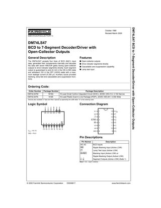
 DM74LS47 Truth Table Note 2: BI/RBO is wire-AND logic serving as blanking input (BI) and/or ripple-blanking output (RBO). The blanking out (BI) must be open or held at a HIGH level when output functions 0 through 15 are desired, and ripple-blanking input (RBI) must be open or at a HIGH level if blanking or a decimal 0 is not desired. X = input may be HIGH or LOW. Note 3: When a LOW level is applied to the blanking input (forced condition) all segment outputs go to a HIGH level regardless of the state of any other input condition. Note 4: When ripple-blanking input (RBI) and inputs A0, A1, A2 and A3 are LOW level, with the lamp test input at HIGH level, all segment outputs go to a HIGH level and the ripple-blanking output (RBO) goes to a LOW level (response condition). Note 5: When the blanking input/ripple-blanking output (BI/RBO) is OPEN or held at a HIGH level, and a LOW level is applied to lamp test input, all segment outputs go to a LOW level. Functional Description The DM74LS47 decodes the input data in the pattern indi- cated in the Truth Table and the segment identification illustration. If the input data is decimal zero, a LOW signal applied to the RBI blanks the display and causes a multi- digit display. For example, by grounding the RBI of the highest order decoder and connecting its BI/RBO to RBI of the next lowest order decoder, etc., leading zeros will be suppressed. Similarly, by grounding RBI of the lowest order decoder and connecting its BI/RBO to RBI of the next high- est order decoder, etc., trailing zeros will be suppressed. Leading and trailing zeros can be suppressed simulta- neously by using external gates, i.e.: by driving RBI of a intermediate decoder from an OR gate whose inputs are BI/RBO of the next highest and lowest order decoders. BI/ RBO also serves as an unconditional blanking input. The internal NAND gate that generates the RBO signal has a resistive pull-up, as opposed to a totem pole, and thus BI/ RBO can be forced LOW by external means, using wired- collector logic. A LOW signal thus applied to BI/RBO turns off all segment outputs. This blanking feature can be used to control display intensity by varying the duty cycle of the blanking signal. A LOW signal applied to LT turns on all segment outputs, provided that BI/RBO is not forced LOW. Decimal Inputs Outputs or Note Function LT RBI A3 A2 A1 A0 BI/RBO a b c d e f g 0 H H L L L L H L L L L L L H (Note 2) 1 H X L L L H H H L L H H H H (Note 2) 2 H X L L H L H L L H L L H L 3 H X L L H H H L L L L H H L 4 H X L H L L H H L L H H L L 5 H X L H L H H L H L L H L L 6 H X L H H L H H H L L L L L 7 H X L H H H H L L L H H H H 8 H X H L L L H L L L L L L L 9 H X H L L H H L L L H H L L 10 H X H L H L H H H H L L H L 11 H X H L H H H H H L L H H L 12 H X H H L L H H L H H H L L 13 H X H H L H H L H H L H L L 14 H X H H H L H H H H L L L L 15 H X H H H H H H H H H H H H BI X X X X X X L H H H H H H H (Note 3) RBI H L L L L L L H H H H H H H (Note 4) LT L X X X X X H L L L L L L L (Note 5)
  • 4. www.fairchildsemi.com 4 DM74LS47 Absolute Maximum Ratings(Note 6) Note 6: The “Absolute Maximum Ratings” are those values beyond which the safety of the device cannot be guaranteed. The device should not be operated at these limits. The parametric values defined in the Electrical Characteristics tables are not guaranteed at the absolute maximum ratings. The “Recommended Operating Conditions” table will define the conditions for actual device operation. Recommended Operating Conditions Note 7: OFF-State at a–g. Electrical Characteristics Over recommended operating free air temperature range (unless otherwise noted) Note 8: All typicals are at VCC = 5V, TA = 25°C. Note 9: Not more than one output should be shorted at a time, and the duration should not exceed one second. Switching Characteristics at VCC = +5.0V, TA = +25°C Note 10: LT = HIGH, A0–A3 = LOW Supply Voltage 7V Input Voltage 7V Operating Free Air Temperature Range 0°C to +70°C Storage Temperature Range −65°C to +150°C Symbol Parameter Min Nom Max Units VCC Supply Voltage 4.75 5 5.25 V VIH HIGH Level Input Voltage 2 V VIL LOW Level Input Voltage 0.8 V IOH HIGH Level Output Current −250 µA a − g @ 15V = VOH (Note 7) IOH HIGH Level Output Current BI /RBO −50 µA IOL LOW Level Output Current 24 mA TA Free Air Operating Temperature 0 70 °C Symbol Parameter Conditions Min Typ Max Units (Note 8) VI Input Clamp Voltage VCC = Min, II = −18 mA −1.5 V VOH HIGH Level VCC = Min, IOH = Max, 2.7 3.4 V Output Voltage VIL = Max, BI /RBO IOFF Output HIGH Current Segment Outputs VCC = 5.5V, VO = 15V a − g 250 µA VOL LOW Level VCC = Min, IOL = Max, 0.35 0.5 Output Voltage VIH = Min, a − g IOL = 3.2 mA, BI /RBO 0.5 V IOL = 12 mA, a –g 0.25 0.4 IOL = 1.6 mA, BI /RBO 0.4 II Input Current @ Max VCC = Max, VI = 7V 100 µA Input Voltage VCC = Max, VI = 10V IIH HIGH Level Input Current VCC = Max, VI = 2.7V 20 µA IIL LOW Level Input Current VCC = Max, VI = 0.4V −0.4 mA IOS Short Circuit VCC = Max (Note 9), mA Output Current IOS at BI/RBO −0.3 −2.0 ICC Supply Current VCC = Max 13 mA RL = 665Ω Symbol Parameter Conditions CL = 15 pF Units Min Max tPLH Propagation Delay 100 ns tPHL An to a –g 100 tPLH Propagation Delay 100 ns tPHL RBI to a –g (Note 10) 100
  • 5. 5 www.fairchildsemi.com DM74LS47 Physical Dimensions inches (millimeters) unless otherwise noted 16-Lead Small Outline Integrated Circuit (SOIC), JEDEC MS-012, 0.150 Narrow Package Number M16A
  • 6. www.fairchildsemi.com 6 DM74LS47BCDto7-SegmentDecoder/DriverwithOpen-CollectorOutputs Physical Dimensions inches (millimeters) unless otherwise noted (Continued) 16-Lead Plastic Dual-In-Line Package (PDIP), JEDEC MS-001, 0.300 Wide Package Number N16E Fairchild does not assume any responsibility for use of any circuitry described, no circuit patent licenses are implied and Fairchild reserves the right at any time without notice to change said circuitry and specifications. LIFE SUPPORT POLICY FAIRCHILD’S PRODUCTS ARE NOT AUTHORIZED FOR USE AS CRITICAL COMPONENTS IN LIFE SUPPORT DEVICES OR SYSTEMS WITHOUT THE EXPRESS WRITTEN APPROVAL OF THE PRESIDENT OF FAIRCHILD SEMICONDUCTOR CORPORATION. As used herein: 1. Life support devices or systems are devices or systems which, (a) are intended for surgical implant into the body, or (b) support or sustain life, and (c) whose failure to perform when properly used in accordance with instructions for use provided in the labeling, can be rea- sonably expected to result in a significant injury to the user. 2. A critical component in any component of a life support device or system whose failure to perform can be rea- sonably expected to cause the failure of the life support device or system, or to affect its safety or effectiveness. www.fairchildsemi.com