1. Power over Fiber – Printed Circuit Board (PCB) Project
Inbar Kinarty
The goal of this project was to design a printed circuit board (i.e PCB) for the Data acquisition
remote node powered over the communications optical fiber project made by Antonio J N Batista at
Instituto de Plasmas e Fusão Nuclear, Instituto Superior Técnico, Universidade de Lisboa, Portugal.
The PCB will perform in a harsh electromagnetic environment, close to the experimental
devices. Therefore, the motivation for the project was to have an architecture based on Power-over-
Fiber technology, and to replace the traditional copper cables and power supplies. The advantages of
an optical fiber in such an environment are that it is immune to electromagnetic noise and can supply
power to the remote node electronics. The architecture of the design uses a laser power convertor (an
array of photovoltaic cells) to convert the laser light into electricity. The power that is generated is
enough to power an ADC, a low power FPGA and an optical transmitter. The laser power convertor
is also used as a communication receiver and to recover the acquisition clock, this makes sure the
remote data acquisition nodes are synchronized.
Further explanation about the design, sketches and photos of the prototype can be found in the
corresponding article.
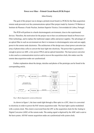
Fig 1. Block diagram for system architecture
As shown in figure 1, the laser sends light through a fiber optic to a LPC, there it is converted
to electricity in order to power the PoF remote acquisition node. The laser light is pulse modulated
with a system clock. This clock is recovered from the LPC as the acquisition clock for the Analog to
Digital Convertor (ADC) of the remote node. The analog signal is digitized by the ADC and is sent to
the host system. All PoF remote acquisition nodes are synchronized with system clock.
2. Fig 2. Prototype of the implementation
The need of this project was to design a board that will replace the prototype in figure 2. The
final result is presented in the figure 3.
Fig 3. Manufacture of top and bottom layers of the PCB –Final Version.
3. I started with a schematic that reflects the prototype presented in figure 3. This stage of the
design requires reading all the datasheets of the components, understanding the pin numbers
connection and find extra recommended connections (decoupling capacitor, what are their sizes,
voltage connections, etc.).
Fig 4. Schematic of the implementation as drawn in Orcad Design Entry CIS
After the schematic was ready, the next stage is to produce PCB footprints for each of the
component that will be used in the PCB design tool – Allegro. The footprints were mainly created
using the Footprint maker 0.0080 software. This software has a large number of predefined
footprints, and also allows the user to create their own by defining the measurements according to the
datasheets of the components that are used in the design. This stage requires to read and understand
the technical properties of several and different components and to read the datasheets correctly in
order to create a correct footprint.
Next, I design a 2 layers board, using the Allegro PCB editor, which will be manufactured at
IPFN. The board is presented in figures 5 and 6. While designing the board I had to take into
R1 1100
C42
1uF
GND
U8
LMP7717
1OUT_A
2-IN_A
3+IN_A
4V-
8 V+
7 OUT_B
6 -IN_B
5 +IN_B
GND
ADC_40MHz_CLK
GND
GND
GND
+IN_A
+IN_B
GND
GND
GND
GND
ADC_2MHz_CLK
D1
BZX84C10/SOT
ADC_40MHz_CLK
LPC1
PPC-6E
100K
3.3V
OUT_A
OUT_B R19 RESISTOR
R20 RESISTOR
C18
CAPACITOR
3.3V
L4 uH
L5 uH
3.3V
C19
CAPACITOR
AIN0P
AIN0N
3.3V
OUT_B
OUT_A
100K
ref _2MHz_CLK
Buck-Boost Convertors Power
3.3V
3.3V
3.3V
+IN_A+IN_A
+IN_B
+IN_A
C46 10n
+IN_B
3.3V
C47 100n
3.3V
U5
AGLN125V2
GND
1
IO82RSB1
2
IO81RSB1
3
IO80RSB1
4
IO79RSB1
5
IO78RSB1
6
IO77RSB1
7
IO76RSB1
8
GND
9
IO75RSB1
10
IO74RSB1
11
VCOMPLF
12
GEA0/IO72RSB1
13
VCCPLF
14
IO70RSB1
15
IO69RSB1
16
VCC
17
VCCIB1
18
IO68RSB1
19
IO67RSB1
20
IO66RSB1
21
IO65RSB1
22
IO64RSB1
23
VMV1
24
GNDQ
25
IO61RSB1
26
FF/IO60RSB1
27
IO59RSB1
28
IO58RSB1
29
IO57RSB1
30
IO56RSB1
31
IO55RSB1
32
IO54RSB1
33
IO53RSB1
34
IO52RSB1
35
IO51RSB1
36
VCC
37
GND
38
VCCIB1
39
IO49RSB1
40
IO47RSB1
41
IO46RSB1
42
IO45RSB1
43
IO44RSB1
44
IO43RSB1
45
IO42RSB1
46
TCK
47
TDI
48
TMS
49
VMV1
50
GND
51VPUMP
52NC
53TDO
54TRST
55VJTAG
56IO41RSB0
57IO40RSB0
58IO39RSB0
59IO38RSB0
60IO37RSB0
61IO36RSB0
62GDB0/IO34RSB0
63GDA0/IO33RSB0
64GDC0/IO32RSB0
65VCCIB0
66GND
67VCC
68IO31RSB0
69
IO29RSB0
71IO28RSB0
72IO27RSB0
73VMV0
74GNDQ
75
IO30RSB0
70
IO24RSB0
76IO23RSB0
77IO22RSB0
78IO21RSB0
79IO20RSB0
80IO19RSB0
81IO18RSB0
82IO17RSB0
83IO16RSB0
84IO15RSB0
85IO14RSB0
86VCCIB0
87GND
88VCC
89IO12RSB0
90IO10RSB0
91IO08RSB0
92IO07RSB0
93IO06RSB0
94IO05RSB0
95IO04RSB0
96IO03RSB0
97IO02RSB0
98IO01RSB0
99IO00RSB0
100
1.2V
1.2V
C2 1uF
C41
1uF
C1
1F - SuperCapacitor
3.3V 3.3V 3.3V 3.3V 3.3V
3.3V
3.3V
U7
ADS7945
GND 1
AVDD 2
REF 3
REFGND4
5AIN0P
6AIN0N
7AIN1N
AIN1P8
NC19
NC010
CH SEL11
PDEN12
/CS13
SCCLK14
SDO15
DVDD16
3.3V
3.3V
C45 0.1uF
3.3V
U9
REF5050
1DNC_1
2Vin
3TEMP
4GND
8 DNC_2
7 NC
6 Vout
5 TRIM/NR
U2
TPS63060
L1
1
Vin
2
EN
3
VAUX
6
PS/SYNC
4
L2
10
Vout
9
FB
8
PGND
7PG
5
D2
OPV314YAT
U1
TPS63000
L1
4
Vin
5
VinA
8
EN
6
PS/SYNC
7
GND
9
L2
2
Vout
1
FB
10
PGND
3
5.4V
ref _2MHz_CLK
REF
REF
C20100n
C2110n
C4
10uF
L2 1uH
C5
10uF C9
0.1uF
C44 0.1uF C10
22uF
ADC_2MHz_CLK
C11
22uF
R2
1M
ADC_Data
5.4V
C12
10pF
C22100n
R6
100K
C2310n
C7
10uF
C43
1uF
C8
22uF
C24100n
C2510n
Vin 5.4V
C26100n
J1
JTAG Header
1 2
3 4
5 6
7 8
9 10
C2710n
f p3_agl_tms
f p3_agl_tdo
f p3_agl_tck
f p3_agl_tdi
f p3_agl_trst
L1 2.2uH
5.4V
C3
10uF
R3
100
C28100n
C13
0.1uF
C2910n
1.2V
C30100n
PLL_Lock
TP1
TEST POINT
1
C3110n
fp3_agl_tms
fp3_agl_tdi
R4
1M
R7
180K
Manchester
C6
10uF
Manchester
chopper1
U6
TPS63000
L1
4
Vin
5
VinA
8
EN
6
PS/SYNC
7
GND
9
L2
2
Vout
1
FB
10
PGND
3
chopper2
L3 2.2uH
5.4V
C14
10uF
R10
100
C16
0.1uF
R11
270K
R12
200K
C15
10uF
1.2V
GND
C32100n
C3310n
C34100n
C3510n
C36100n
C3710n
5.4V
5.4V
C48
10uF
f p3_agl_tck
R15
1K
Vin
+
-
U4
LMV7219
5
3
4
2
1
R9 240
R14
1K
f p3_agl_trst
R13 39 f p3_agl_tdo
+
-
U3
OPA836
4
3
1
62
5
chopper2
chopper1
C38
470pF
R21 5
R2247
1.2V
GND
C39 1uF
C40 0.1uF
ADC_Data
GND
1.2V
R16
RESISTOR
C17
CAPACITOR
R17 RESISTOR
R18 RESISTOR
J2
CON6
1
2
3
4
5
6
AIN0N
AIN0P
J3
MAX4635EUB
1
2
3
4
5 6
7
8
9
10
GND
GND
C49
1uF
4. consideration some limitations (deriving mainly from the limitations of the machine that produces the
board):
1. Size of the board should remain as small as possible (although no specific restriction
was given).
2. The diameter of the via drills should be more than 0.6 mm.
3. The width of the copper lines should be more than 0.25 mm.
4. The spacing between elements should exceed 0.25 mm.
Fig 5. Top and bottom layers of the PCB – Version: POF_PROJECT_7.brd.
5. Fig 6. Manufacture of top and bottom layers of the PCB – Version: POF_PROJECT_7.brd.
After manufacturing the board, we tested the board gradually, and I had to solve several issues
in the design, until getting the final result. Several issues we found in the PCB prototype were:
1. When powering the board through the LPC, it doesn’t work properly (see open issues).
2. When powering the board with the transmitter, the power of the component that
supposed to give 5.4V, doesn’t reach this value.
3. The FPGA would not be programmed (see open issues).
4. Some pins were incorrect in the design; this caused the need to re-wire some pins.
We suspected that the problems above were driven from the mistakes made in the pins, and the
re-wiring of some components that brought noise to the board. We then decided to manufacture
a new design of the PCB, with all the corrections that I had to make.
The most updated version of the board is named: POF_PROJECT_14.brd. The final design of
the board that I made is presented in figures 6 and 7 below:
6. Fig 7. Top and bottom layers of the PCB – Version: POF_PROJECT_14.brd.
The final version of the PCB I made still need further testing and fixing some bugs.
Open Issues:
1. When powering the board using the LPC it did not work correctly. The LPC is pulsed,
and the charging time of the Super Capacitor is too slow for the TPS63060 to start
powering the rest of the components.
2. The FPGA could not be programed. Probably due to damage that was made when
removing it from the first prototype to the final board. A new FPGA should be soldered
for further testing of this issue.
3. Further testing need to be done in order to have the board fully functioning.