IBM Power Event, Keynote Presentation Doug DavisIBM Danmark
IBM Power Systems
Hvad er IBM's visioner med Smarter Computing?
Hvad er vores strategi for IBM Power-platformen? Få en "Trend & Directions"-præsentation fra lederen af vores Executive Briefing Center i Austin.
Doug Davies, Program Director, IBM
IBM is the first major storage vendor to deliver eMLC Flash Storage Systems and has been incorporating flash into its servers and storage products for many years. This presentation explains the benefits of using IBM FlashSystems with I/O Intensive workloads where lower latency can make the difference; use cases include Online Transaction processing (OLTP), Business Intelligence (BI), Online Analytical Processing (OLAP), Virtual Desktop Infrastructure (VDI), High Performance Computing (HPC), Content delivery solutions (such as cloud storage and video on demand).
During the last 100 years, information technology has moved from a specialized tool to a pervasive
influence on nearly every aspect of life. From tabulating machines that simply counted with mechanical
switches or vacuum tubes to the first programmable computers, IBM® has been a part of this growth,
while always helping customers to solve problems
To meet today's complex and ever-changing business demands, you need a
solid foundation of server, storage, networking and software resources that
is simple to deploy and can quickly and automatically adapt to changing
conditions. You also need access to—and the ability to take advantage
of—broad expertise and proven best practices in systems management,
applications, hardware maintenance and more.
IBM PureFlex System, an expert integrated system, offers a cloud-enabled integrated server, storage, and networking platform that delivers intelligent workload deployment and scalable IT resource pools. This IBM Redpaper describes disaster recovery strategies in the PureFlex System private cloud environment that is built with IBM SmartCloud Entry running on IBM x86 and IBM POWER compute nodes. For more information on Pure Systems, visit http://ibm.co/18vDnp6.
Visit the official Scribd Channel of IBM India Smarter Computing at http://bit.ly/VwO86R to get access to more documents.
This overview of IBM's PureSystems™ family will highlight how key components of IBM Flex System Solutions and PureFlex offerings can save you time and money with:
1. System availability
2. Power consumption
3. Virtualization
4. Multiple platforms and operating systems
PureSystems brings together built-in expertise, integrated components, and simplified management to take IT into the next decade. We think that deserves a sigh of relief, and so will you.
The Rico Board is an excellent high-performance Single Board Computer using the newest TI’s AM437x Sitara ARM Cortex-A9 based solution. It has 512MB DDR3, 4GB eMMC Flash, 16MB QSPI Flash and 32KB EEPROM on board, featuring various peripherals like Debug Serial, USB, Gigabit Ethernet, Dual-Camera, TF, HDMI, LCD and etc. It is preloaded with Linux and supplied with optional 7-inch LCD Module including capacitive touch screen. More information can be found at MYIR's website: http://www.myirtech.com/list.asp?id=510
Morello Technology Demonstrator Hardware Overview - Mark Inskip, ArmKTN
Presentation from the briefing event for ISCF Digital Security by Design competition: Technology Enabled Business-Led Demonstator Stage 1 Expression of Interest
Development Board for NXP i.MX 8M Quad Application ProcessorsLinda Zhang
The overview file introduces a versatile platform MYD-JX8MX development board for evaluating the MYC-JX8MX CPU Module. It takes full features of the i.MX 8M processor and has brought out rich peripherals through connectors and headers such as 4 x USB 3.0 Host ports and 1 x USB 3.0 Host/Device port, Gigabit Ethernet, TF card slot, USB based Mini PCIe interface for 4G LTE Module, WiFi/BT, Audio In/Out, HDMI, 2 x MIPI-CSI, MIPI-DSI, 2 x LVDS display interfaces, PCIe 3.0 (x4) NVMe SSD Interface, etc. The board is ready to run Linux and can work in extended temperature ranging from -30°C to 80°C. It is delivered with necessary cable accessories for customers to easily start development as soon as getting it out-of-box. A MIPI Camera Module MY-CAM003 is provided as an option for the board.
Jetson AGX Xavier and the New Era of Autonomous MachinesDustin Franklin
Deep-dive on NVIDIA Jetson AGX Xavier, designed to help you deploy advanced AI onboard robots, drones, and other autonomous machines. View the webinar here: https://bit.ly/2BWVWv1
The MYD-YA15XC-T development board is using the MYC-YA15XC-T CPU Module as core controller board which is populated on a specially designed base board through 1.0 mm pitch 148-pin stamp-hole (Castellated-Hole) expansion interface. The MYD-YA15XC-T is a good reference design for using ST STM32MP1 Processors which features 650MHz Single or Dual Arm Cortex-A7 and 209MHz Cortex-M4 Cores. Typical applications are industrial control, consumer electronics, smart home, medical and more other energy-efficient applications which require rich performance and low power. More information can be found at:
http://www.myirtech.com/list.asp?id=659
The MYS-8MMX Single Board Computer has a compact design with only 95mm by 65mm form factor. It is powered by NXP’s first embedded multicore applications processor i.MX 8M Mini which features up to 1.8GHz quad-core ARM Cortex-A53 plus 400MHz Cortex-M4 processor. The tiny board takes full features of the processor and is equipped with 2GB DDR4, 8GB eMMC and 32MB QSPI Flash. It has explored rich peripheral interfaces through headers and connectors including two USB 2.0 Host, one USB OTG, one Gigabit Ethernet, TF card, M.2 interface, LVDS LCD interface, MIPI CSI interface, HDMI output, IO expansion interface and more others. The AP6256 WiFi/BT module on the board also allows wireless communications with other devices. It is capable of running Linux operating system based on the Yocto 3.0 or Ubuntu 18.04 .
LF Energy Webinar: Electrical Grid Modelling and Simulation Through PowSyBl -...DanBrown980551
Do you want to learn how to model and simulate an electrical network from scratch in under an hour?
Then welcome to this PowSyBl workshop, hosted by Rte, the French Transmission System Operator (TSO)!
During the webinar, you will discover the PowSyBl ecosystem as well as handle and study an electrical network through an interactive Python notebook.
PowSyBl is an open source project hosted by LF Energy, which offers a comprehensive set of features for electrical grid modelling and simulation. Among other advanced features, PowSyBl provides:
- A fully editable and extendable library for grid component modelling;
- Visualization tools to display your network;
- Grid simulation tools, such as power flows, security analyses (with or without remedial actions) and sensitivity analyses;
The framework is mostly written in Java, with a Python binding so that Python developers can access PowSyBl functionalities as well.
What you will learn during the webinar:
- For beginners: discover PowSyBl's functionalities through a quick general presentation and the notebook, without needing any expert coding skills;
- For advanced developers: master the skills to efficiently apply PowSyBl functionalities to your real-world scenarios.
UiPath Test Automation using UiPath Test Suite series, part 3DianaGray10
Welcome to UiPath Test Automation using UiPath Test Suite series part 3. In this session, we will cover desktop automation along with UI automation.
Topics covered:
UI automation Introduction,
UI automation Sample
Desktop automation flow
Pradeep Chinnala, Senior Consultant Automation Developer @WonderBotz and UiPath MVP
Deepak Rai, Automation Practice Lead, Boundaryless Group and UiPath MVP
GDG Cloud Southlake #33: Boule & Rebala: Effective AppSec in SDLC using Deplo...James Anderson
Effective Application Security in Software Delivery lifecycle using Deployment Firewall and DBOM
The modern software delivery process (or the CI/CD process) includes many tools, distributed teams, open-source code, and cloud platforms. Constant focus on speed to release software to market, along with the traditional slow and manual security checks has caused gaps in continuous security as an important piece in the software supply chain. Today organizations feel more susceptible to external and internal cyber threats due to the vast attack surface in their applications supply chain and the lack of end-to-end governance and risk management.
The software team must secure its software delivery process to avoid vulnerability and security breaches. This needs to be achieved with existing tool chains and without extensive rework of the delivery processes. This talk will present strategies and techniques for providing visibility into the true risk of the existing vulnerabilities, preventing the introduction of security issues in the software, resolving vulnerabilities in production environments quickly, and capturing the deployment bill of materials (DBOM).
Speakers:
Bob Boule
Robert Boule is a technology enthusiast with PASSION for technology and making things work along with a knack for helping others understand how things work. He comes with around 20 years of solution engineering experience in application security, software continuous delivery, and SaaS platforms. He is known for his dynamic presentations in CI/CD and application security integrated in software delivery lifecycle.
Gopinath Rebala
Gopinath Rebala is the CTO of OpsMx, where he has overall responsibility for the machine learning and data processing architectures for Secure Software Delivery. Gopi also has a strong connection with our customers, leading design and architecture for strategic implementations. Gopi is a frequent speaker and well-known leader in continuous delivery and integrating security into software delivery.
Accelerate your Kubernetes clusters with Varnish CachingThijs Feryn
A presentation about the usage and availability of Varnish on Kubernetes. This talk explores the capabilities of Varnish caching and shows how to use the Varnish Helm chart to deploy it to Kubernetes.
This presentation was delivered at K8SUG Singapore. See https://feryn.eu/presentations/accelerate-your-kubernetes-clusters-with-varnish-caching-k8sug-singapore-28-2024 for more details.
Dev Dives: Train smarter, not harder – active learning and UiPath LLMs for do...UiPathCommunity
💥 Speed, accuracy, and scaling – discover the superpowers of GenAI in action with UiPath Document Understanding and Communications Mining™:
See how to accelerate model training and optimize model performance with active learning
Learn about the latest enhancements to out-of-the-box document processing – with little to no training required
Get an exclusive demo of the new family of UiPath LLMs – GenAI models specialized for processing different types of documents and messages
This is a hands-on session specifically designed for automation developers and AI enthusiasts seeking to enhance their knowledge in leveraging the latest intelligent document processing capabilities offered by UiPath.
Speakers:
👨🏫 Andras Palfi, Senior Product Manager, UiPath
👩🏫 Lenka Dulovicova, Product Program Manager, UiPath
The Art of the Pitch: WordPress Relationships and SalesLaura Byrne
Clients don’t know what they don’t know. What web solutions are right for them? How does WordPress come into the picture? How do you make sure you understand scope and timeline? What do you do if sometime changes?
All these questions and more will be explored as we talk about matching clients’ needs with what your agency offers without pulling teeth or pulling your hair out. Practical tips, and strategies for successful relationship building that leads to closing the deal.
"Impact of front-end architecture on development cost", Viktor TurskyiFwdays
I have heard many times that architecture is not important for the front-end. Also, many times I have seen how developers implement features on the front-end just following the standard rules for a framework and think that this is enough to successfully launch the project, and then the project fails. How to prevent this and what approach to choose? I have launched dozens of complex projects and during the talk we will analyze which approaches have worked for me and which have not.
GraphRAG is All You need? LLM & Knowledge GraphGuy Korland
Guy Korland, CEO and Co-founder of FalkorDB, will review two articles on the integration of language models with knowledge graphs.
1. Unifying Large Language Models and Knowledge Graphs: A Roadmap.
https://arxiv.org/abs/2306.08302
2. Microsoft Research's GraphRAG paper and a review paper on various uses of knowledge graphs:
https://www.microsoft.com/en-us/research/blog/graphrag-unlocking-llm-discovery-on-narrative-private-data/
Search and Society: Reimagining Information Access for Radical FuturesBhaskar Mitra
The field of Information retrieval (IR) is currently undergoing a transformative shift, at least partly due to the emerging applications of generative AI to information access. In this talk, we will deliberate on the sociotechnical implications of generative AI for information access. We will argue that there is both a critical necessity and an exciting opportunity for the IR community to re-center our research agendas on societal needs while dismantling the artificial separation between the work on fairness, accountability, transparency, and ethics in IR and the rest of IR research. Instead of adopting a reactionary strategy of trying to mitigate potential social harms from emerging technologies, the community should aim to proactively set the research agenda for the kinds of systems we should build inspired by diverse explicitly stated sociotechnical imaginaries. The sociotechnical imaginaries that underpin the design and development of information access technologies needs to be explicitly articulated, and we need to develop theories of change in context of these diverse perspectives. Our guiding future imaginaries must be informed by other academic fields, such as democratic theory and critical theory, and should be co-developed with social science scholars, legal scholars, civil rights and social justice activists, and artists, among others.
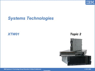
{DESCRIPTION} This is the title slide. There in an image of some System x servers in the bottom right corner. {TRANSCRIPT} Welcome to Systems Technologies. This is the second module in the IBM Technical Principles course XTW01.
{DESCRIPTION} This slide presents a bulleted list of this courses objectives {TRANSCRIPT} Upon completion of this module you will be familiar with : The buses found in, the memory technologies used, the processors employed in System x servers We will also discuss the disk technologies and network technologies used in System x servers
{DESCRIPTION} This slide presents a bulleted list of the technologies discussed in this topic. {TRANSCRIPT} In this section we will discuss system buses .
{DESCRIPTION} This slide presents a bulleted list of the topics that will be discussed in this section. There is an image of a bus transportation vehicle in the bottom right corner. {TRANSCRIPT} The term bus draws to mind an image of the local metro transportation. With regard to computer buses the analogy is quite accurate. Just as a metro bus moves people between points in a city, a bus in a computer system is used to move signaling of like kind between points within a computer system. In this section we will review the history of bus architecture and discuss the various buses within a computer system.
{DESCRIPTION} This slide presents a bulleted list of the technologies discussed in this topic. {TRANSCRIPT} In this section we will discuss memory .
{DESCRIPTION} A TEST {TRANSCRIPT} Two types of memory are utilized in a micro computer today; volatile, whose content is quickly changed, but will be lost upon loss of power and non-volatile, which is slower but once programmed will retain its content even if power is removed. Generally volatile memory is used as main system memory, whereas non-volatile is used for the storage of system and adapter initialization code or BIOS and firmware. Volatile memory employs two design methodologies, static which is fast, more complex and more expensive, and dynamic which is slower, fabricated more easily, is less costly but incurs a performance overhead due to it requiring additional read operations to refresh its contents. Main system memory is typically dynamic, with static memory being used where performance is of prime concern. Non-volatile memory used in microcomputers today also employs two design methodologies termed NAND and NOR, the NAND having better speed characteristics such that it has begun to be utilized as a replacement for mass storage as it does not suffer the mechanical issues imposed on hard disk drives. The NOR variety being typically used for system firmware. In this section we will review basic memory operation, its technologies and its usage in System x Servers.
{DESCRIPTION} This slide presents a bulleted list of the technologies discussed in this topic. {TRANSCRIPT} In this section we will discuss processors .
{DESCRIPTION} A TEST {TRANSCRIPT} Processors architecture has changed radically in recent years, providing greater power, increased memory capacities, and lower energy utilization. In this section we will review the processor families currently utilized in IBM System x servers.
{DESCRIPTION} This slide presents bulleted list of the Celeron G1100 features. There is an image of its functional block diagram on the right and a Celeron inside logo at the bottom left. {TRANSCRIPT} The Celeron G series, employs the Nehalem architecture which was introduced with the Core i7 desktop processor. This architecture integrates of most functionality of the now defunct Northbridge chip, particularly the memory controller into the processor itself. It employs multiple processor cores, each having a L2 cache and a L3 cache shared amongst them. Nehalem introduced the QuickPath interconnect and several features to reduce power consumption. The Celeron G1100 utilizes two dies interconnected via QPI on one substrate. The core die, employs two processor cores, each with 256KBs L2 cache and a single shared 2MB L3 cache. The uncore die hosts a 2 channel DDR3 memory controller, which supports 2 UDIMMs at up to 1066 MT/s per channel. It does not support ECC. ECC functionality is present in the processor, but is disabled by default. When paired with a 3400 series Periphiel Controller Hub (PCH), ECC functionality is enabled during boot by utilizing dynamic fusing. During boot the PCH sends a fuse override request to the processor via the DMI, a Proprietary x4 PCI-E, interface. The processor executes internal p-code to change the state of the fuse which enables ECC. The Celeron G presents 16 lanes of PCI-E at 5.0 GT/s per lane. This interface maybe configured as one x16 or two x8 interfaces. The DMI interface is utilized to interface with the system chip set or PCH. Additionally the processor hosts a graphics processor unit.
{DESCRIPTION} This slide presents a bulleted list of the key technologies employed in the Celeron G processor. There is an image of a Celeron processor in the right upper corner and a Celeron inside logo in the bottom left. {TRANSCRIPT} Intel processors employ techniques to enhance throughput and energy conservation. In the case of the Celeron G processor , these include. Intel® Virtualization Technology (VT-x) - created a new processor execution mode (root) the virtual machine manager (VMM) runs in. It allows the VMM to execute privileged instructions disallowed by processors without VT-x. Additionally it enhances the isolation that must be maintained between guest OS’s. Intel® 64 - architecture delivers 64-bit computing and improves performance by allowing systems to address more than 4GB of both virtual and physical memory. Idle States - allows the processor to disable specific functionality based on utilization, thereby reducing energy consumed. Enhanced Intel SpeedStep® Technology - The cores operating frequency and voltage can be lowered to reduce power consumption. Execute Disable Bit - a hardware-based security feature that can reduce exposure to viruses and malicious-code attacks and prevent harmful software from executing and propagating.
{DESCRIPTION} This slide presents bulleted list of the Pentium G6950 features. There is an image of its functional block diagram on the right and a Pentium inside logo at the bottom left. {TRANSCRIPT} The Pentium G series, also employs the Nehalem architecture. The core die, employs two processor cores, each with 256KBs L2 cache and a single 3MB L3 cache shared amongst them. The “uncore” die hosts a 2 channel DDR3 memory controller, which supports 2 UDIMMs at up to 1066 MT/s per channel. It does not support ECC. ECC functionality is present in the processor, and is enabled when the processor is paired with a 3400 series PCH as with the Celeron G. The Pentium G presents 16 lanes of PCI-E at 5.0 GT/s per lane. This interface maybe configured as one x16 or two x8 interfaces. DMI is utilized to interface with the Peripheral Controller Hub (PCH) Additionally it hosts a graphics processor unit..
{DESCRIPTION} This slide presents a bulleted list of the key technologies employed in the Pentium G processor. There is an image of a Pentium processor in the right upper corner and a Pentium inside logo in the bottom left. {TRANSCRIPT} These are the technologies supported with the Pentium G processor.
{DESCRIPTION} This slide presents bulleted list of the Core i3 500 series features. There is an image of its functional block diagram on the right and a Core i3 inside logo at the bottom left. {TRANSCRIPT} The Core i3 series, also employs the Nehalem architecture. The core die, employs two processor cores, each with 256KBs L2 cache and a single 4MB L3 cache shared amongst them. The “uncore” die hosts a 2 channel DDR3 memory controller, which supports 2 UDIMMs at up to 1333 MT/s per channel. It does not support ECC. ECC functionality is implemented as with the Celeron G and Pentium G. The Core i3 presents 16 lanes of PCI-E at 5.0 GT/s per lane. This interface maybe configured as one x16 or two x8 interfaces. DMI is utilized to interface with the system chip set or Peripheral Controller Hub (PCH) Additionally its hosts a graphics processor unit.
{DESCRIPTION} This slide presents a bulleted list of the key technologies employed in the Core i3 processor. There is an image of a Core i3 processor in the right upper corner and a Core i3 inside logo in the bottom left. {TRANSCRIPT} These are the technologies supported with the Core i3 processor. Added to the Core i3 is: Intel® Hyper-Threading Technology - delivers thread-level parallelism on each core resulting in more efficient use of core resources, higher processing throughput, and improved performance on multi-threaded software.
{DESCRIPTION} This slide presents bulleted list of the Xeon 3400 features. There is an image of its functional block diagram on the right and a Xeon inside logo at the bottom left. {TRANSCRIPT} The Xeon 3400 series, employs the Nehalem architecture. It is a single die device, employing four processor cores, each with 256KBs L2 cache and a single 8MB L3 cache shared amongst them. The die hosts a 2 channel DDR3 memory controller, which supports 3 RDIMMs or 2 UDIMMs per channel. It supports ECC. It presents 16 lanes of PCI-E at 5.0 GT/s per lane. This interface maybe configured as one x16 or two x8 or four x4 interfaces. DMI is utilized to interface with the PCH.
{DESCRIPTION} This slide presents a bulleted list of the key technologies employed in the Xeon 3400 processor. There is an image of a Xeon processor in the right upper corner and a Xeon inside logo in the bottom left. {TRANSCRIPT} The Xeon 3000 series employs these technologies. Those we haven’t discussed include: Intel® Virtualization Technology for Directed I/O (VT-d) - extends Intel's Virtualization Technology support for IA-32 (VT-x) by adding new support for I/O-device virtualization. Intel® Trusted Execution Technology - provides hardware-based mechanisms that help protect against software-based attacks and protects the confidentiality and integrity of data. It does this by enabling an environment where applications can run within their own space, protected from all other software on the system. These capabilities provide the protection mechanisms, rooted in hardware, that are necessary to provide trust in the application's execution environment. In turn, this can help to protect vital data and processes from being compromised by malicious software running on the platform. Intel® Demand Based Switching - in which the applied voltage and clock speed of a processor core are kept at the minimum necessary levels for optimal performance of required operations. The core operates at a reduced voltage and clock speed until more processing power is required. This is achieved by monitoring the core’s use by application-level workloads, reducing the CPU speed when it is running idle while increasing it as the load increases.
{DESCRIPTION} This slide presents images of the of the Intel Xeon 5500 and 5600 series processors. It bullets the technologies employed in the Intel Xeon 5500 and 5600 series processors. {TRANSCRIPT} The Xeon 5500 series, employs the Nehalem-EP architecture. It is a single die device, employing four processor cores, each with 256KBs L2 cache and a shared 4or 8MB L3 cache dependant on processor. The die hosts a 3 channel DDR3 memory controller, which supports 3 RDIMMs or 2 UDIMMs per channel. It supports ECC. QPI is implemented as an external interface to the PCH and to interconnect processors in a SMP environment. Two QPI ports are available. Transfer rates are 4.8, 5.86, or 6.4GT/s dependant upon the processor. The Xeon 5600 series processor implements four or six independent processor cores on one silicon die utilizing a 32 nm process. This step in lithography bears the code name Westmere-EP. It employs all the technologies introduced by the Xeon 5500 processor. In addition to the increased core count, the L3 cache has been increased to 12MBs, it supports both 1.5v and 1.35v RDIMMs, and includes technologies to further reduce power consumption. New with the 5000 series is Intelligent Power Technology. When not in use an entire processor core can be idled and its power consumption reduced to near-zero independent from other operating cores thereby reducing idle state power consumption by up to 50 percent. This feature can be engaged automatically by the processor or controlled by the operation system or systems management. Westmere extends this capability to the “uncore” regions of the processor.
{DESCRIPTION} This slide presents a bulleted list of processor features. There is an image of an Opteron die. {TRANSCRIPT} The AMD Opteron 6100 series processors employ two, quad or six core 45nm process dies on one substrate, to provide 8 or 12 core functionality at speeds of up to 2.8GHz. The 6100 Series employs 2 - 64KB L1 caches, one parity protected for instructions, the other ECC protected for data, and a 512KB ECC protected L2 cache, per processor core. 2 - 6MB caches on each die are combined to implement a 12MB L3 cache that is shared between cores. The processors integrated memory controller provides 4 DDR3 low voltage (1.35v - 1.5v) memory channels, operating at up to 1333MT/s, supporting three registered DIMMs or 2 unbuffered DIMMs per channel. The processor employs HyperTransport 3 as a processor to processor / processor to I/O interconnect/link. HyperTransport 3 supports: PCI Express mapping: hardware translation of PCI-E data formats to HyperTransport data formats increases throughput between I/O, processors and memory. AC operating mode: allows the HyperTransport bus to achieve longer distances. In addition to chip to chip interconnection HyperTransport may be used to directly access adapters, ancillary PC boards, backplanes and other servers. Link splitting : the 16-bit link path may be utilized as two separate 8-bit links. This affords the ability to interconnect a larger number of devices without the use of additional hardware. Hot Plugging : HyperTransport devices (less CPU) may be installed and removed with the bus running. Dynamic Link Clock/Width Adjustment: allows the CPU to change the clock and the number of bits that are transmitted per clock cycle dynamically thereby reducing power consumption. HT Assist when enabled utilizes 1MB in each of the 2 L3 caches as a probe filter which creates a directory to track cache lines utilized by each CPU core. Should a CPU require data targeted in the L2 cache of another core the requester queries a CPU which in turn queries the L3 cache to identify the CPU which currently maintains the cached data. It then queries the appropriate CPU which passes the data to the requesting CPU. This methodology greatly reduces the number of query transactions that would need to occur e.g. query each CPU core to determine whether it hosted the data, validate it, then transfer it to the requester. Measurements have shown the utilization of HT Assist improves memory bandwidth by nearly 60%. The Opteron 6100 processor also supports: AMD Virtualization ™ or AMD-V ™ utilizes processor instruction extensions to facilitate the development of more efficient, secure and robust software for system virtualization. These extensions remove the overheads associated with software-only virtualization solutions and attempt to reduce the performance gap between virtualized and non-virtualized systems. The hypervisor uses these processor extensions to intercept and emulate privileged operations in the virtualized or guest OS. To maximize power utilization and cooling efficiencies, the Opteron 6100 processor also supports: C1E Power State: a sleep state, invoked when all processor cores are idle, which turns off memory controllers and HyperTransport 3 links. AMD Cool Speed technology: which r educes the frequency and voltage operating point (p-state) when a temperature limit is reached, thereby reducing peak thermal load, and power utilization. This results in energy cost savings by reducing power used to power the server and to cool the server environment. The Advanced Platform Management Link (APML): a SMBus v2.0 compatible 2-wire interface. APML is also referred to as the sideband interface (SBI). APML is used to communicate with the Remote Management and Temperature Sensor Interfaces. The processor is a SMBus slave; platform Baseboard Management Controllers may master the APML interface to read and write limited p-states to perform power management and RAS operations. AMD CoolCore ™ Technology: which reduces energy consumption by turning off unused parts of the processor AMD Smart Fetch Technology: which reduces power consumption by allowing idle cores to enter a "halt" state, causing them to draw less power during processing idle times, without compromising system performance Independent Dynamic Core Technology: which enables a variable clock frequency for each core, depending on the specific performance requirement of the applications it is supporting, which reduces power consumption. Dual Dynamic Power Management™ (DDPM™) Technology: provides an independent power supply to the cores and to the memory controller, allowing the cores and memory controller to operate on different voltages, depending on their usage. AMD PowerCap Manager: places a cap on the P-state level of a core via the BIOS which delivers consistent, predictable power consumption by the system.
{DESCRIPTION} This screen displays a topology of the processor-core and un-core illustrating the connection of the 8-cores, 24MB shared cache, and two integrated Memory controllers with bi-directional arrows pointing (blue) to the SMI links and yellow to the QPI links. {TRANSCRIPT} The Xeon 6500 / 7500 series, employs the Nehalem-EX architecture. It is a single die 45nm device, employing four, six or eight processor cores, each with 256KBs L2 cache and a shared 12, 18 or 24MB L3 cache dependant on processor. The die hosts 2 memory controllers each employing Symmetrical Memory Interfaces (SMI), ports between the processor and Scalable Memory Buffers (SMB). The ports associated with each memory controller operate in lock-step, each memory operation involves 2 data words and 2 ECC bytes. The SMB provides 2 DDR3 channels supporting 2 DIMMs each. QPI is implemented as an external interface to the PCH and to interconnect processors in a SMP environment. 4 QPI links are available. Transfer rates are 4.8, 5.86, or 6.4GT/s dependant upon the processor. The 6500 supports 2 way SMP, the 7500 4 or 8 way. It implements those technologies present in the Nehalem-EP
{DESCRIPTION} This slide presents a bulleted list of the technologies discussed in this topic. {TRANSCRIPT} In this section we will discuss disk subsystems .
{DESCRIPTION} A TEST {TRANSCRIPT} The Small Computer Systems Interface (SCSI) had been the mainstay of server disk I/O interfaces for over three decades. Technological advances and methodologies made over its lifetime, in an attempt to minimalize the I/O bottleneck inherent a hard disks mechanical nature, have been implemented throughout computer architecture. Methodologies such as caching, command queveing, LVDS, DDR, Redundancy, hot plugability were first implemented in disk I/O based upon SCSI. Both an internal and external parallel interface bus, SCSI designers found themselves impeded by the very constraints we discussed in the section on buses. In essence how to insure signaling integrity over a length of a group of wires at ever increasing clock speeds. The solution in the external space ultimately became Fibre Channel, though SCSI maintained its presence in the internal mass storage space. In the Desktop arena, SCSI was utilized only in unique applications, there seemed no real need for its hard disks ruggedized mechanicals, its caching methodologies and the added costs, but desktop designers in the pursuit of faster transfer rates were beginning to face the very same obstacles with their disk I/O interface of choice the Advanced Technology Attachment (ATA),. Their solution a serial interface with a fewer number of wires, and increased clock rate, the Serial Advanced Technology Attachment interface (SATA). Having opportunity with the definition of a new standard, features implemented by SCSI such and command queveing and hot plugability were included in SATA’s design. The performance of SCSI in terms of I/O bandwidth until recently with the advent of the SATA 3.0 standard was much greater then that of SATA, so there was resistance to the adoption of the interface in server designs. The erroneous perception SATA hard drives were less reliable then SCSI also lent to the latency in its acceptance, but eventually SATA replaced SCSI as the interface/drive of choice in the server arena. SATA did not implement all of the features present with SCSI, in particular its command set, which impacted systems performance so in 2003 Serial Attached SCSI (SAS) was introduced. It fully implements the features which were present with SCSI, adds some new ones, and provides the advantages of the serial interface. In this topic we will examine SATA and SAS and there utilization in System x servers.
{DESCRIPTION} This slide presents a bulleted list of the technologies discussed in this topic. {TRANSCRIPT} In this section we will discuss Networking .
{DESCRIPTION} A TEST {TRANSCRIPT} The networking content of this course is still under development.
{DESCRIPTION} This is the summary slide. It contains a bullet list outlining the goals of this course module. {TRANSCRIPT} Having completed this course module you should: Have a firm understanding of the various system buses and interconnects, and the role they play in server architecture. Have a clear understanding of memory architecture, the reasoning for and need to follow certain population rules when adding memory. Be familiar with the various processors offered with IBM System x Servers. Understand the disk subsystems used in servers today.
{DESCRIPTION} This slide presents a bulleted list of terms used in this course module. {TRANSCRIPT} Listed here and on the following two pages are the acronyms used in this course module.
{DESCRIPTION} This slide presents a bulleted list of terms used in this course module. {TRANSCRIPT} This is page two of three containing the acronyms used in this course module.
{DESCRIPTION} This slide presents a bulleted list of terms used in this course module. {TRANSCRIPT} This is page three of three containing the acronyms used in this course module.
{DESCRIPTION} Displays the statement of “End of Presentation” in the center of the slide. {TRANSCRIPT} Thank you. This concludes Topic 2 of IBM System x Technical Principles - Systems Technologies .