VLSI Design and Fabrication
• An Overview of Very Large Scale Integration
• Presented by: [Your Name]
• Date: [Date]
Introduction to VLSI
• • VLSI (Very Large Scale Integration) integrates
millions of transistors on a chip.
• • Powers compact, high-performance
electronics.
• • Evolution: SSI → MSI → LSI → VLSI → ULSI.
VLSI Design Flow
• 1. Specification
• 2. Architecture Design
• 3. RTL Design (HDL)
• 4. Logic Synthesis
• 5. Verification & Simulation
• 6. Physical Design
• 7. Fabrication
• 8. Testing & Packaging
Design Domains
• • Behavioral Domain – Algorithm-level design
• • RTL Domain – Register Transfer Level
• • Gate Level – Logic gates
• • Layout Level – Mask layout
Fabrication Process Overview
• 1. Wafer Preparation
• 2. Oxidation
• 3. Photolithography
• 4. Etching
• 5. Doping (Ion Implantation)
• 6. Metallization
• 7. Packaging
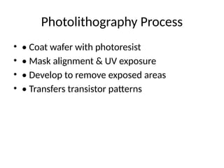
Photolithography Process
• • Coat wafer with photoresist
• • Mask alignment & UV exposure
• • Develop to remove exposed areas
• • Transfers transistor patterns
CMOS Technology
• • Uses NMOS and PMOS
• • Low power and high noise immunity
• • Ideal for scaling and integration
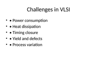
Challenges in VLSI
• • Power consumption
• • Heat dissipation
• • Timing closure
• • Yield and defects
• • Process variation
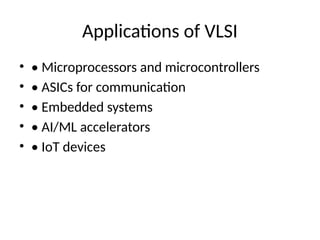
Applications of VLSI
• • Microprocessors and microcontrollers
• • ASICs for communication
• • Embedded systems
• • AI/ML accelerators
• • IoT devices
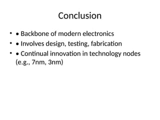
Conclusion
• • Backbone of modern electronics
• • Involves design, testing, fabrication
• • Continual innovation in technology nodes
(e.g., 7nm, 3nm)

VLSI_Design_and_Fabrication_Presentation.pptx

  • 1.
    VLSI Design andFabrication • An Overview of Very Large Scale Integration • Presented by: [Your Name] • Date: [Date]
  • 2.
    Introduction to VLSI •• VLSI (Very Large Scale Integration) integrates millions of transistors on a chip. • • Powers compact, high-performance electronics. • • Evolution: SSI → MSI → LSI → VLSI → ULSI.
  • 3.
    VLSI Design Flow •1. Specification • 2. Architecture Design • 3. RTL Design (HDL) • 4. Logic Synthesis • 5. Verification & Simulation • 6. Physical Design • 7. Fabrication • 8. Testing & Packaging
  • 4.
    Design Domains • •Behavioral Domain – Algorithm-level design • • RTL Domain – Register Transfer Level • • Gate Level – Logic gates • • Layout Level – Mask layout
  • 5.
    Fabrication Process Overview •1. Wafer Preparation • 2. Oxidation • 3. Photolithography • 4. Etching • 5. Doping (Ion Implantation) • 6. Metallization • 7. Packaging
  • 6.
    Photolithography Process • •Coat wafer with photoresist • • Mask alignment & UV exposure • • Develop to remove exposed areas • • Transfers transistor patterns
  • 7.
    CMOS Technology • •Uses NMOS and PMOS • • Low power and high noise immunity • • Ideal for scaling and integration
  • 8.
    Challenges in VLSI •• Power consumption • • Heat dissipation • • Timing closure • • Yield and defects • • Process variation
  • 9.
    Applications of VLSI •• Microprocessors and microcontrollers • • ASICs for communication • • Embedded systems • • AI/ML accelerators • • IoT devices
  • 10.
    Conclusion • • Backboneof modern electronics • • Involves design, testing, fabrication • • Continual innovation in technology nodes (e.g., 7nm, 3nm)