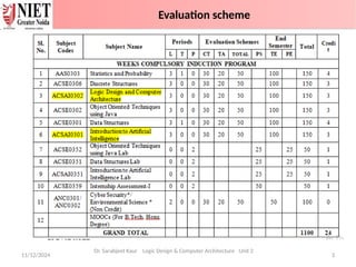
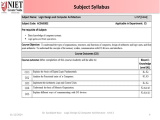
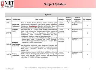
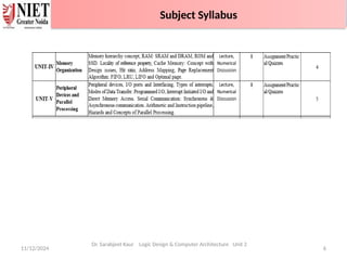
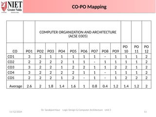
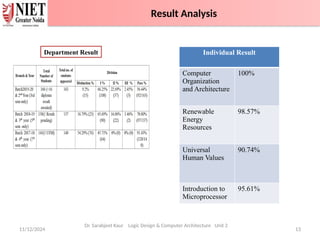
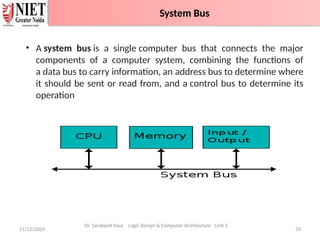
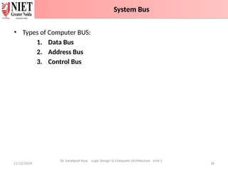
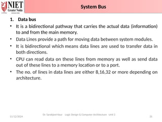
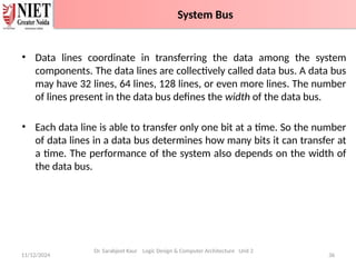
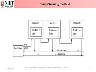
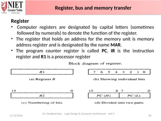
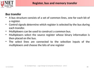
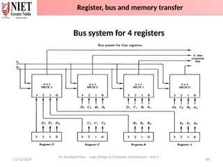
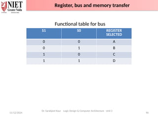
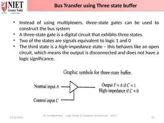
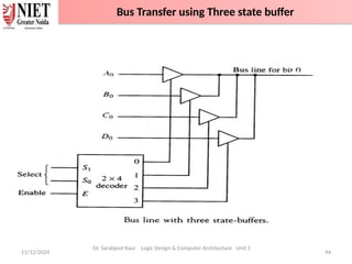
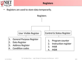
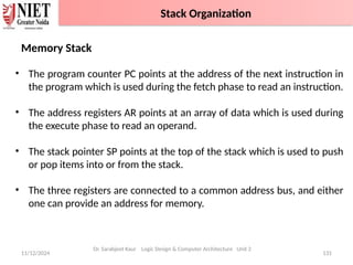
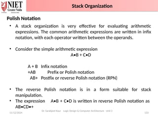
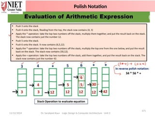
The document provides a comprehensive overview of a course on Logic Design and Computer Architecture, taught by Dr. Sarabjeet Kaur at the Noida Institute of Engineering and Technology. It covers essential topics such as computer organization, functional units, memory systems, and buses, along with course objectives and outcomes. Additionally, it outlines the relevance of this knowledge in various applications such as data science, high performance computing, and software optimization.


![11/12/2024 96
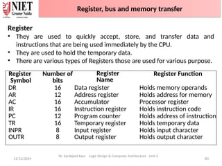
Most of the standard notations used for specifying operations on
memory transfer are stated below.
• The transfer of information from a memory unit to the user end is
called a Read operation.
• A memory word is designated by the letter M.
• We must specify the address of memory word while writing the
memory transfer operations.
• The address register is designated by AR and the data register by DR.
• Thus, a read operation can be stated as:
Read: DR ← M [AR]
• The Read statement causes a transfer of information into the data
register (DR) from the memory word (M) selected by the address
register (AR).
Dr. Sarabjeet Kaur Logic Design & Computer Architecture Unit 2
Memory Transfer](https://image.slidesharecdn.com/unit2ldcacs-241112135915-7103c9ca/85/Unit_2_LDCA_CS-Computer-Basics-pptx-96-320.jpg)
![11/12/2024 97
• The transfer of new information to be stored in the memory is called
a Write operation.
• The Write statement causes a transfer of information from register
R1 into the memory word (M) selected by address register (AR).
• Write: M [AR] ← R1
Dr. Sarabjeet Kaur Logic Design & Computer Architecture Unit 2
Memory Transfer](https://image.slidesharecdn.com/unit2ldcacs-241112135915-7103c9ca/85/Unit_2_LDCA_CS-Computer-Basics-pptx-97-320.jpg)
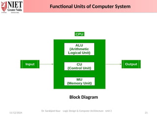
![11/12/2024 98
Memory Transfer Block diagram
Above Diagram showing connections to memory unit.
Write: M[AR] ← DR
Read: DR ← M[AR]
Dr. Sarabjeet Kaur Logic Design & Computer Architecture Unit 2
Memory Transfer](https://image.slidesharecdn.com/unit2ldcacs-241112135915-7103c9ca/85/Unit_2_LDCA_CS-Computer-Basics-pptx-98-320.jpg)
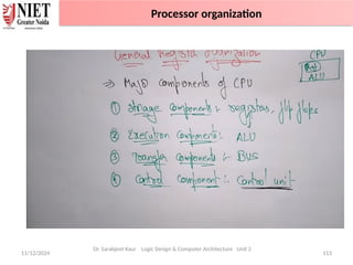
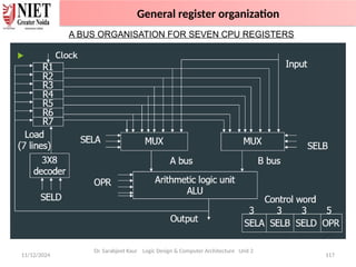
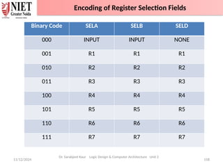
![11/12/2024 109
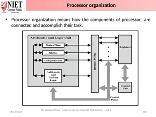
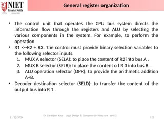
Most computers fall into one of three types of CPU organizations:
• Single accumulator organization.
• General register organization.
• Stack organization.
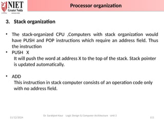
1. Single accumulator organization
• The instruction format in this type of computer uses one address field.
• All operations are performed with an implied accumulator register.
• Example : ADD X
• where X is the address of the operand. The ADD instruction in this case
results in the operation AC <--AC + M[X].
• AC is the accumulator register and M[X] symbolizes the memory word
located at address X.
Dr. Sarabjeet Kaur Logic Design & Computer Architecture Unit 2
Processor organization-General register organization](https://image.slidesharecdn.com/unit2ldcacs-241112135915-7103c9ca/85/Unit_2_LDCA_CS-Computer-Basics-pptx-109-320.jpg)
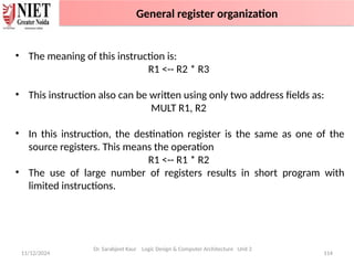
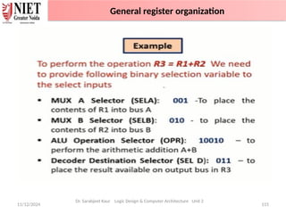
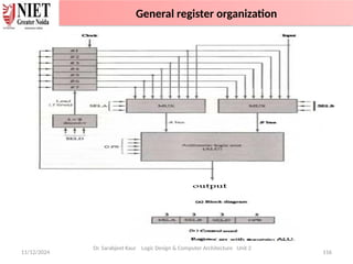
![11/12/2024 110
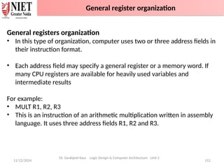
2. General register organization
• The instruction format in this type of computer needs three register
address fields.
• ADD R1, R2, R3 to denote the operation R 1 <---R2 + R3 .
• ADD R1, R2, would denote the operation R 1 <---R1 + R2. Only register
addresses for R 1 and R2 need be specified in this instruction.
• General register-type computers employ two or three address fields in
their instruction format.
• Each address field may specify a processor register or a memory word.
• ADD R1, X
R1 ---- R1 + M [X]
Dr. Sarabjeet Kaur Logic Design & Computer Architecture Unit 2
Processor organization](https://image.slidesharecdn.com/unit2ldcacs-241112135915-7103c9ca/85/Unit_2_LDCA_CS-Computer-Basics-pptx-110-320.jpg)
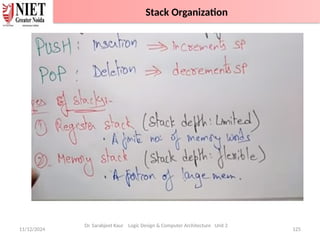
![11/12/2024 Dr. Sarabjeet Kaur Logic Design & Computer Architecture Unit 2 128
PUSH:
• If the stack is not full (FULL =0), a new item is inserted with a push
operation. The push operation consists of the following sequences of
micro operations:
SP ← SP + 1 Increment stack pointer
M [SP] ← DR WRITE ITEM ON TOP OF THE STACK
IF (SP = 0) then (FULL ← 1) Check is stack is full
EMTY ← 0 Mark the stack not empty
Stack Organization](https://image.slidesharecdn.com/unit2ldcacs-241112135915-7103c9ca/85/Unit_2_LDCA_CS-Computer-Basics-pptx-128-320.jpg)
![11/12/2024 Dr. Sarabjeet Kaur Logic Design & Computer Architecture Unit 2 129
POP:
• A new item is deleted from the stack if the stack is not empty (if
EMTY = 0). The pop operation consists of the following sequences of
micro operations:
DR ← M [SP] Read item on top of the stack
SP ← SP - 1 Decrement stack pointer
IF (SP = 0) then (EMTY ← 1) Check if stack is empty
FULL ← 0 Mark the stack not full
• The top item is read from the stack into DR. The stack pointer is
then decremented. If its value reaches zero, the stack is empty, so
EMTY is set to 1.
Stack Organization](https://image.slidesharecdn.com/unit2ldcacs-241112135915-7103c9ca/85/Unit_2_LDCA_CS-Computer-Basics-pptx-129-320.jpg)
![11/12/2024 132
PUSH
• A new item is inserted with the push operation as follows:
SP ← SP - 1
M[SP] ← DR
• The stack pointer is decremented so that it points at the address
of the next word.
• A memory write operation inserts the word from DR into the top
of the stack.
POP
• A new item is deleted with a pop operation as follows:
DR ← M[SP]
SP ← SP + 1
Dr. Sarabjeet Kaur Logic Design & Computer Architecture Unit 2
Stack Organization](https://image.slidesharecdn.com/unit2ldcacs-241112135915-7103c9ca/85/Unit_2_LDCA_CS-Computer-Basics-pptx-132-320.jpg)

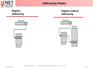
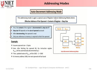
![11/12/2024 140
4. Register Indirect mode:
• In this mode the instruction specifies a register in the CPU whose contents
give the address of the operand in memory.
• The selected register contains the address of the operand rather than the
operand itself.
• MOV AX,[CX] (move the content of memory location addressed by the
register CX to the register AX)
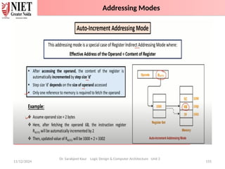
5. Autoincrement/Autodecrement mode:
• This is similar to register indirect mode except that the register is
incremented or decremented after or before its value is used to access
memory.
a) Increment mode- After accessing the operand the contents of this
register are automatically incremented to point to next consecutive
memory location.
Dr. Sarabjeet Kaur Logic Design & Computer Architecture Unit 2
Addressing Modes](https://image.slidesharecdn.com/unit2ldcacs-241112135915-7103c9ca/85/Unit_2_LDCA_CS-Computer-Basics-pptx-140-320.jpg)
![11/12/2024 141
Example: Add R1, (R2+)
OR
R1 = R1 + M[R2]
R2 = R2 + d
Useful for stepping through arrays in a loop.
R2 – start of the array, d- size of an element.
b) Decrement Mode:
• Before accessing the operand , the contents of this register are
automatically decremented to point to the previous consecutive memory
location.
Example- Add R1, (-R2)
OR
R2 = R2 – d
R1 = R1 + M [R2]
Dr. Sarabjeet Kaur Logic Design & Computer Architecture Unit 2
Addressing Modes](https://image.slidesharecdn.com/unit2ldcacs-241112135915-7103c9ca/85/Unit_2_LDCA_CS-Computer-Basics-pptx-141-320.jpg)
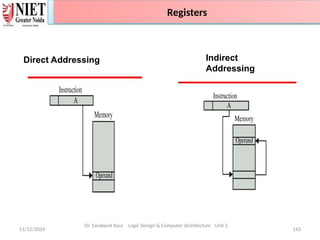
![11/12/2024 142
6. Direct Address mode:
• In this mode the effective address is equal to the address part of the
instruction.
• The operand resides in memory and its address is given directly by the
address field of the instruction.
• Example – ADD AL, [0301] (add the content of address 0301 to A)
7. Indirect Address mode :
• In this mode the address field of the instruction gives the address where
the effective address is stored in memory.
• In this address field of instruction gives the address where the effective
address is stored in memory.
Dr. Sarabjeet Kaur Logic Design & Computer Architecture Unit 2
Addressing Modes](https://image.slidesharecdn.com/unit2ldcacs-241112135915-7103c9ca/85/Unit_2_LDCA_CS-Computer-Basics-pptx-142-320.jpg)
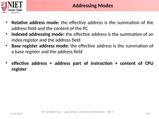


![COA_UNIT-1new[1].pdf](https://cdn.slidesharecdn.com/ss_thumbnails/coaunit-1new1-230919072310-a464b1d1-thumbnail.jpg?width=640&height=640&fit=bounds)


