The document introduces a new platform, einscg+, designed for rapid clock and memory activity takedown in high-performance microprocessor designs, combining logic verification, debug, and RTL analysis. It highlights the platform's ability to quickly identify power-saving opportunities and improve design efficiency, achieving results in approximately three minutes. The paper also discusses various use-cases demonstrating the platform's effectiveness and emphasizes its generic applicability for future designs.
![ Over the last decade or so, several techniques were proposed for enabling RTL analysis. But with the
advent of FinFET based designs [1], there is renewed focus on dynamic power analysis and mitigation [2],
especially early in the design flow [3] using techniques like clock gating [4] and memory activity takedown.
Additionally, high performance microprocessor design blocks are getting larger, with increasing number of
clock gating domains and with notable differences in activity across these domains and workloads [5].
The turn around time for performing RTL analysis using quick synthesis followed by netlist based tool
engines [6,7,8] is not efficient for rapid clock and memory activity exploration. Formal techniques [9,10],
though comprehensive, do not accurately capture the dependency of clock and memory activity on the
workloads.
Techniques in [3], for early activity analysis, require development of dedicated software for test-bench
creation and activity analysis. Also, even though thorough analysis is presented in a graphically rich
manner, further debug and activity reduction of highly active blocks is non-intuitive to the designer.
In this paper, we present a new platform for enabling rapid clock and memory activity takedown and its
application for design of a next generation industry class high performance microprocessor [1]. To the
best of our knowledge, this is the first such platform which brings together principles of designer level logic
verification, logic debug and light-weight netlist creation, while specifically catering to the requirements of
rapid RTL activity takedown.
Slide 2
Motivation](https://image.slidesharecdn.com/einscgdac2017-171117151807/75/Techniques-for-Efficient-RTL-Clock-and-Memory-Gating-Takedown-of-Next-Generation-High-performance-Microprocessor-Designs-2-2048.jpg)
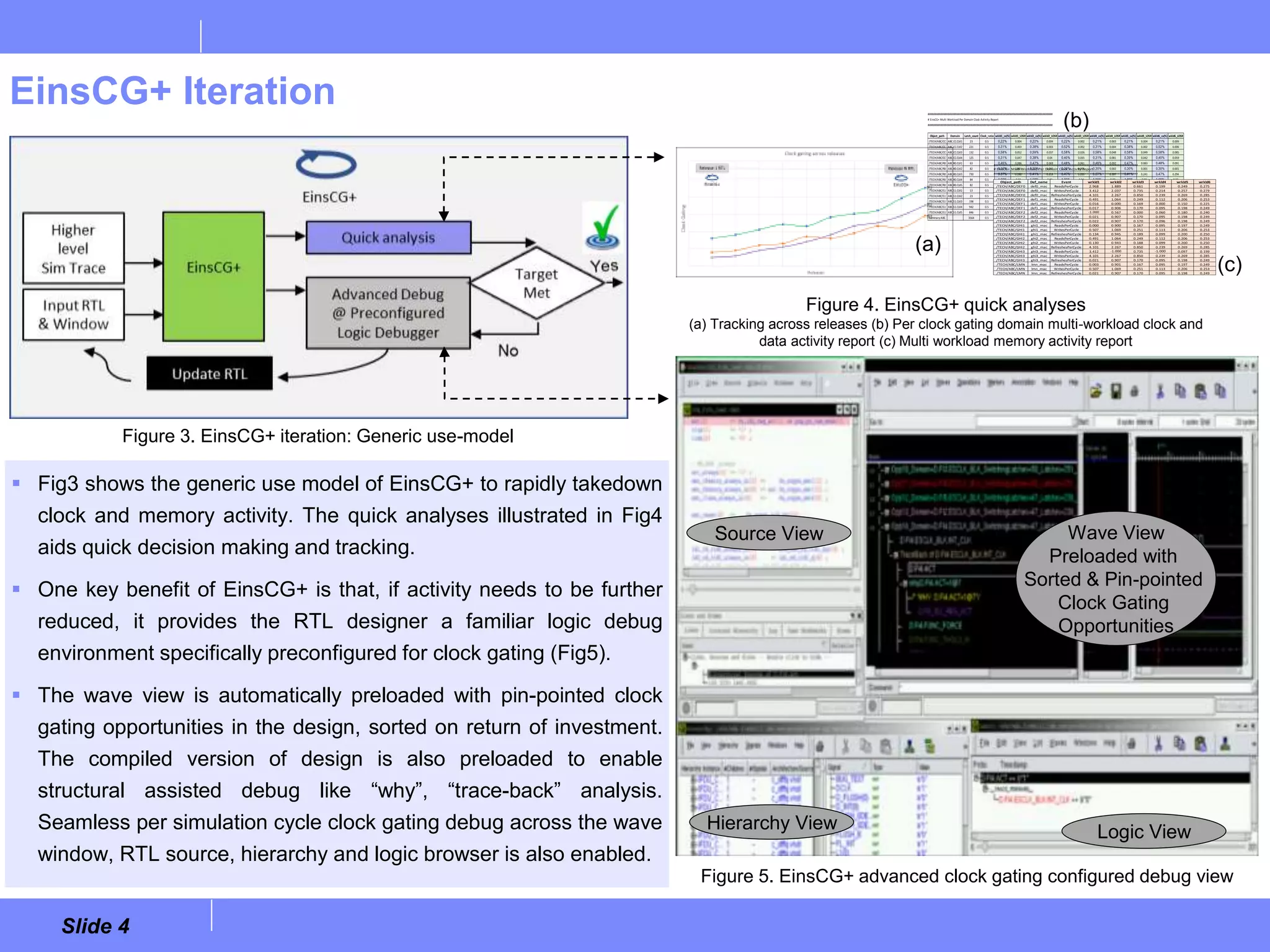
![Slide 3
Main Idea
Bring together principles of designer level logic
verification trace import and simulation replay [11],
logic debug [12, 14] and virtual logic netlist based
RTL analysis [13], to specifically cater to the
requirements of rapid RTL activity takedown.
Fig1 shows key EDA building blocks for building the
platform and Fig2 shows how these were “tied
together” to create the EinsCG+ platform for
enabling rapid clock and memory activity takedown.
(Details in foot notes)
Figure 1. Clock & memory gating platform
– pieces of the puzzle
Figure 2. EinsCG+ software architecture
Enables logic designers with a pre-configured (yet
familiar) platform for meeting clock and memory
gating targets.
Enables rapid exploration of power saving
opportunities across IP blocks, use-scenarios,
workloads and workload windows. (Input block RTL to
next set of pin-pointed opportunities in ~3 minutes)
Low platform development cost (~1 month). Except
building block 9, rest are available in modern day
industry class EDA-suites like [14].
Key Idea Key Benefits](https://image.slidesharecdn.com/einscgdac2017-171117151807/75/Techniques-for-Efficient-RTL-Clock-and-Memory-Gating-Takedown-of-Next-Generation-High-performance-Microprocessor-Designs-3-2048.jpg)
![ Use-case1: EinsCG+ helped identify sub-design blocks of a design under test (DUT) not meeting clock and/or memory gating
criteria and independently iterate on those blocks to close on targets, before redoing the analysis on DUT. Capability of
EinsCG+ to perform on-the-fly re-simulation from an existing DUT trace, eliminated the need for higher level DUT analysis for
individual RTL update iteration, while allowing for evaluation of individual block level updates for clock gating by different
designers in parallel.
Use-case2: Use of vendor IP in microprocessor designs is becoming increasingly common in the era of Open Compute [15].
Such IP blocks are often used in different modes across the design. While the vendor IP blocks may be designed efficiently for
power, incorrect mode configuration can result in high activity and power. Independent EinsCG+ iterative analysis on specific
vendor IP instances in the design enabled ensuring the correct mode configuration.
Use-case3: EinsCG+ analysis on the design was used to identify activity peaks and corresponding simulation windows. To
takedown these activity peaks, EinsCG+ was used iteratively on simulation windows of interest, especially for larger workloads.
Slide 5
Experimental Evaluation
Figure 7. Use-case2
Vendor IP mode configuration
Figure 6. Use-case1
EinsCG+ iterations on sub-designs
Figure 8. Use-case3
EinsCG+ workload analysis](https://image.slidesharecdn.com/einscgdac2017-171117151807/75/Techniques-for-Efficient-RTL-Clock-and-Memory-Gating-Takedown-of-Next-Generation-High-performance-Microprocessor-Designs-5-2048.jpg)


![[IJET-V1I3P5] Authors :Dushyant Kumar Soni, Ashish Hiradhar](https://cdn.slidesharecdn.com/ss_thumbnails/ijet-v1i3p5-150519153226-lva1-app6891-thumbnail.jpg?width=640&height=640&fit=bounds)