Download as PDF, PPTX

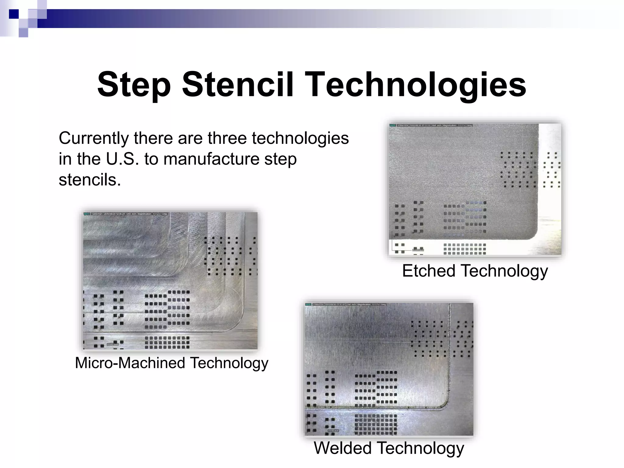
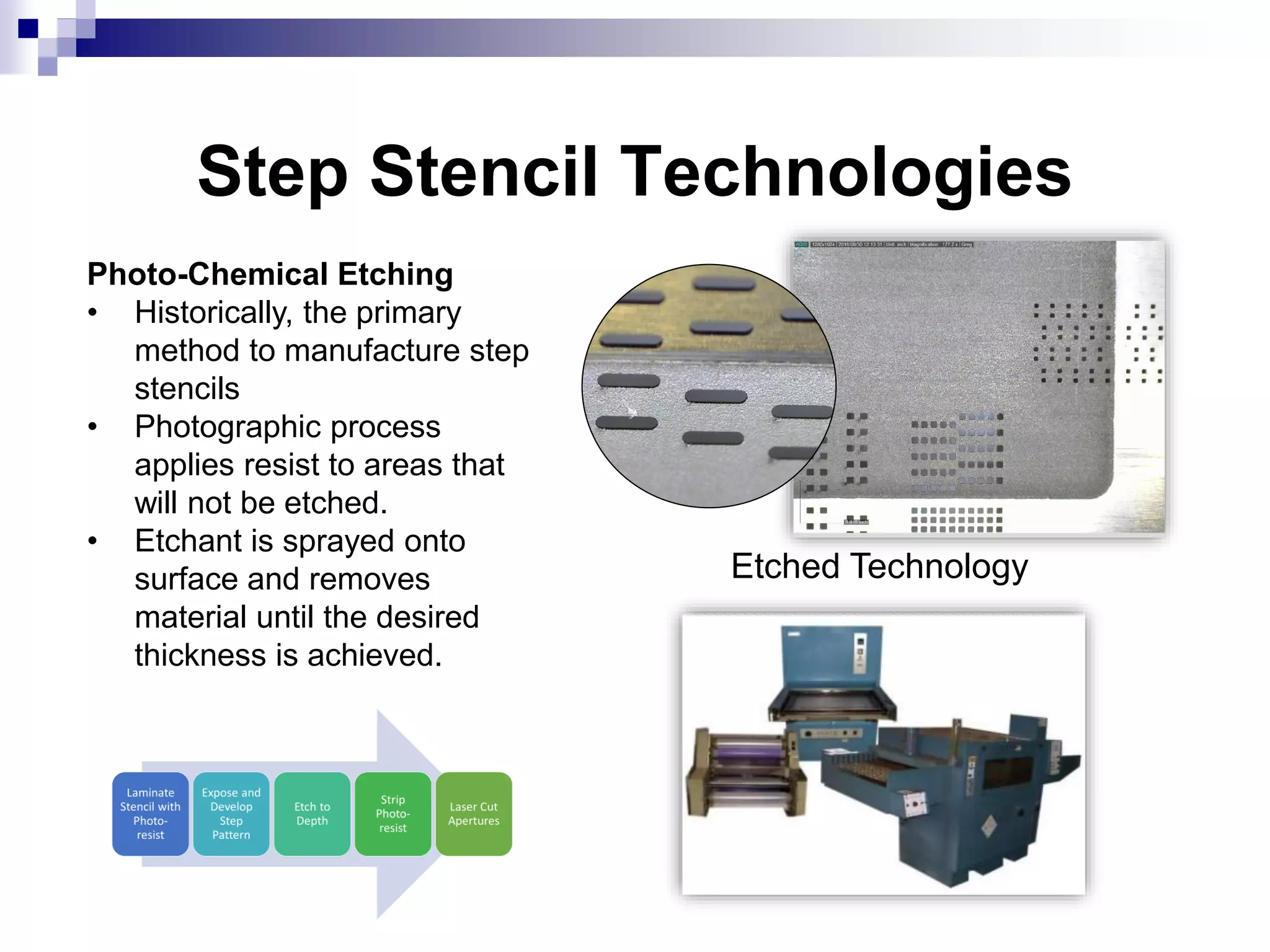
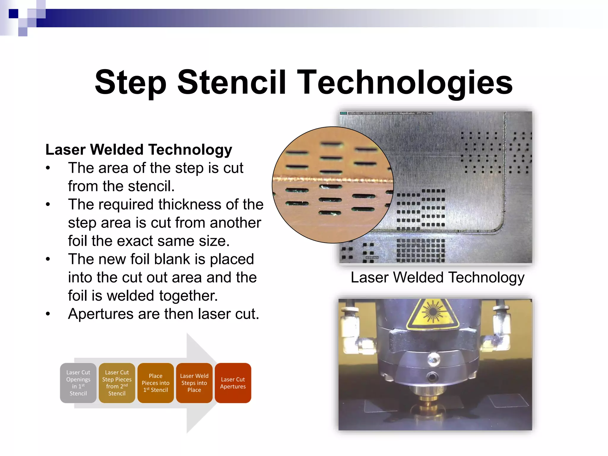
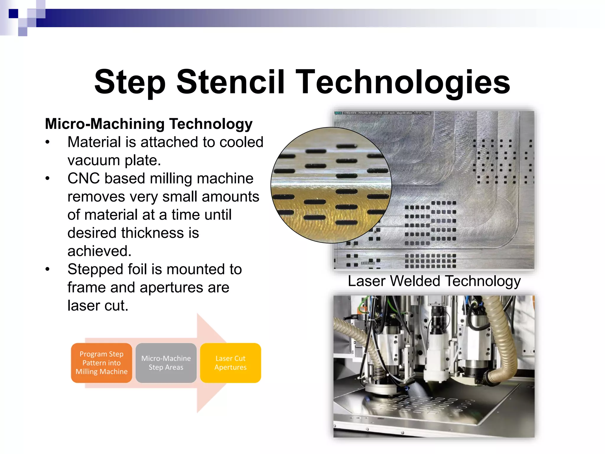
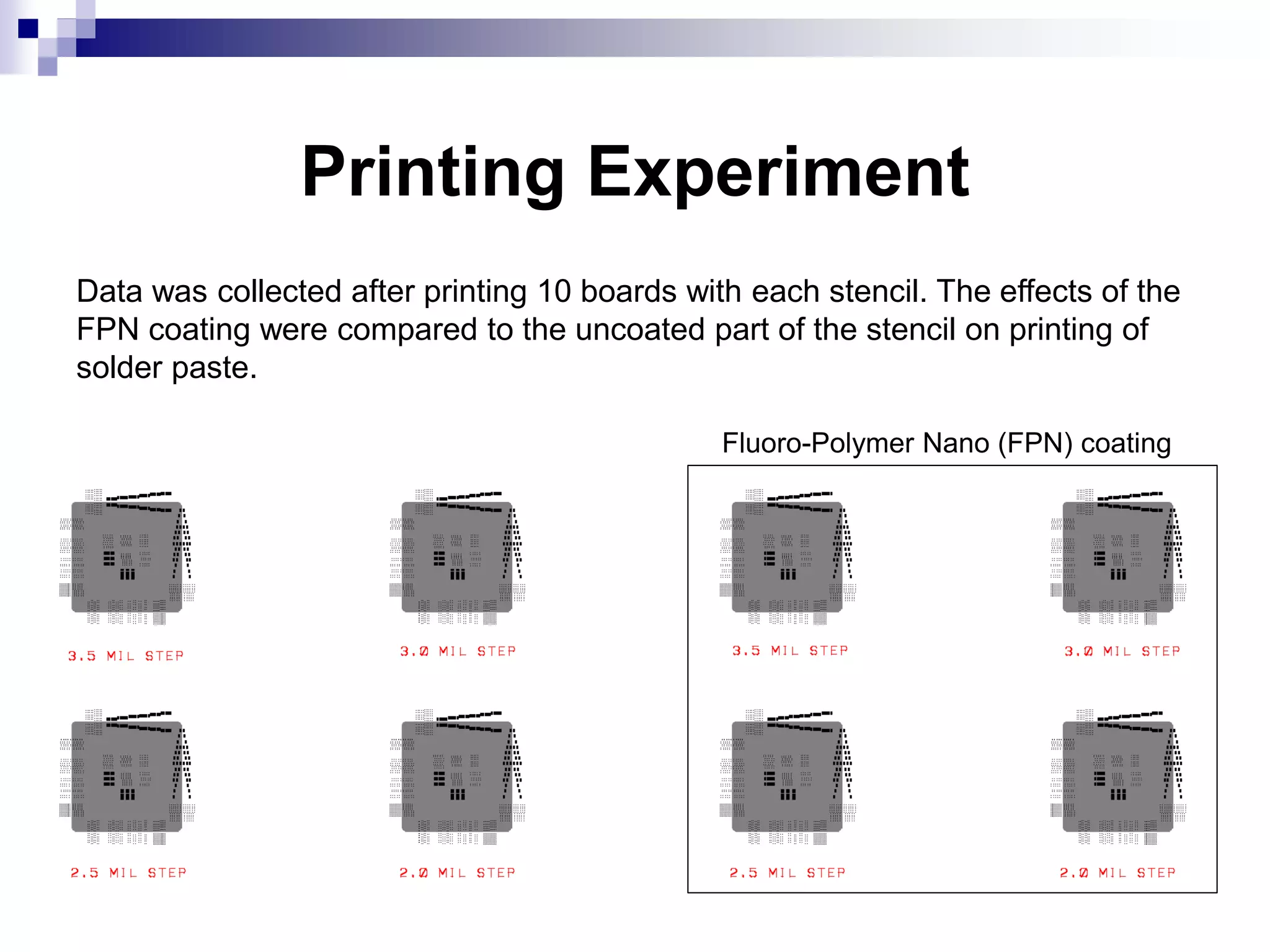
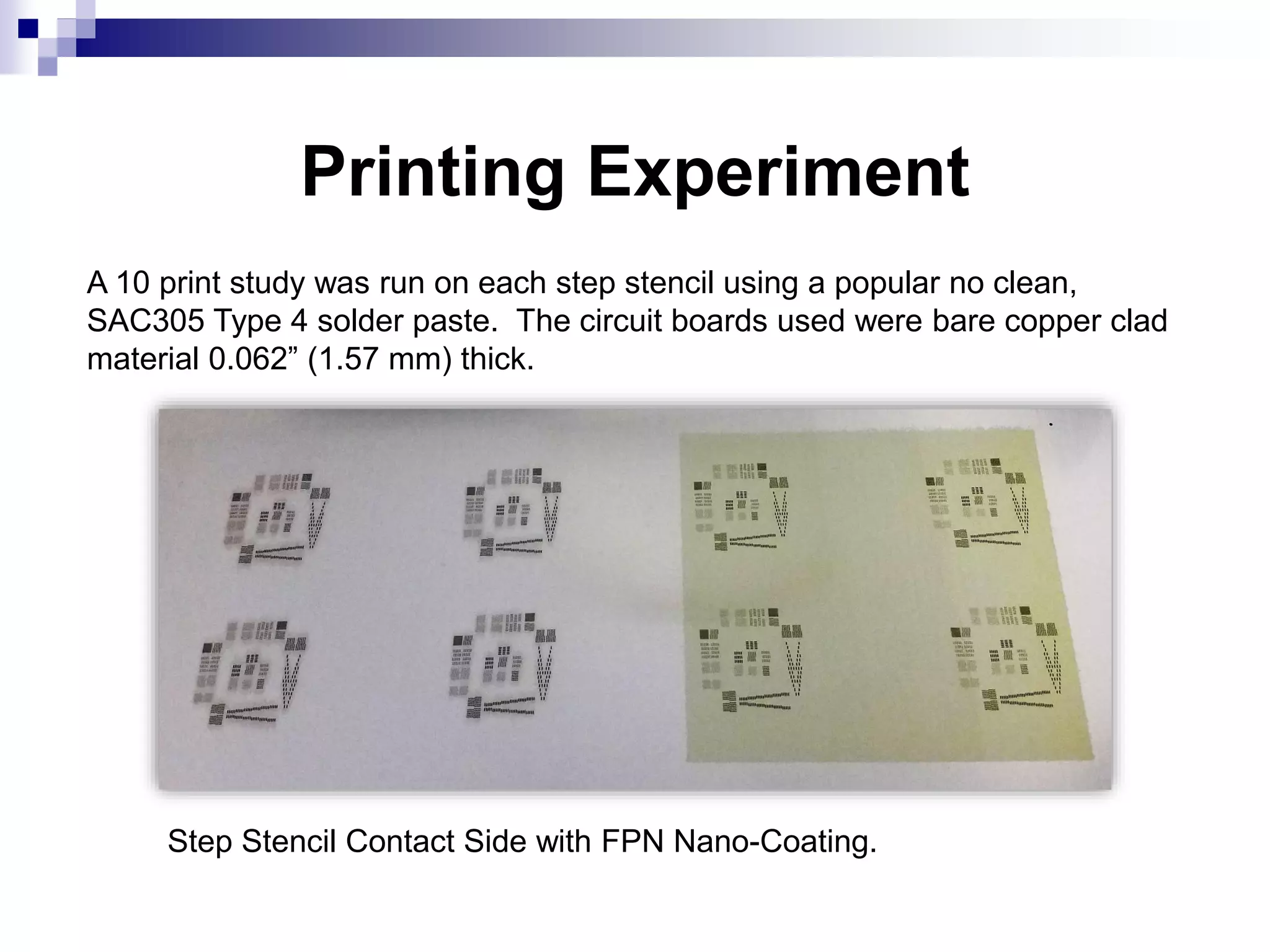
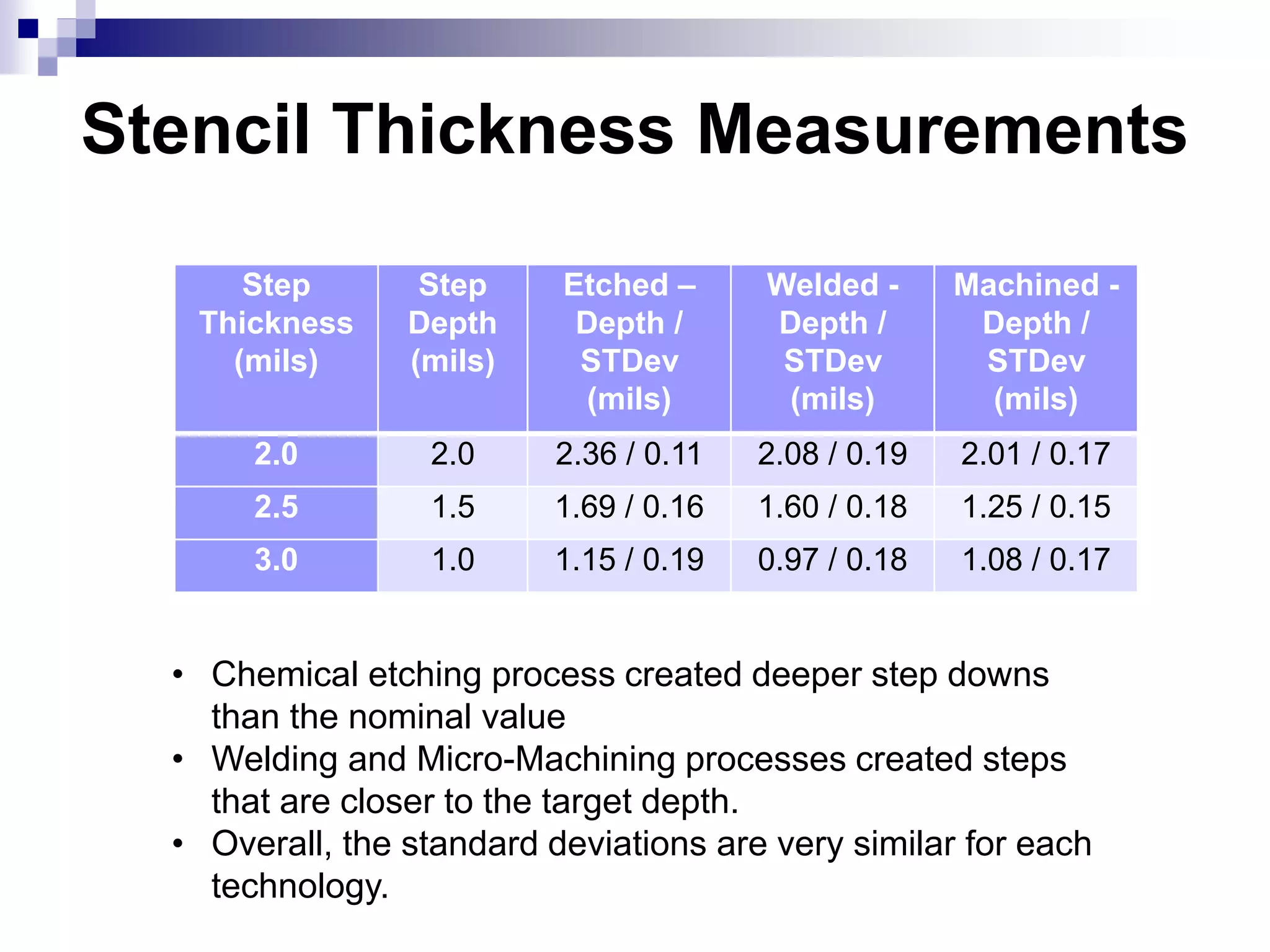
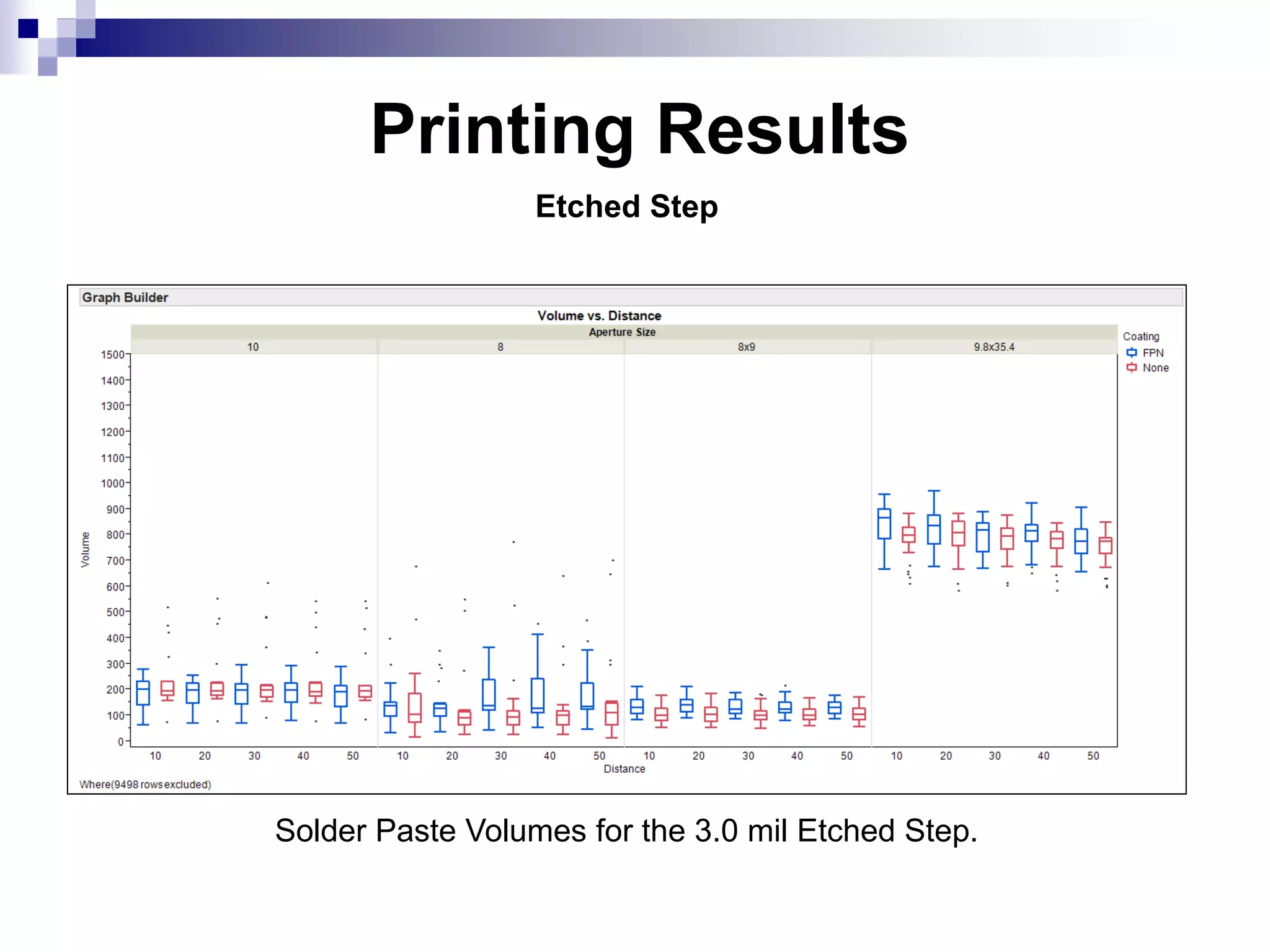
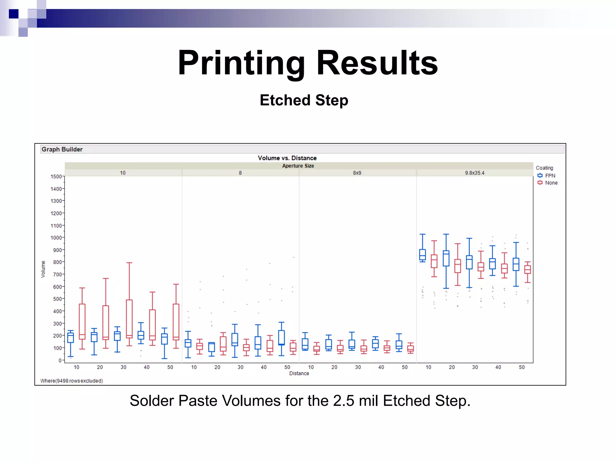
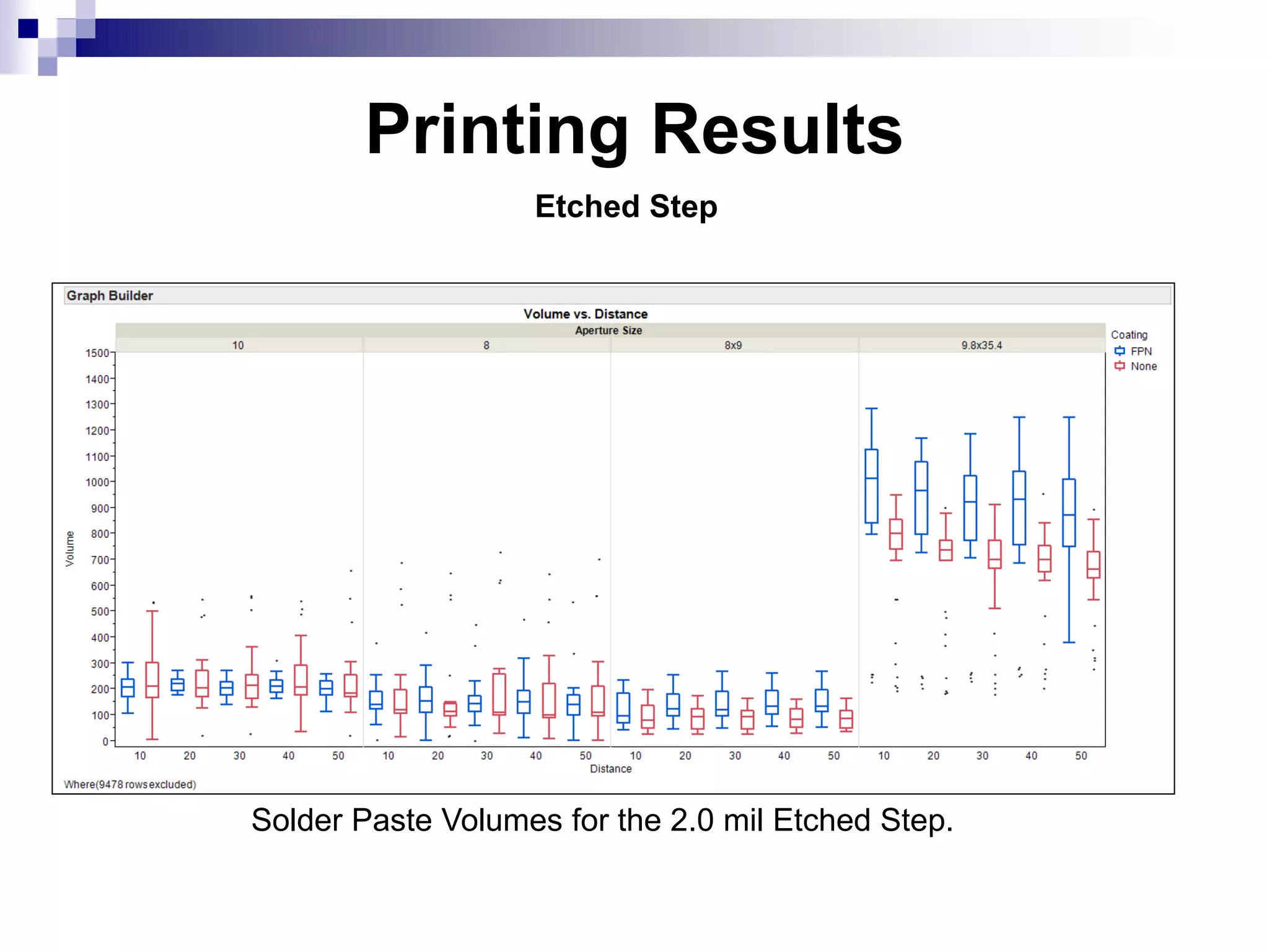

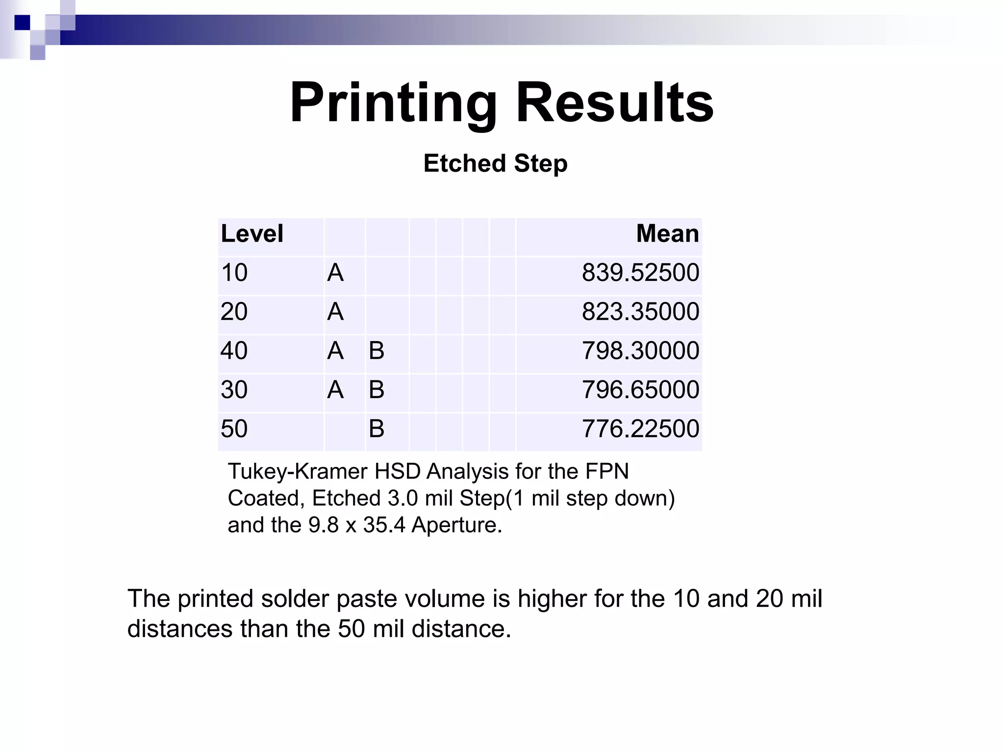

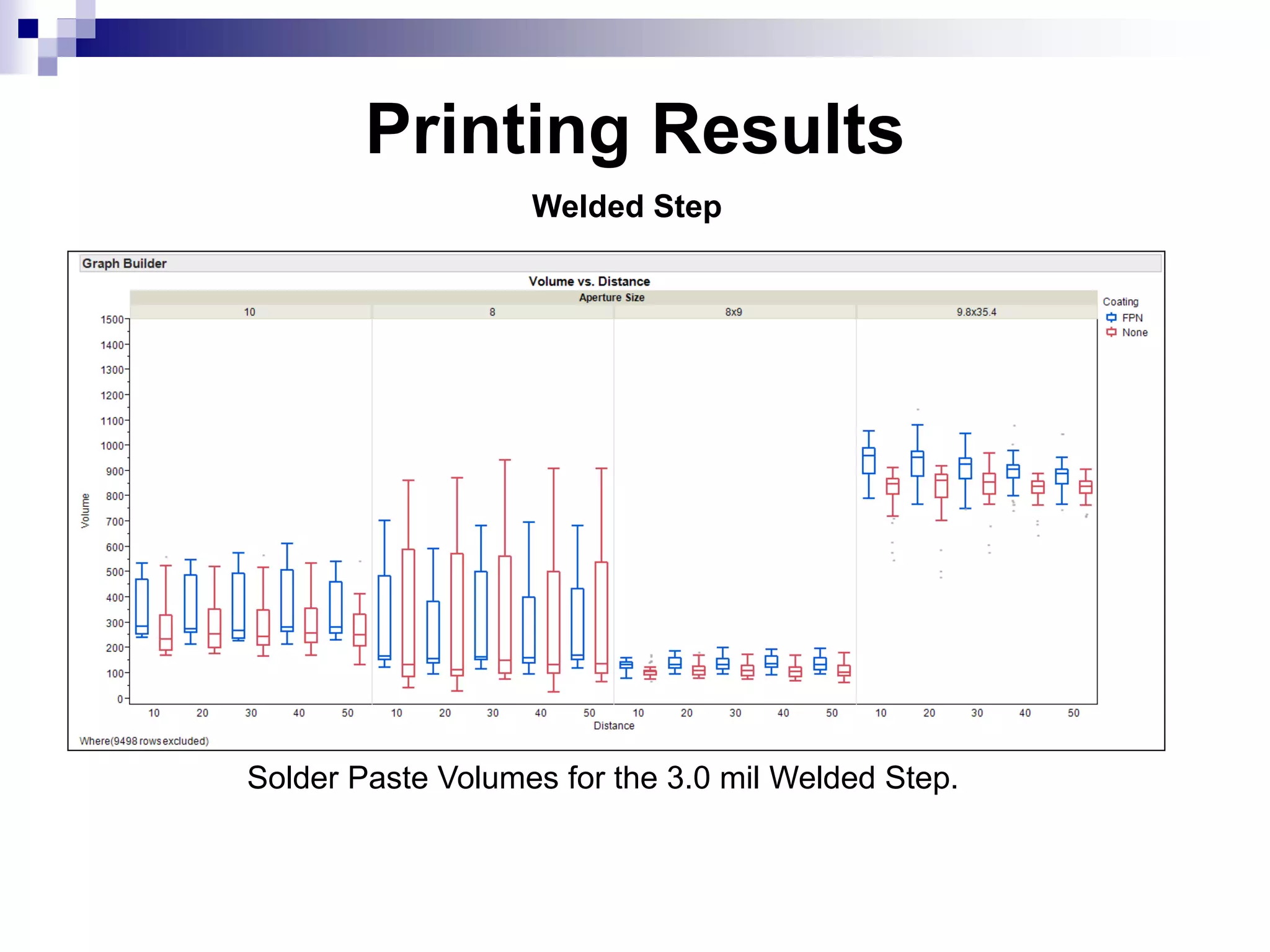

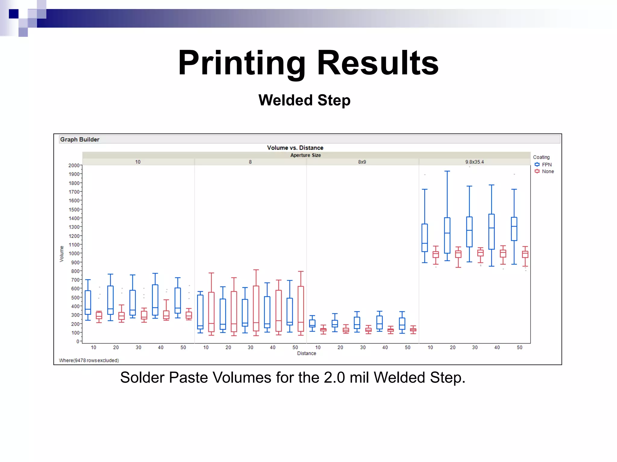

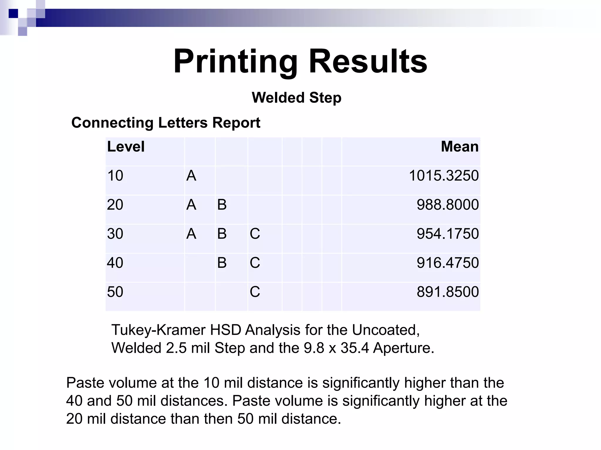
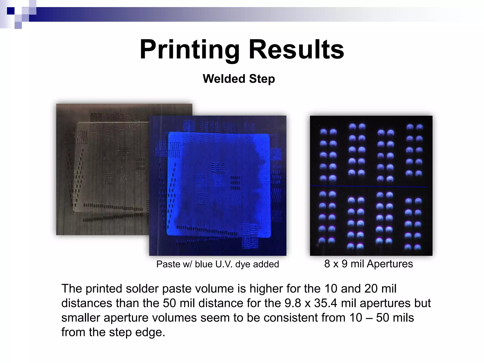

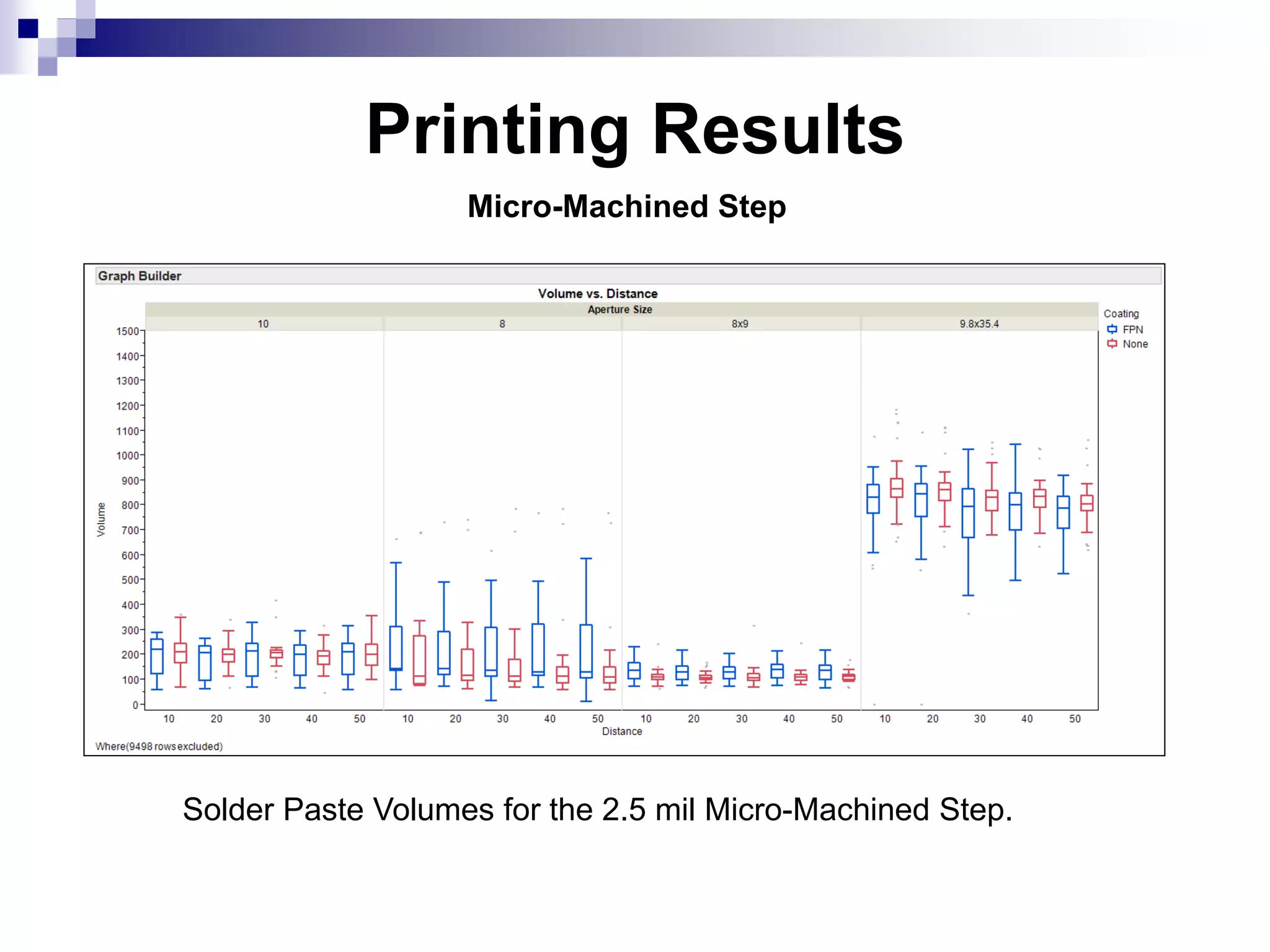

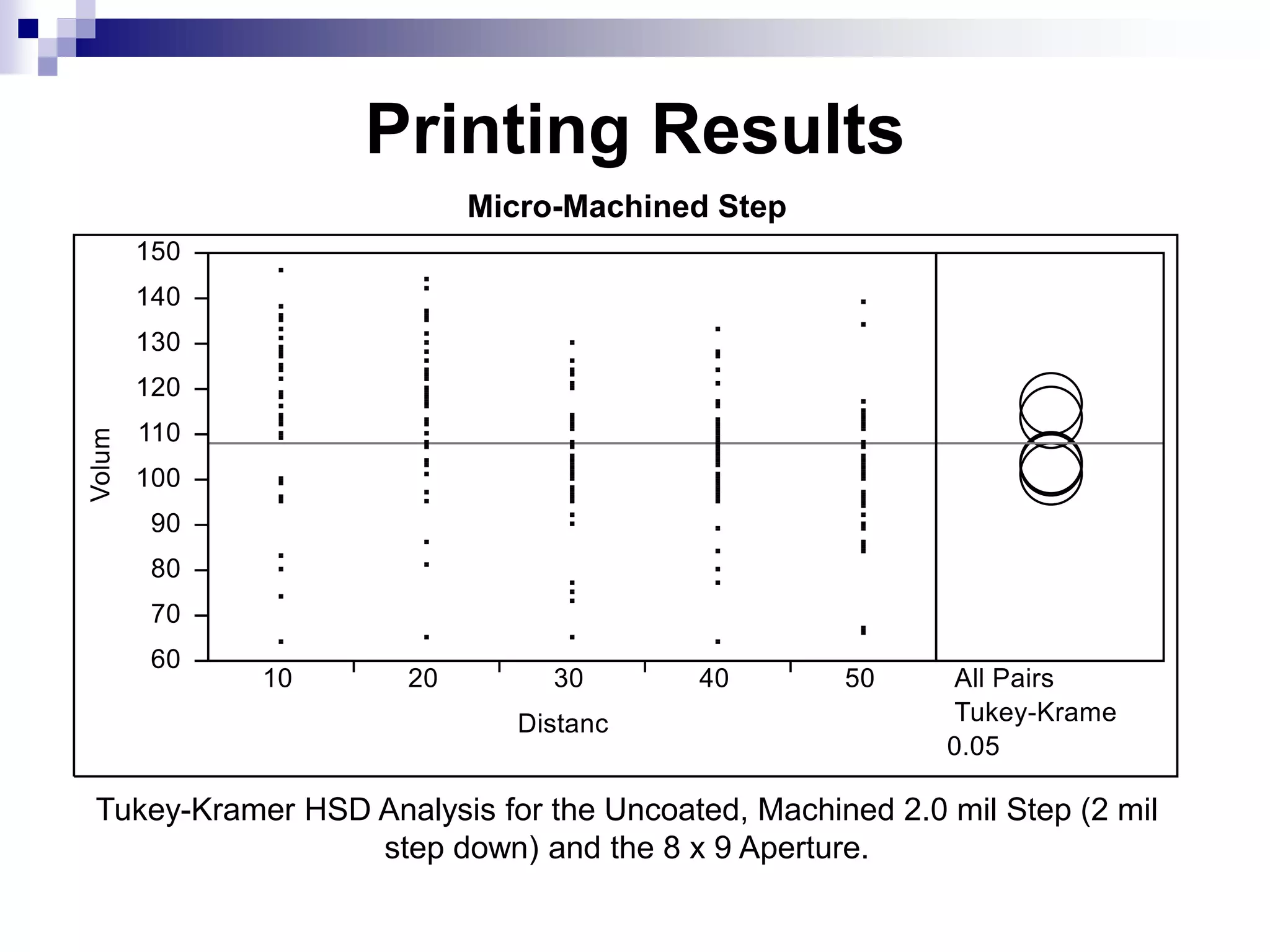
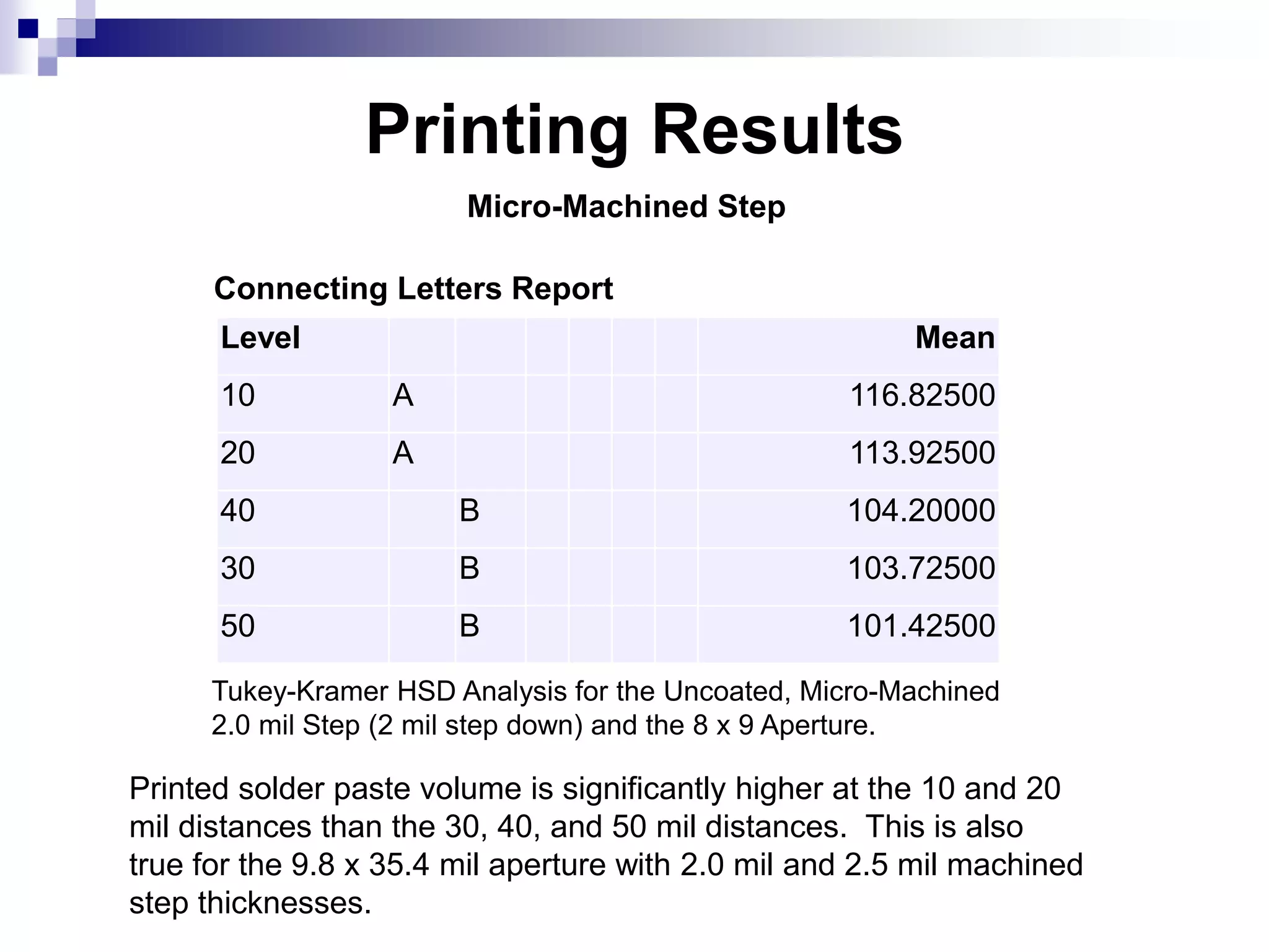
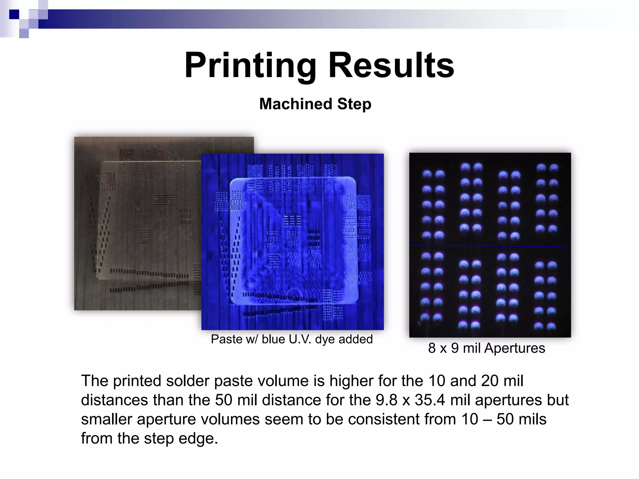


The document outlines the technology and applications of step stencils in solder paste printing, discussing the different manufacturing methods including chemical etching, laser welding, and micro-machining. Experimental results indicate that solder paste volume is optimized when applied 10-20 mils away from the step edge, and that the FPN coating improves paste volume consistency. Future work includes further investigations into paste volume distribution and performance comparisons with non-stepped stencils.


