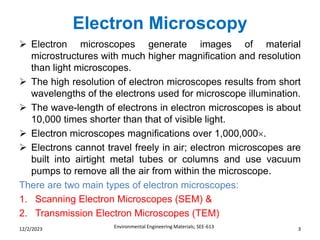
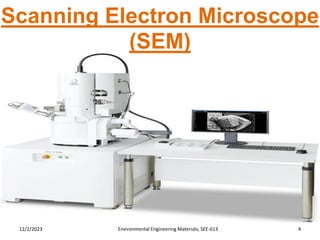
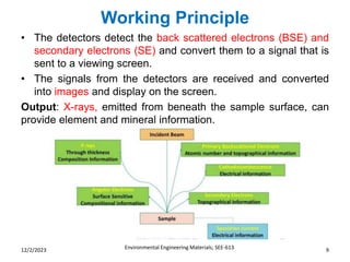
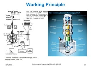
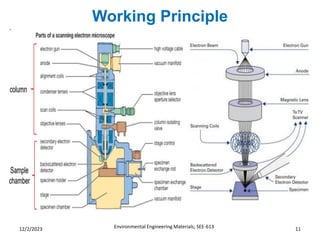
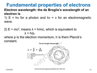
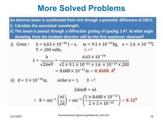
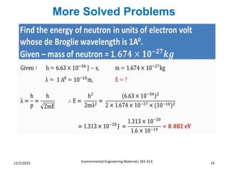
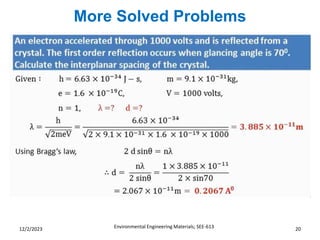
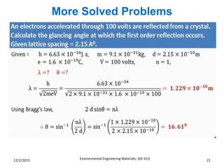
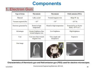
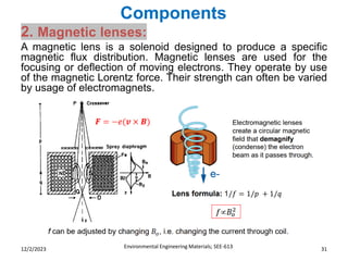
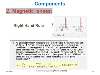
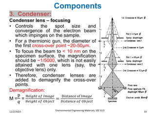
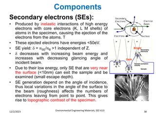
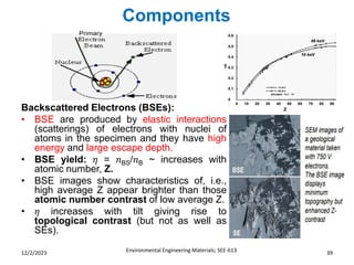
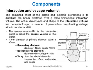
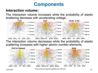
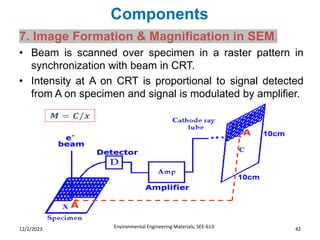
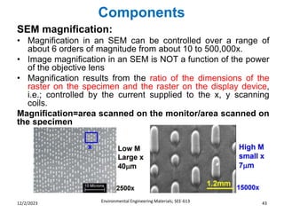
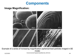
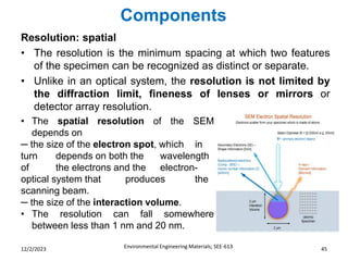
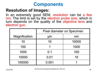
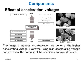
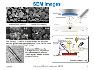
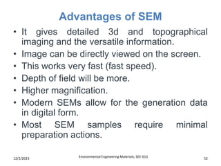
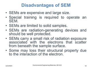
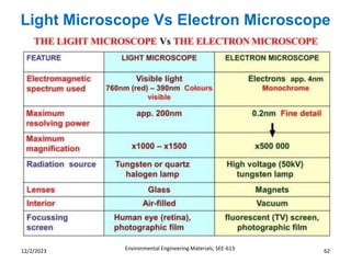
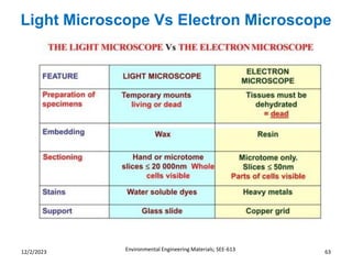
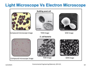
Scanning Electron Microscopes (SEM) & Transmission Electron Microscopes (TEM)
1. Undergraduate Course
Environmental Engineering Materials
(SEE-613) Theory
Course Instructor:
Engr. Shahbaz Hussain
Department of Structures and Environmental Engineering
University of Agriculture, Faisalabad-Pakistan
3. Electron Microscopy
Environmental Engineering Materials; SEE-613 3
12/2/2023
➢ Electron microscopes generate images of material
microstructures with much higher magnification and resolution
than light microscopes.
➢ The high resolution of electron microscopes results from short
wavelengths of the electrons used for microscope illumination.
➢ The wave-length of electrons in electron microscopes is about
10,000 times shorter than that of visible light.
➢ Electron microscopes magnifications over 1,000,000.
➢ Electrons cannot travel freely in air; electron microscopes are
built into airtight metal tubes or columns and use vacuum
pumps to remove all the air from within the microscope.
There are two main types of electron microscopes:
1. Scanning Electron Microscopes (SEM) &
2. Transmission Electron Microscopes (TEM)
5. Introduction
Environmental Engineering Materials; SEE-613 5
12/2/2023
Def: A Scanning Electron Microscope (SEM) is a type of electron
microscope that images a sample by scanning it with a high energy
beam of electrons in a raster scan pattern.
• The electrons interact with the atoms that make up the sample
producing signals that contain information about the sample:
➢ Surface topography: The surface features Of an Object or "how it looks", its
texture; direct relation between features and materials properties.
➢ Morphology: The shape and size Of the particles making up the Object; direct
relation between the structures and materials properties.
➢ Composition: The elements and compounds that the object is composed of and
the relative amounts of them; direct relationship between composition and
materials properties
➢ Crystallographic Information: HOW the atoms are arranged in the Object; direct
relation between these arrangements and material properties.
➢ and other properties such as electrical conductivity.
• Scanning electron microscopy is used for inspecting
topographies of specimens at very high magnifications using a
piece of equipment called the scanning electron microscope.
6. Introduction
Environmental Engineering Materials; SEE-613 6
12/2/2023
• SEM magnifications can go to
more than 300,000 X but most
semiconductor manufacturing
applications require
magnifications of less than
3,000 X only.
• Resolution of objects of nearly
1 nm.
• Specimens can be observed in
high vacuum, low vacuum and
in Environmental SEM
specimens can be observed in
wet condition.
• Gives 3D views of the exteriors
of the objects like cells,
microbes or surfaces.
8. Working Principle
Environmental Engineering Materials; SEE-613 8
12/2/2023
• The basic principle is that a beam of electrons is generated by
a suitable source, typically a tungsten filament (W) cathode or
a field emission gun and passed towards the anode.
• The electron beam, is accelerated through a high voltage
ranging from 0.2 keV to 40 keV and pass through a system of
apertures in a vertical path through the column of the
microscope in a concentrated manner and electromagnetic
lenses to produce a thin beam of electrons, is focused by one
or two condenser lenses to a spot about 0.4 nm to 5 nm in
diameter.
• Then the beam passes through pairs of scanning coils or
pairs of deflector plates in the electron column, which deflects
the beam in the X and Y axis so that it scans in a raster
fashion (rectangular area) of the sample surface.
• Then the beam scans the surface of the specimen, electrons
are emitted from the specimen by the action of the scanning
beam and collected by a suitably positioned detector.
9. Working Principle
Environmental Engineering Materials; SEE-613 9
12/2/2023
• The detectors detect the back scattered electrons (BSE) and
secondary electrons (SE) and convert them to a signal that is
sent to a viewing screen.
• The signals from the detectors are received and converted
into images and display on the screen.
Output: X-rays, emitted from beneath the sample surface, can
provide element and mineral information.
13. Fundamental properties of electrons
Environmental Engineering Materials; SEE-613 13
12/2/2023
Electron wavelength: the de Broglie’s wavelength of an
electron is
1) E = hν for a photon and λν = c for an electromagnetic
wave.
2) E = mc2, means λ = h/mc, which is equivalent to
λ = h/p.
where p is the electron momentum, h is them Planck’s
constant.
14. Fundamental properties of electrons
Environmental Engineering Materials; SEE-613 14
12/2/2023
de- Broglie wavelength of an electron
Let us consider an electron of mass m and charge e.
v = final velocity attained by electron when it is accelerated from rest through
a potential difference of V volts
kinetic energy = work done on electron by electric field
15. Unsolved Problems
Environmental Engineering Materials; SEE-613 15
12/2/2023
Question 1: An electron and a photon have the same
wavelength. If p is the momentum of the electron and E is
the energy of the photon, the magnitude of p/E in SI unit
is
(a) 3.0 108 (b) 3.33 10-9
(c) 9.1 10-31 (d) 6.64 10-34
Question 2: What is the wavelength of an electron moving
at 5.31 x 10⁶ m/sec?
Given: mass of electron = 9.11 x 10⁻³¹ kg h = 6.626 x 10⁻³⁴ J·s
16. Solved Problems
Environmental Engineering Materials; SEE-613 16
12/2/2023
Question 1: An electron and a photon have the same
wavelength. If p is the momentum of the electron and E is
the energy of the photon, the magnitude of p/E in SI unit
is
(a) 3.0 108 (b) 3.33 10-9
(c) 9.1 10-31 (d) 6.64 10-34
As we know, for an electron, λ = h/p
Or
p = h/λ
And for photon E = hc / λ
Thus, p / E = 1 / c = 1 / (3 x 10⁸ m/s) = 0. 33 x 10-8 s/m
17. Solved Problems
Environmental Engineering Materials; SEE-613 17
12/2/2023
Question 2: What is the wavelength of an electron
moving at 5.31 x 10⁶ m/sec?
Given: mass of electron = 9.11 x 10⁻³¹ kg h = 6.626 x 10⁻³⁴ J·s
de Broglie’s equation is
λ = h/mv
λ = 6.626 x 10⁻³⁴ J·s/ 9.11 x 10-31 kg x 5.31 x 106 m/sec
λ = 6.626 x 10⁻³⁴ J·s/4.84 x 10-24 kg·m/sec
λ = 1.37 x 10⁻¹⁰ m
λ = 1.37 Å
The wavelength of an electron moving 5.31 x 10⁶ m/sec is
1.37 x 10⁻¹⁰ m or 1.37 Å.
27. SEM Overview
Environmental Engineering Materials; SEE-613 27
12/2/2023
Electrons can interact with matter generating numerous signals in different pathways
28. Components
Environmental Engineering Materials; SEE-613 28
12/2/2023
1. Electron gun consisting of cathode and anode
2. The condenser lens controls the amount of
electrons travelling down the column.
3. The objective lens focuses the beam into a spot
on the sample.
4. Deflection coil helps to deflect the electron beam.
5. X-Y scan coils & scan generator.
6. Backscatter Electron Detector (BED)
7. Secondary Electron Detector (SED) attracts the
secondary electrons.
8. Additional sensors detect backscattered
electrons and x-rays.
9. Sample stage.
10.Computer and display to view the images.
11.External vacuum pump(s).
31. Components
Environmental Engineering Materials; SEE-613 31
12/2/2023
2. Magnetic lenses:
A magnetic lens is a solenoid designed to produce a specific
magnetic flux distribution. Magnetic lenses are used for the
focusing or deflection of moving electrons. They operate by use
of the magnetic Lorentz force. Their strength can often be varied
by usage of electromagnets.
33. Components
Environmental Engineering Materials; SEE-613 33
12/2/2023
3. Condenser:
Condenser lens – focusing
• Controls the spot size and
convergence of the electron beam
which impinges on the sample.
• For a thermionic gun, the diameter of
the first cross-over point ~20-50µm.
• To focus the beam to < 10 nm on the
specimen surface, the magnification
should be ~1/5000, which is not easily
attained with one lens (say, the
objective lens) only.
• Therefore, condenser lenses are
added to demagnify the cross-over
points.
Demagnification:
M =
p
𝑞
=
Hei𝑔ℎ𝑡 𝑜𝑓 𝐼𝑚𝑎𝑔𝑒
𝐻𝑒𝑖𝑔ℎ𝑡 𝑜𝑓 𝑂𝑏𝑗𝑒𝑐𝑡
=
Distance of I𝑚𝑎𝑔𝑒
𝐷𝑖𝑠𝑡𝑎𝑛𝑐𝑒 𝑜𝑓 𝑂𝑏𝑗𝑒𝑐𝑡
34. Components
Environmental Engineering Materials; SEE-613 34
12/2/2023
4. Objective:
Objective lens – final probe forming
• Controls the final focus of the electron
beam by changing the magnetic field
strength
• Since the electrons coming from the
electron gun have spread in kinetic
energies and directions of movement,
they may not be focused to the same
plane to form a sharp spot.
• By inserting an aperture, the stray
electrons are blocked, and the
remaining narrow beam will come to a
narrow
• The cross -over image is finally
demagnified to an ~10nm beam spot
which carries a beam current of
approximately 10-9 – 10-12 Å.
35. Components
Environmental Engineering Materials; SEE-613 35
12/2/2023
5. Scanning coils:
Scanning coils in a SEM are used to raster
the beam across the sample for textural
imaging.
• Two sets of coils are used for scanning
the electron beam across the specimen
surface in a raster fashion over a
rectangular area of the sample surface.
• This effectively samples the specimen
surface point by point over the scanned
area.
37. Components
Environmental Engineering Materials; SEE-613 37
12/2/2023
• The types of signals produced by a SEM include
secondary electrons (SEs), back-scattered
electrons (BSEs), characteristic X-rays and photons
(cathodoluminescence) (CL), absorbed current
(specimen current) and transmitted electrons. Both
SEs and BSEs are used for imaging
38. Components
Environmental Engineering Materials; SEE-613 38
12/2/2023
Secondary electrons (SEs):
• Produced by inelastic interactions of high energy
electrons with core electrons (K, L M shells) of
atoms in the specimen, causing the ejection of the
electrons from the atoms. T
• These ejected electrons have energies <50eV.
• SE yield: = 𝑛SE/𝑛B >1 independent of Z.
• decreases with increasing beam energy and
increases with decreasing glancing angle of
incident beam.
• Due to their low energy, only SE that are very near
the surface (<10nm) can exit the sample and be
examined (small escape depth).
• SE generation depend on the angle of incidence,
thus local variations in the angle of the surface to
the beam (roughness) affects the numbers of
electrons leaving from point to point. This gives
rise to topographic contrast of the specimen.
39. Components
Environmental Engineering Materials; SEE-613 39
12/2/2023
Backscattered Electrons (BSEs):
• BSE are produced by elastic interactions
(scatterings) of electrons with nuclei of
atoms in the specimen and they have high
energy and large escape depth.
• BSE yield: 𝜂 = 𝑛BS/𝑛B ~ increases with
atomic number, Z.
• BSE images show characteristics of, i.e.,
high average Z appear brighter than those
atomic number contrast of low average Z.
• 𝜂 increases with tilt giving rise to
topological contrast (but not as well as
SEs).
40. Components
Environmental Engineering Materials; SEE-613 40
12/2/2023
Interaction and escape volume:
The combined effect of the elastic and inelastic interactions is to
distribute the beam electrons over a three-dimensional interaction
volume. The actual dimensions and shape of the interaction volume
are dependent upon a number of parameters: accelerating voltage,
atomic number and tilt.
• The volume responsible for the respective
signal is called the escape volume of that
signal.
• If the diameter of primary electron beam is
~5nm:
─ Secondary electron:
diameter~10nm; depth~10nm
─ Backscattered electron:
diameter~1mm; depth~1mm
─ X-ray: from the whole interaction
volume, i.e., ~5mm in diameter
and depth
41. Components
Environmental Engineering Materials; SEE-613 41
12/2/2023
Interaction volume:
The interaction volume increases while the probability of elastic
scattering decrease with accelerating voltage.
The interaction volume decreases while the probability of elastic
scattering increases with higher atomic number elements.
42. Components
Environmental Engineering Materials; SEE-613 42
12/2/2023
7. Image Formation & Magnification in SEM.
• Beam is scanned over specimen in a raster pattern in
synchronization with beam in CRT.
• Intensity at A on CRT is proportional to signal detected
from A on specimen and signal is modulated by amplifier.
43. Components
Environmental Engineering Materials; SEE-613 43
12/2/2023
SEM magnification:
• Magnification in an SEM can be controlled over a range of
about 6 orders of magnitude from about 10 to 500,000x.
• Image magnification in an SEM is NOT a function of the power
of the objective lens
• Magnification results from the ratio of the dimensions of the
raster on the specimen and the raster on the display device,
i.e.; controlled by the current supplied to the x, y scanning
coils.
Magnification=area scanned on the monitor/area scanned on
the specimen
45. Components
Environmental Engineering Materials; SEE-613 45
12/2/2023
Resolution: spatial
• The resolution is the minimum spacing at which two features
of the specimen can be recognized as distinct or separate.
• Unlike in an optical system, the resolution is not limited by
the diffraction limit, fineness of lenses or mirrors or
detector array resolution.
• The spatial resolution of the SEM
depends on
─ the size of the electron spot, which in
turn depends on both the wavelength
of the electrons and the electron-
optical system that produces the
scanning beam.
─ the size of the interaction volume.
• The resolution can fall somewhere
between less than 1 nm and 20 nm.
46. Components
Environmental Engineering Materials; SEE-613 46
12/2/2023
Resolution of Images:
In an extremely good SEM, resolution can be a few
nm. The limit is set by the electron probe size, which in
turn depends on the quality of the objective lens and
electron gun.
47. Components
Environmental Engineering Materials; SEE-613 47
12/2/2023
Effect of acceleration voltage:
The image sharpness and resolution are better at the higher
accelerating voltage. However, using high accelerating voltage
cannot reveal the contrast of the specimen surface structure.
52. Advantages of SEM
Environmental Engineering Materials; SEE-613 52
12/2/2023
• It gives detailed 3d and topographical
imaging and the versatile information.
• Image can be directly viewed on the screen.
• This works very fast (fast speed).
• Depth of field will be more.
• Higher magnification.
• Modern SEMs allow for the generation data
in digital form.
• Most SEM samples require minimal
preparation actions.
53. Disadvantages of SEM
Environmental Engineering Materials; SEE-613 53
12/2/2023
• SEMs are expensive and large size.
• Special training is required to operate an
SEM.
• SEMs are limited to solid samples.
• SEMs are radiation-generating devices and
should be well protected.
• SEMs carry a small risk of radiation exposure
associated with the electrons that scatter
from beneath the sample surface.
• Some may loss their structural property due
to the interaction of the electron.
54. Applications
Environmental Engineering Materials; SEE-613 54
12/2/2023
• Wide range of applications in scientific and
industry related field.
• Forensic science.
• Structural analysis.
• Small feature measurements.
• Fracture mode preliminary identification.
• Grain size.
• Corrosion failure inspection.
• Surface contamination evaluation.
• Chemical Composition.
• Crystallographic information.
55. Comparison between SEM and TEM
Environmental Engineering Materials; SEE-613 55
12/2/2023
• SEM is based on scattered electrons while TEM is
based on transmitted electrons.
• The sample in TEM has to be cut thinner whereas
there is no such need with SEM sample.
• SEM allows for large amount of sample to be analyzed
at a time whereas with TEM only small amount of
sample can be analyzed at a time.
• SEM is used for surfaces, powders, polished & etched
microstructures, IC chips, chemical segregation
whereas
• TEM is used for imaging of dislocations, tiny
precipitates, grain boundaries and other defect
structures in solids TEM has much higher resolution
than SEM.
56. Design of Transmission Electron Microscope
Environmental Engineering Materials; SEE-613 56
12/2/2023
• A simplified ray
diagram of a TEM
consists of an electron
source, condenser
lens with aperture,
specimen, objective
lens with aperture,
and fluorescent
screen.
57. Advantages of TEM
Environmental Engineering Materials; SEE-613 57
12/2/2023
• The highest spatial resolution elemental mapping of
any analytical technique (0.2nm (2 Å) image
resolution).
• Small area crystallographic information.
• Strong contrast between crystalline vs amorphous
materials without chemical staining.
• TEMs offer the most powerful magnification,
potentially over one million times or more.
• TEMs have a wide range of applications and can be
utilized in a variety of different scientific, educational
and industrial fields.
• TEMs provide information on element and compound
structure.
• Image are high quality and detailed.
58. Disadvantages of TEM
Environmental Engineering Materials; SEE-613 58
12/2/2023
• Significant sample preparation time (1-4 hrs.).
• Small sampling volumes and samples are
typically 100 nm thick.
• Some materials are not stable in the high
energy electron beam.
• TEMs are large and very expensive.
• Laborious sample preparation.
• Operation and analysis require special
training.
• Image are black and white.
59. TEM Applications
Environmental Engineering Materials; SEE-613 59
12/2/2023
• Metrology at 0.2nm resolution.
• Identification of nm sized defects on
integrated circuits, including embedded
particles and via residues.
• Determination of crystallographic phases at
the nanometer scale.
• Catalyst studies.
• Nanometer scale elemental maps.
• Super lattice characterization.
• Energy filtered imaging (EFTEM).
• Colleges and universities can utilize TEMs for
research and studies.