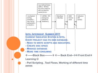
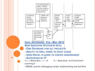
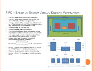
RISHIKESH SHARMA
      (RISHI)
        
User Defined Rules(
                 UDR’s) – Written
                 for Lintra using Lira
                 API’s to check on
                 waiver/errors.

  Lira (System          LINTRA – RTL     Data Base   UNIX      Indicators
 Verilog               linting tool.     ( My SQL)   Environ   (DB
 Compiler) –           (Check for                    ment      Center)
 Has a set of          violations.)
 defined API’s
 in Perl/C++.


INTEL INTERNSHIP SUMMER 2011
CURRENT INDICATOR SYSTEM IN INTEL
EVERY PROJECT HAS ITS OWN DATABASE.
- NEED TO WRITE SCRIPTS AND INDICATORS.
- CREATE DISC SPACE
- MANAGE DATABASE
- MORE TIME CONSUMING
------Black Box--------- --- Back End--Front End
Learning 
- Perl Scripting , Tool Flows, Working of different time
zones
User Defined Rules(
                  UDR’s) – Written
                  for Lintra using Lira
                  APO’s to check on
                  waiver/errors.

  Lira (System           LINTRA – RTL       iBI Data      Power     Indicators
 Verilog                linting tool.       Base (        Pivot     PUMA
 Compiler) –            (Check for          MSSQL)        (Excel    (Performance
 Has a set of           violations.)        - One         Plugin)   Unified
 defined API’s                              centralized             Measurement
 in Perl/C++.                               DB for all              Application)
                                            projects
                                            data

              Gate Keeper(
                                     ibI
             Tool used to
                                     logg
             track Turnins
                                     er
             (Code change
             set)

INTEL INTERNSHIP FEB –MAY 2012
NEW INDICATOR SYSTEM IN INTEL
- ONE DATABASE FOR ALL PROJECTS
- ABILITY TO DRILL DOWN TO ROOT CAUSE
- USES EXCEL PLUGINS TO CREATE DASHBOARDS
- SUPPORTED BY IT
------Black Box---------  --- Back End--Front End
Learning 
- MSSQL queries, Debugging scripts, Implementing new tool flow
DB CENTER VS PUMA
INTEL INTERNSHIP MAY 2012 ONWARDS
-   Create a cloud based solution for current SMB’s
    using Nirvanix Api’s.
-   Virtualize servers for Windows machines.
-   Sync workstations/ Servers using Rsync.
RESEARCH ASSISTANT – SMART GRID CENTER, CSUS
   Smart Grid - A smart grid is a
    digitally enabled electrical grid that
    gathers, distributes, and acts on
    information about the behavior of all
    participants        (suppliers        and
    consumers) in order to improve the
    efficiency,    importance,      reliability,
    economics, and sustainability of
    electricity service that gathers,
    distributes, and acts on information
    about the behavior of all participants
    (suppliers and consumers) in order to
    improve the efficiency, importance,
    reliability,      economics,          and
    sustainability of electricity services.

   OSI Soft – SCADA data analysis
    software.
   FOA 152 – Employee Retraining in
    Power industry sector.
   IEEE Region 6 webmaster.
   CSUS – EEE/CPE webmaster.
PREVIOUS EMPLOYMENT
   Satyam – Bangalore India                           Accenture – Bangalore India
   Solve bug fixes, avoid code redundancy,            Worked in an Enhancement project for Cisco, in
    hard coding of frequently changing values.          the Customer Relationship Management(CRM)
                                                        domain, on the Salesforce.com tool. The project
   Web based POC project, for a Web based
                                                        focused on improving the current application and
    application that offered personalized wealth
                                                        also adding new features and requirements to the
    management on the Web. module related to
                                                        process. The project involves reverse engineering
    credit cards
                                                        and implementing the business logic in the
   Customize the Eclipse tool as per company           Salesforce.com tool.
    specific requirements, which would ease their
    operation.
   Development of a mobile application based on       Responsibility
    concept of Context Map.
                                                       Analysis of Functional and Business requirements.
   Environment: Java, XML, HTML, Java
                                                       Appling changes and writing test cases.
    script, AJAX, XML, Struts, Springs,
    Hibernate, MYSQL, Net Beans, Eclipse 3.2,          Design of requirements provided by the client.
    Windows XP.                                        Carrying out ongoing change requests.
                                                       Environment: Salesforce.com, Apex, Visual Force
                                                        Page, JavaScript, Eclipse Ganymede, Windows
                                                        Vista.
FIFO – BASED ON SYSTEM VERILOG DESIGN / VERIFICATION
   1-bit input flush: clears every location in the FIFO
   1-bit input insert: When asserted, data on data_in is
    stored at the tail of FIFO on posedge of clock
   1-bit input remove: When asserted, data at the head of
    the FIFO is removed from the FIFO and placed on the on
    data_out output port on positive edge of clock
   32-bit input data_in: input data port
   32-bit output data_out: output data port
   1-bit output full: asserted on the positive edge of clock
    when the buffer is full and there is no more room for data
   1-bit output empty: asserted on positive edge of clock
    when the buffer is empty (no data in the buffer)
   Full and empty flags are used by the external
    environment for proper use of the FIFO


   Develop a System Verilog interface that can be used in
    the FIFO (DUT) and the test bench environment.
   Utilize the class concept to fully test the functionality
   Develop a System Verilog program block for testing the
    FIFO.
PCI DESIGN
   Designing Master/Target handshake for a PCI
    device involving a memory write with three data
    phases for an optimized address at a PCI clock
    33MHZ providing test bench and simulation
    results.


   Block diagram (high-level      design),   state
    machine, and program code


   In the verilog design we have made an initiator
    and target device to do 3 optimized write
    phases. The signal values are checked at the
    positive edge of clock and driven on the
    negative edge as required in PCI specs.
PARALLEL PIPELINED MATRIX MULTIPLIER
   A and B are pre-stored in memory. Elements of A, B, and P are 32-bit integers. P should be
    stored in memory. You can have up to four 32-bit wide memory banks.
   Address port for a memory bank is 32-bit..
   Memory bank gets proper control and address signals, it needs 8 cycles to retrieve or write 32
    bits. The address phase takes one cycle.
   Arithmetic unit can only operate on register-type data.
   The results of the ALU cannot directly be written into the memory block.
   The multiplication of two matrices A and B will begin when an input signal called START is
    asserted.
   PMM will assert and output signal called “DONE” when multiplication is done.
   Develop a test bench for validating the data path.
   Synthesize PMM and analyze the synthesized circuit using Synopsis Design Compiler tool.
   VCS - Verilog Simulator – simulate / Code Coverage.
   VCS – Design Complier – Synthesis Tool.
   VCS – Design vision – Interface to communicate with the DC.


                                                                                                        1.ADDRESS_STORE_A
                                                                                                        2. ADDRESS_STORE_B_EVEN ,ADDRESS_STORE_B_ODD
                                                                                                        3. DATA_MATRIX_A    -    A[7:0],A[15:8],A[23:16],A[31:24]
                                                                                                        4. DATA _MATRIX_B   - B_EVEN,B_ODD
                                                                                                        5. DATA_MUL_A       6. DATA_MUL_B         7. MUL_OUTPUT        8. ADD_OUTPUT
                                                                                                        9. EXEC_MEM_P_EVEN        10. EXEC_MEM_P_ODD           11. EXEC_MEM_P_EVEN
                                                                                                        12. EXEC_MEM_P_ODD        13.MEM_WB_P_EVEN             14. MEM_WB_P_ODD
                                                                                                        15. REG_OUTPUT          16.TEMP_REGISTER_EVEN          TEMP_REGISTER_ODD
                                                                                                        17. TEMP_REGISTER_EVEN [31:0]        TEMP_REGISTER_EVEN [63:32]
                                                                                                                         TEMP_REGISTER_ODD[31:0]             TEMP_REGISTER_ODD [63:32]
                                                                                                        18. DATA_MATRIX_P
STANDARD CELL LIBRARY
   Design and layout digital standard cell library in 90nm CMOS using Microwind CAD tool involving basic and complex CMOS
    logic gates without DRC error.
   Technology file called “cmos90n.rul”. Minimize the area used.
   VDD bus on top and a GND bus on the bottom of the cell, with each bus made out of metal 6 which is 5µm wide.
   All cell inputs and outputs other than VDD and GND should come out to the bottom of the cell in metal 3.
   Route connections using metal such that even metals route horizontal and odd metals route vertical.
   Devices as small as possible. Metal routing as close.
One Person Can Make a Difference And Everyone Should Try !!! 

Rishikesh Sharma Portfolio

  • 1.
    RISHIKESH SHARMA (RISHI) 
  • 2.
    User Defined Rules( UDR’s) – Written for Lintra using Lira API’s to check on waiver/errors. Lira (System LINTRA – RTL Data Base UNIX Indicators Verilog linting tool. ( My SQL) Environ (DB Compiler) – (Check for ment Center) Has a set of violations.) defined API’s in Perl/C++. INTEL INTERNSHIP SUMMER 2011 CURRENT INDICATOR SYSTEM IN INTEL EVERY PROJECT HAS ITS OWN DATABASE. - NEED TO WRITE SCRIPTS AND INDICATORS. - CREATE DISC SPACE - MANAGE DATABASE - MORE TIME CONSUMING ------Black Box--------- --- Back End--Front End Learning  - Perl Scripting , Tool Flows, Working of different time zones
  • 3.
    User Defined Rules( UDR’s) – Written for Lintra using Lira APO’s to check on waiver/errors. Lira (System LINTRA – RTL iBI Data Power Indicators Verilog linting tool. Base ( Pivot PUMA Compiler) – (Check for MSSQL) (Excel (Performance Has a set of violations.) - One Plugin) Unified defined API’s centralized Measurement in Perl/C++. DB for all Application) projects data Gate Keeper( ibI Tool used to logg track Turnins er (Code change set) INTEL INTERNSHIP FEB –MAY 2012 NEW INDICATOR SYSTEM IN INTEL - ONE DATABASE FOR ALL PROJECTS - ABILITY TO DRILL DOWN TO ROOT CAUSE - USES EXCEL PLUGINS TO CREATE DASHBOARDS - SUPPORTED BY IT ------Black Box--------- --- Back End--Front End Learning  - MSSQL queries, Debugging scripts, Implementing new tool flow
  • 4.
  • 5.
    INTEL INTERNSHIP MAY2012 ONWARDS - Create a cloud based solution for current SMB’s using Nirvanix Api’s. - Virtualize servers for Windows machines. - Sync workstations/ Servers using Rsync.
  • 6.
    RESEARCH ASSISTANT –SMART GRID CENTER, CSUS  Smart Grid - A smart grid is a digitally enabled electrical grid that gathers, distributes, and acts on information about the behavior of all participants (suppliers and consumers) in order to improve the efficiency, importance, reliability, economics, and sustainability of electricity service that gathers, distributes, and acts on information about the behavior of all participants (suppliers and consumers) in order to improve the efficiency, importance, reliability, economics, and sustainability of electricity services.  OSI Soft – SCADA data analysis software.  FOA 152 – Employee Retraining in Power industry sector.  IEEE Region 6 webmaster.  CSUS – EEE/CPE webmaster.
  • 7.
    PREVIOUS EMPLOYMENT  Satyam – Bangalore India  Accenture – Bangalore India  Solve bug fixes, avoid code redundancy,  Worked in an Enhancement project for Cisco, in hard coding of frequently changing values. the Customer Relationship Management(CRM) domain, on the Salesforce.com tool. The project  Web based POC project, for a Web based focused on improving the current application and application that offered personalized wealth also adding new features and requirements to the management on the Web. module related to process. The project involves reverse engineering credit cards and implementing the business logic in the  Customize the Eclipse tool as per company Salesforce.com tool. specific requirements, which would ease their operation.  Development of a mobile application based on  Responsibility concept of Context Map.  Analysis of Functional and Business requirements.  Environment: Java, XML, HTML, Java  Appling changes and writing test cases. script, AJAX, XML, Struts, Springs, Hibernate, MYSQL, Net Beans, Eclipse 3.2,  Design of requirements provided by the client. Windows XP.  Carrying out ongoing change requests.  Environment: Salesforce.com, Apex, Visual Force Page, JavaScript, Eclipse Ganymede, Windows Vista.
  • 8.
    FIFO – BASEDON SYSTEM VERILOG DESIGN / VERIFICATION  1-bit input flush: clears every location in the FIFO  1-bit input insert: When asserted, data on data_in is stored at the tail of FIFO on posedge of clock  1-bit input remove: When asserted, data at the head of the FIFO is removed from the FIFO and placed on the on data_out output port on positive edge of clock  32-bit input data_in: input data port  32-bit output data_out: output data port  1-bit output full: asserted on the positive edge of clock when the buffer is full and there is no more room for data  1-bit output empty: asserted on positive edge of clock when the buffer is empty (no data in the buffer)  Full and empty flags are used by the external environment for proper use of the FIFO  Develop a System Verilog interface that can be used in the FIFO (DUT) and the test bench environment.  Utilize the class concept to fully test the functionality  Develop a System Verilog program block for testing the FIFO.
  • 9.
    PCI DESIGN  Designing Master/Target handshake for a PCI device involving a memory write with three data phases for an optimized address at a PCI clock 33MHZ providing test bench and simulation results.  Block diagram (high-level design), state machine, and program code  In the verilog design we have made an initiator and target device to do 3 optimized write phases. The signal values are checked at the positive edge of clock and driven on the negative edge as required in PCI specs.
  • 10.
    PARALLEL PIPELINED MATRIXMULTIPLIER  A and B are pre-stored in memory. Elements of A, B, and P are 32-bit integers. P should be stored in memory. You can have up to four 32-bit wide memory banks.  Address port for a memory bank is 32-bit..  Memory bank gets proper control and address signals, it needs 8 cycles to retrieve or write 32 bits. The address phase takes one cycle.  Arithmetic unit can only operate on register-type data.  The results of the ALU cannot directly be written into the memory block.  The multiplication of two matrices A and B will begin when an input signal called START is asserted.  PMM will assert and output signal called “DONE” when multiplication is done.  Develop a test bench for validating the data path.  Synthesize PMM and analyze the synthesized circuit using Synopsis Design Compiler tool.  VCS - Verilog Simulator – simulate / Code Coverage.  VCS – Design Complier – Synthesis Tool.  VCS – Design vision – Interface to communicate with the DC.  1.ADDRESS_STORE_A  2. ADDRESS_STORE_B_EVEN ,ADDRESS_STORE_B_ODD  3. DATA_MATRIX_A - A[7:0],A[15:8],A[23:16],A[31:24]  4. DATA _MATRIX_B - B_EVEN,B_ODD  5. DATA_MUL_A 6. DATA_MUL_B 7. MUL_OUTPUT 8. ADD_OUTPUT  9. EXEC_MEM_P_EVEN 10. EXEC_MEM_P_ODD 11. EXEC_MEM_P_EVEN  12. EXEC_MEM_P_ODD 13.MEM_WB_P_EVEN 14. MEM_WB_P_ODD  15. REG_OUTPUT 16.TEMP_REGISTER_EVEN TEMP_REGISTER_ODD  17. TEMP_REGISTER_EVEN [31:0] TEMP_REGISTER_EVEN [63:32] TEMP_REGISTER_ODD[31:0] TEMP_REGISTER_ODD [63:32]  18. DATA_MATRIX_P
  • 11.
    STANDARD CELL LIBRARY  Design and layout digital standard cell library in 90nm CMOS using Microwind CAD tool involving basic and complex CMOS logic gates without DRC error.  Technology file called “cmos90n.rul”. Minimize the area used.  VDD bus on top and a GND bus on the bottom of the cell, with each bus made out of metal 6 which is 5µm wide.  All cell inputs and outputs other than VDD and GND should come out to the bottom of the cell in metal 3.  Route connections using metal such that even metals route horizontal and odd metals route vertical.  Devices as small as possible. Metal routing as close.
  • 12.
    One Person CanMake a Difference And Everyone Should Try !!! 