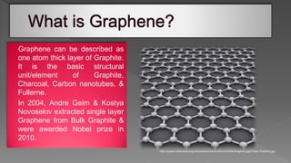
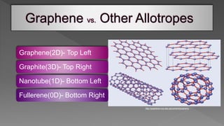
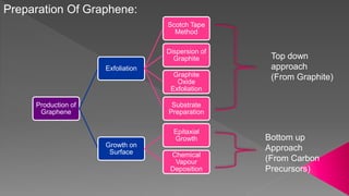
NAME: SUNAMRO
SARKAR
ROLL NUMBER:1455018
6th SEMESTER
DATE OF SUBMISSION:
6th FEBBRUARY
B. Tech SEMINAR (CHE 694)
A SEMINAR REPORT ON:
COMPOUNDS FOR POCKET SIZE DATA STORAGE
DEPARTMENT OF CHEMICAL ENGINEERING
HERITAGE INSTITUTE OF TECHNOLOGY, KOLKATA
 Introduction: Compounds of Pocket-size storage
 What is Graphene
 Properties of Graphene
 Preparation of Graphene
 Overview: Methods of preparation of Graphene
 Mechanism of Data Storage
 Summary & Conclusion
 Imagine stashing your mission critical enterprise data in single molecules.
IT providers across the world are taking notice of a new and promising
technology called molecular memory. It could mean that data center
facilities could be storing at least 1000TB of data within a square inch of
space, maximizing critical real estate within their facilities while saving
money on energy usage.
 A research has been carried out by scientists at the Indian Institute of
Science Education and Research (IISER) & MIT lab for invention of a
supermolecule which can materialize the idea of nanoscale storage.
 An international team of scientists, including some from India, has now
created a magnetic supramolecule — by chemically binding two molecules
— to make a device that can transfer and store information in a single
molecular magnetic layer.
Organo-metallic compound containing Zinc atoms chemically linked to flat sheets of
Carbon called Graphene Fragments. The compound is sandwiched between layer
of Cobalt(by growing the crystals of the supramolecule on Cobalt surface) and that
of copper and is found that this layered system could be used to store and read
digital information at about -23°C.
The fundamental material used is a
nano-sized particle called Graphene
Graphene can be described as
one atom thick layer of Graphite.
It is the basic structural
unit/element of Graphite,
Charcoal, Carbon nanotubes, &
Fullerne.
In 2004, Andre Geim & Kostya
Novoselov extracted single layer
Graphene from Bulk Graphite &
were awarded Nobel prize in
2010.
http://upload.wikimedia.org/wikipedia/commons/thumb/9/9e/Graphen.jpg/750px-Graphen.jpg
Graphene(2D)- Top Left
Graphite(3D)- Top Right
Nanotube(1D)- Bottom Left
Fullerene(0D)- Bottom Right
http://graphene.nus.edu.sg/content/graphene
 A single sheet of graphite is called graphene
 It is sp2 hybridized( covalently bonded) & it is bound to its 3 neighbors.
 The bonding between the graphene sheets in graphite is of van der Walls
type. Bond length is .142 nm long = very strong bond
 Strongest & thinnest material discovered till date and is artificially obtained
from Graphite, an allotrope of Carbon.
 Graphene burns at a very low temperature (e.g.,350°C)
 Graphene is the most reactive form of Carbon as each single atom is in
exposure for chemical reaction from 2 sides (due to the 2D structure).
Physical & Chemical Properties of Graphene
 These carbon atoms are bound
within the plane by strong
bonds into a Honeycomb array
consisting of six-membered
rings.
 Graphene is commonly
modified with Oxygen- and
Nitrogen- containing functional
groups.
Physical & Chemical Properties of Graphene
Contd.
Production of
Graphene
Exfoliation
Scotch Tape
Method
Dispersion of
Graphite
Graphite
Oxide
Exfoliation
Substrate
Preparation
Growth on
Surface
Epitaxial
Growth
Chemical
Vapour
Deposition
Top down
approach
(From Graphite)
Bottom up
Approach
(From Carbon
Precursors)
Preparation Of Graphene:
 Scotch & Tape method:
 In this micromechanical exfoliation method, graphene is
detached from a graphite crystal using adhesive tape.
After peeling it off the graphite, multiple-layer graphene
remains on the tape.
 By repeated peeling the multiple-layer graphene is
cleaved into various flakes of few-layer graphene.
 Afterwards the tape is attached to the substrate and the
glue solved, e.g. by acetone, in order to detach the tape.
 Finally one last peeling with an unused tape is
performed.
N.B.-Amongst these methods, Scotch Tape method, Graphite Oxide Exfoliation,
Epitaxial Growth and Chemical Vapour Deposition is widely used for Graphene
extraction.
SOLUTION OF GRAPHENE IN LIQUID
PHASE. THE FLASKS CONTAIN SOLUTIONS
AFTER CENTRIFUGATION AT DIFFERENT
FREQUENCIES
 Graphite Oxide Exfoliation:
 The principle of liquid-phase exfoliation can
also be used to exfoliate graphite oxide. Due
to several functional groups like epoxide or
hydroxyl, graphene oxide is hydrophilic and
can be solved in water by sonication or
stirring.
 Thereby the layers become negatively
charged and thus a recombination is
inhibited by the electrical repulsion.
 After centrifugation the graphene oxide has
to be reduced to regular graphene by
thermal or chemical methods. It is hardly
possible to dispose of all the oxygen. In fact,
an atomic C/O ratio of about 10 still remains.
Scheme of the exfoliation of graphite oxide. The graphite
gets oxidized and solved in water. Afterwards it gets
reduced to graphene.
 Epitaxial Growth(on surface):
Graphene can be prepared by simply heating and cooling down an
SiC crystal. Generally speaking single- or bi-layer graphene forms
on the Si face of the crystal, whereas few-layer graphene grows on
the C face. The results are highly dependent on the parameters
used, like temperature, heating rate, or pressure. In fact, if
temperatures and pressure are too high the growth of nanotubes
instead of graphene can occur. The Ni(111) surface has a lattice
structure very similar to the one of graphene, with a mismatch of the
lattice constant at about 1.3% . Thus by use of the nickel diffusion
method a thin Ni layer is evaporated onto a SiC crystal. Upon
heating the carbon diffuses through the Ni layer and forms a
graphene or graphite layer on the surface, depending on the heating
rate. The thus produced graphene is easier to detach from the
surface than the graphene produced by the growth on a simple SiC
crystal without Ni. The growth of graphene starts at several
locations on the crystal simultaneously and these graphene islands
grow together.
SEM image of graphene on
copper foil. At several
locations on the surface
graphene islands form and
grow together.
 Chemical Vapour Deposition:
Chemical vapour deposition is a well known
process in which a substrate is exposed to
gaseous compounds. These compounds
decompose on the surface in order to grow a thin
film, whereas the by-products evaporate.
Graphene can be grown by exposing of a Ni film
to a gas mixture of H2, CH4 and Ar at about
1000°C. The methane decomposes on the
surface, so that the hydrogen evaporates. The
carbon diffuses into the Ni. After cooling down in
an Ar atmosphere, a graphene layer grows on the
surface, a process similar to the Ni diffusion
method. Hence, the average number of layers
depends on the Ni thickness and can be
controlled in this way. The shape of the graphene
can also be controlled by patterning of the Ni layer
In summary, the exfoliation methods have the
advantage of providing graphene of very high
quality and purity, and, due to the low
complexity, they are perfect for laboratory
research. The sizes of the obtained flakes,
however, as well as the controllability are too
poor for industrial production. On the other
hand, the growth of grapheme on surfaces
allows a more or less unlimited size of the
graphene layers and a high controllability, which
makes these methods applicable for industrial
production. The purity, however, is not very high,
which makes these methods unsuitable for
laboratory research of graphene. Since CVD is
an already used method in industry, the epitaxial
growth of graphene is probably a dead end
technique.
Graphene fragments are found to have a storage capacity of
around 1000Terabytes/sq. inch at a temperature of -23°C. The
mechanism behind such a humongous storage capacity is
molecular spintronics. It is aimed at harnessing a property of
electron called spin. An electron may have an anticlockwise or
clockwise spin in molecules generally denoted by +1/2 or -1/2
respectively while writing the configuration of an electron. By
manipulating the magnetic conductivity of the molecules,
researchers were able to replicate binary ones and zeros in
accordance with the state of the molecules’ magnetism. This
creates molecular memory, which grants us the ability to store even
more data in a small amount of space. Electron spin in molecules
are used as the 0 or 1 binary states for digital data. For total
understanding of the mechanism a brief insight into spintronics is
required.
Conventional electronic devices rely on the transport of electrical charge carriers
electrons in a semiconductor such as silicon. Now, however, physicists are trying to
exploit the 'spin' of the electron rather than its charge to create a remarkable new
generation of 'spintronic' devices which will be smaller, more versatile and more robust.
All spintronic devices act according to the simple scheme:
 (1) information is stored (written) into spins as a particular spin orientation (up or down),
 (2) the spins, being attached to mobile electrons, carry the information along a wire, and
 (3) the information is read at a terminal. Spin orientation of conduction electrons survives
for a relatively long time (nanoseconds, compared to tens of femto-seconds during which
electron momentum decays), which makes spintronic devices particularly attractive for
memory storage and magnetic sensors applications, and, potentially for quantum
computing where electron spin would represent a bit (called qubit) of information.
The concept behind quantum computing is simple. Use quantum
mechanical systems with the full use of their quantum mechanical
properties to do computations. Why is this useful? As was shown
over the years, quantum mechanical dynamics can be used to
compute the answers to certain problems much faster than any
classical system or computer can. For instance numbers can be
factored in polynomial time by quantum computers, compared to
the exponential time of classical ones. This has brought about a
fundamental revolution in the field of complexity theory and
cryptography, among others. This Supramolecule has potential to
serve as the fundamental blocks for Quantum computers thus
materializing the idea of Quantum computing. With this idea we
conclude our discussion here.
Acknowledgement:
I’m sincerely indebted to the faculty members of the Chemical Engineering department of
Heritage Institute of Technology, Kolkata for giving me the chance to produce this
presentation. Since this topic is research oriented, numerous papers, patents and journals
have been referred to for complete detailing of the topic. Some of them include:
 “PREPARATION OF GRAPHENE: Physics of Nanoscale Carbon” by Nils Krane,
 News Article: “Hope for molecule memory- Bengal-made compound for pocket-size
storage”
http://www.telegraphindia.com/1130124/jsp/nation/story_16479071.jsp#.UQDogR04vZI
 E-Journal Article: “Molecular Memory Makes Waves in a Lab at MIT”
 http://californiahosting.net/molecular-memory-makes-waves-in-a-lab-at-mit/
 “A Gentle Introduction to Quantum Computing” by Abdullah Khalid
I’m also greatly indebted to slideshare for providing me the guidance on how to make
presentations and also with sufficient material for the topic of presentation.
Thank You for your attention

Project on pocket size data storage

  • 1.
    NAME: SUNAMRO SARKAR ROLL NUMBER:1455018 6thSEMESTER DATE OF SUBMISSION: 6th FEBBRUARY B. Tech SEMINAR (CHE 694) A SEMINAR REPORT ON: COMPOUNDS FOR POCKET SIZE DATA STORAGE DEPARTMENT OF CHEMICAL ENGINEERING HERITAGE INSTITUTE OF TECHNOLOGY, KOLKATA
  • 2.
     Introduction: Compoundsof Pocket-size storage  What is Graphene  Properties of Graphene  Preparation of Graphene  Overview: Methods of preparation of Graphene  Mechanism of Data Storage  Summary & Conclusion
  • 3.
     Imagine stashingyour mission critical enterprise data in single molecules. IT providers across the world are taking notice of a new and promising technology called molecular memory. It could mean that data center facilities could be storing at least 1000TB of data within a square inch of space, maximizing critical real estate within their facilities while saving money on energy usage.  A research has been carried out by scientists at the Indian Institute of Science Education and Research (IISER) & MIT lab for invention of a supermolecule which can materialize the idea of nanoscale storage.  An international team of scientists, including some from India, has now created a magnetic supramolecule — by chemically binding two molecules — to make a device that can transfer and store information in a single molecular magnetic layer.
  • 4.
    Organo-metallic compound containingZinc atoms chemically linked to flat sheets of Carbon called Graphene Fragments. The compound is sandwiched between layer of Cobalt(by growing the crystals of the supramolecule on Cobalt surface) and that of copper and is found that this layered system could be used to store and read digital information at about -23°C. The fundamental material used is a nano-sized particle called Graphene
  • 5.
    Graphene can bedescribed as one atom thick layer of Graphite. It is the basic structural unit/element of Graphite, Charcoal, Carbon nanotubes, & Fullerne. In 2004, Andre Geim & Kostya Novoselov extracted single layer Graphene from Bulk Graphite & were awarded Nobel prize in 2010. http://upload.wikimedia.org/wikipedia/commons/thumb/9/9e/Graphen.jpg/750px-Graphen.jpg
  • 6.
    Graphene(2D)- Top Left Graphite(3D)-Top Right Nanotube(1D)- Bottom Left Fullerene(0D)- Bottom Right http://graphene.nus.edu.sg/content/graphene
  • 7.
     A singlesheet of graphite is called graphene  It is sp2 hybridized( covalently bonded) & it is bound to its 3 neighbors.  The bonding between the graphene sheets in graphite is of van der Walls type. Bond length is .142 nm long = very strong bond  Strongest & thinnest material discovered till date and is artificially obtained from Graphite, an allotrope of Carbon.  Graphene burns at a very low temperature (e.g.,350°C)  Graphene is the most reactive form of Carbon as each single atom is in exposure for chemical reaction from 2 sides (due to the 2D structure). Physical & Chemical Properties of Graphene
  • 8.
     These carbonatoms are bound within the plane by strong bonds into a Honeycomb array consisting of six-membered rings.  Graphene is commonly modified with Oxygen- and Nitrogen- containing functional groups. Physical & Chemical Properties of Graphene Contd.
  • 9.
    Production of Graphene Exfoliation Scotch Tape Method Dispersionof Graphite Graphite Oxide Exfoliation Substrate Preparation Growth on Surface Epitaxial Growth Chemical Vapour Deposition Top down approach (From Graphite) Bottom up Approach (From Carbon Precursors) Preparation Of Graphene:
  • 10.
     Scotch &Tape method:  In this micromechanical exfoliation method, graphene is detached from a graphite crystal using adhesive tape. After peeling it off the graphite, multiple-layer graphene remains on the tape.  By repeated peeling the multiple-layer graphene is cleaved into various flakes of few-layer graphene.  Afterwards the tape is attached to the substrate and the glue solved, e.g. by acetone, in order to detach the tape.  Finally one last peeling with an unused tape is performed. N.B.-Amongst these methods, Scotch Tape method, Graphite Oxide Exfoliation, Epitaxial Growth and Chemical Vapour Deposition is widely used for Graphene extraction. SOLUTION OF GRAPHENE IN LIQUID PHASE. THE FLASKS CONTAIN SOLUTIONS AFTER CENTRIFUGATION AT DIFFERENT FREQUENCIES
  • 11.
     Graphite OxideExfoliation:  The principle of liquid-phase exfoliation can also be used to exfoliate graphite oxide. Due to several functional groups like epoxide or hydroxyl, graphene oxide is hydrophilic and can be solved in water by sonication or stirring.  Thereby the layers become negatively charged and thus a recombination is inhibited by the electrical repulsion.  After centrifugation the graphene oxide has to be reduced to regular graphene by thermal or chemical methods. It is hardly possible to dispose of all the oxygen. In fact, an atomic C/O ratio of about 10 still remains. Scheme of the exfoliation of graphite oxide. The graphite gets oxidized and solved in water. Afterwards it gets reduced to graphene.
  • 12.
     Epitaxial Growth(onsurface): Graphene can be prepared by simply heating and cooling down an SiC crystal. Generally speaking single- or bi-layer graphene forms on the Si face of the crystal, whereas few-layer graphene grows on the C face. The results are highly dependent on the parameters used, like temperature, heating rate, or pressure. In fact, if temperatures and pressure are too high the growth of nanotubes instead of graphene can occur. The Ni(111) surface has a lattice structure very similar to the one of graphene, with a mismatch of the lattice constant at about 1.3% . Thus by use of the nickel diffusion method a thin Ni layer is evaporated onto a SiC crystal. Upon heating the carbon diffuses through the Ni layer and forms a graphene or graphite layer on the surface, depending on the heating rate. The thus produced graphene is easier to detach from the surface than the graphene produced by the growth on a simple SiC crystal without Ni. The growth of graphene starts at several locations on the crystal simultaneously and these graphene islands grow together. SEM image of graphene on copper foil. At several locations on the surface graphene islands form and grow together.
  • 13.
     Chemical VapourDeposition: Chemical vapour deposition is a well known process in which a substrate is exposed to gaseous compounds. These compounds decompose on the surface in order to grow a thin film, whereas the by-products evaporate. Graphene can be grown by exposing of a Ni film to a gas mixture of H2, CH4 and Ar at about 1000°C. The methane decomposes on the surface, so that the hydrogen evaporates. The carbon diffuses into the Ni. After cooling down in an Ar atmosphere, a graphene layer grows on the surface, a process similar to the Ni diffusion method. Hence, the average number of layers depends on the Ni thickness and can be controlled in this way. The shape of the graphene can also be controlled by patterning of the Ni layer
  • 14.
    In summary, theexfoliation methods have the advantage of providing graphene of very high quality and purity, and, due to the low complexity, they are perfect for laboratory research. The sizes of the obtained flakes, however, as well as the controllability are too poor for industrial production. On the other hand, the growth of grapheme on surfaces allows a more or less unlimited size of the graphene layers and a high controllability, which makes these methods applicable for industrial production. The purity, however, is not very high, which makes these methods unsuitable for laboratory research of graphene. Since CVD is an already used method in industry, the epitaxial growth of graphene is probably a dead end technique.
  • 15.
    Graphene fragments arefound to have a storage capacity of around 1000Terabytes/sq. inch at a temperature of -23°C. The mechanism behind such a humongous storage capacity is molecular spintronics. It is aimed at harnessing a property of electron called spin. An electron may have an anticlockwise or clockwise spin in molecules generally denoted by +1/2 or -1/2 respectively while writing the configuration of an electron. By manipulating the magnetic conductivity of the molecules, researchers were able to replicate binary ones and zeros in accordance with the state of the molecules’ magnetism. This creates molecular memory, which grants us the ability to store even more data in a small amount of space. Electron spin in molecules are used as the 0 or 1 binary states for digital data. For total understanding of the mechanism a brief insight into spintronics is required.
  • 16.
    Conventional electronic devicesrely on the transport of electrical charge carriers electrons in a semiconductor such as silicon. Now, however, physicists are trying to exploit the 'spin' of the electron rather than its charge to create a remarkable new generation of 'spintronic' devices which will be smaller, more versatile and more robust. All spintronic devices act according to the simple scheme:  (1) information is stored (written) into spins as a particular spin orientation (up or down),  (2) the spins, being attached to mobile electrons, carry the information along a wire, and  (3) the information is read at a terminal. Spin orientation of conduction electrons survives for a relatively long time (nanoseconds, compared to tens of femto-seconds during which electron momentum decays), which makes spintronic devices particularly attractive for memory storage and magnetic sensors applications, and, potentially for quantum computing where electron spin would represent a bit (called qubit) of information.
  • 17.
    The concept behindquantum computing is simple. Use quantum mechanical systems with the full use of their quantum mechanical properties to do computations. Why is this useful? As was shown over the years, quantum mechanical dynamics can be used to compute the answers to certain problems much faster than any classical system or computer can. For instance numbers can be factored in polynomial time by quantum computers, compared to the exponential time of classical ones. This has brought about a fundamental revolution in the field of complexity theory and cryptography, among others. This Supramolecule has potential to serve as the fundamental blocks for Quantum computers thus materializing the idea of Quantum computing. With this idea we conclude our discussion here.
  • 18.
    Acknowledgement: I’m sincerely indebtedto the faculty members of the Chemical Engineering department of Heritage Institute of Technology, Kolkata for giving me the chance to produce this presentation. Since this topic is research oriented, numerous papers, patents and journals have been referred to for complete detailing of the topic. Some of them include:  “PREPARATION OF GRAPHENE: Physics of Nanoscale Carbon” by Nils Krane,  News Article: “Hope for molecule memory- Bengal-made compound for pocket-size storage” http://www.telegraphindia.com/1130124/jsp/nation/story_16479071.jsp#.UQDogR04vZI  E-Journal Article: “Molecular Memory Makes Waves in a Lab at MIT”  http://californiahosting.net/molecular-memory-makes-waves-in-a-lab-at-mit/  “A Gentle Introduction to Quantum Computing” by Abdullah Khalid I’m also greatly indebted to slideshare for providing me the guidance on how to make presentations and also with sufficient material for the topic of presentation.
  • 19.
    Thank You foryour attention